Abstract
SUDARSANAM, YASASWINI. Implementation of Double Precision Floating Point Arithmetic. (Under the guidance of Dr.Paul Franzon.)
Floating Point Arithmetic is extensively used in the field of medical imaging, biometrics, motion capture and audio applications, including broadcast, conferencing, musical instruments and professional audio. Many of these applications need to solve sparse linear systems that use fair amounts of matrix multiplication.
The objective of this thesis is to implement double precision floating point cores for addition and multiplication .These cores are targeted for Field Programmable Gate Arrays because FPGAs give the designer good control over the number of I/O pins and utilization of on chip memory. FPGAs are also comparable to floating point processors in their power consumption.
Implementation of a Double Precision Floating Point Arithmetic
by
Yasaswini Sudarsanam
A thesis submitted to the graduate faculty of North Carolina State University
in partial fulfillment of the requirements for the Degree of
Master of Science
Computer Engineering
Raleigh, North Carolina
2006
Approved by:
__________________________ __________________________
Dr.Xun Liu Dr.W.Rhett Davis
____________________________________
Dr.Paul Franzon
Biography
Acknowledgement
Thanks to the almighty for whatever little I have achieved till today. I would like to thank my mother who is my first school. All my learning in measures small or large, I owe it to her strong will, determination and even and carefully measured amounts of care and control. I owe it to my father to take success and failure in stride. His conversations though casual were always filled with deep inner thought and meaning. They have guided me even as I stayed away from home during my Masters. This Masters would have remained just a dream if not for my parents’ foresighted thinking and patience with me during insane moments.
My sincere thanks to my advisor Dr.Paul Franzon for his support during the course of my thesis. The independence in both thought and execution that he has allowed has gone a long way in helping me understand the nuances of research per se. I am equally thankful to Dr.Rhett Davis and Dr.Xun Liu for their consent to be on the committee and for their valuable feedback on the thesis document. I would like to acknowledge Dr.Trussell’s valuable suggestions and interest regarding my plan of work towards my Masters.
I would like to thank Manav and Ambrish for their help many a time during the course of the thesis. Thanks to Steve Lipa for help with regard to the licenses. My thanks are due in large proportions to John English of Aware Inc., Boston, MA for his prompt replies and help at various points during the course of my thesis. His suggestions from his vast industry experience have gone a long way in moulding my thought and preparation before design.
Special thanks to Sreeram, Raju, Suresh, Savitha, Subathra and Arundhati for making my stay at NC State eventful. I sincerely thank Srivats for the wonderful support, good cheer and encouragement he has offered during my graduate study. It has been absolutely wonderful staying with you guys.
Contents
List of Figures ……….………...vii
List of Tables ...………viii
1 Introduction ………...1
1.1 Importance ………1
1.2 Idea of Floats ……….………1
1.3 Motivation ………..………1
1.4 Outline of Thesis ………2
2 Double Precision ………3
2.1 Introduction ………3
2.2 Scientific Notation ………3
2.3 Floating Point Unit ………4
2.3.1 Real Number System ………...4
2.3.2 Normalization ………6
2.3.3 Biased exponent ………7
2.3.4 Signed Exponent, Signed Infinity and NaN ………7
2.4 Flipside of Floating Point ………9
3 Design and Implementation ……….11
3.1 IEEE 754 format for Double Precision ………11
3.2 A Simple Example ………...12
3.3 Description of Floating Point ………12
3.3.1 The Floating Point multiplier ………13
3.3.1.1. Module denormalizer ……….13
3.3.1.2 Module multiplier ………14
3.3.1.3 Module normalizer and rounding ………18
3.3.2 Floating point adder ………18
3.3.2.1 Module denormalizer ………19
3.3.2.2 Module shifter ………...19
3.3.2.4 Module rounding ………21
3.3.2.5 Module sign ………23
3.4 The Sparse Matrix ………23
3.4.1 Row Compressed Format ……….24
3.4.2 Basic Architecture ……….24
3.4.2.1 Module descriptions ………25
4 Verification ……….29
5 Results ………31
5.1 Simulation ……….31
5.2 Synthesis ………32
6 Conclusions and future work ………43
References ……….44
LIST OF
FIGURES
Fig 3.1 Double precision representation ………11
Fig 3.2 Expression to calculate value from IEEE 754 format ………12
Fig 3.3 High level view of Floating point multiplier core ………14
Fig 3.4 Comparator v8.0 ………15
Fig 3.5 Fixed Point mantissa multiplier ………16
Fig 3.6 Floating point adder/subtractor core v7.0 ………17
Fig 3.7 Top view – Denormalizer ………20
Fig 3.8 Bit sequence after right shift ……….21
Fig 3.9 Priority encoding in rounding module ………22
Fig 3.10 A sample sparse matrix ………24
Fig 3.11 A simple matrix multiplication architecture ……….25
Fig 3.12 Pipelined divider v3.0 ………26
Fig 5.1 Simulation results from adder ……….32
Fig 5.2 Simulation results from the multiplier ……….33
Fig 5.3 Variation of power with pipelines in 64 bit adder ………39
Fig 5.4 Variation of freq/area vs. pipelines in 64 bit adder ………40
Fig 5.5 Snapshot of the 64 bit multiplier after place and route ………41
LIST OF
TABLES
Table 2.1 Example of floating point format ………5
Table 2.2 Representation of a number in sign, mantissa & exponent format ……….5
Table 2.3 Gradual underflow ………7
Table 2.4 Signed Infinities ………8
Table 3.1 Sign, Exponent & Mantissa limits in IEEE 754 format ………12
Table 3.2 Allowable bit widths & depth of pipelines in comparator v8.0 ……….……16
Table 3.3 Rules for rounding ………18
Table 3.4 Determination of sign ………23
Table 5.1 Variation of freq/area with pipelining for 64 bit multiplier ………34
Table 5.2 Comparison of results from the synthesis of multiplier ………36
Table 5.3 Power vs. pipelining for 64 bit multiplier ………36
Table 5.4 Synthesis results from 64 bit adder ………37
Table 5.5 Comparison of minimum, maximum and optimal metric for adder …………37
Table 5.6 Table of metric comparisons for 64 bit adder ………38
Chapter 1
Introduction
1.1 Importance
Floating point arithmetic is no longer as esoteric as before because of its increasing importance in computer systems. Manipulating floating points efficiently is an utmost necessity as can be seen from the fact that every language supports a floating point data type. Every computer has a floating point processor or a dedicated accelerator that fulfills the requirements of precision using detailed floating point arithmetic. The main applications of floating points today are in the field of medical imaging, biometrics, motion capture and audio applications, including broadcast, conferencing, musical instruments and professional audio. Their importance can be hardly over emphasized because the performances of computers that handle such applications are measured in terms of the number of floating point operations they perform per second or FLOPS /sec.
1.2 Idea of “Floats”
Decimal numbers are also called Floating Points because a single number can be represented with one or more significant digits depending on the position of the decimal point. Since the point floats between the mass of digits that represent the number such numbers are termed Floating Point Numbers. Floating point formats and number representations are discussed in detail in subsequent chapters.
1.3 Motivation
arithmetic intensity of computations portraying a historic growth rate of 71% per year, double and quadruple precision floating points have come to stay.
The double precision cores for addition and multiplication discussed in this thesis are targeted for Virtex II Pro FPGA. In general, the most significant and inherent advantage of FPGAs over a Von Neumann platform is their iteration level parallelism that is one to two orders of magnitude than is available with CPUs. Current FPGAs provide a large amount of on chip memory and abundant I/O pins. Thus they are able to offer a large amount of on-chip and off-chip memory bandwidth to I/O bound applications. This eliminates latencies due to cache misses.
The clock frequency of traditional processors is about 20 times that of typical FPGA implementations. However the efficiency advantage because of the overlap of control and data flow and elimination of some instruction on the FPGA outweigh this advantage resulting in a speedup that is one to two orders in magnitude.[1]. For example, a stand alone hardware implementation of the GIMPS algorithm is reported to be capable of 12-million digit numbers in fewer than 34 milliseconds which is identified as a 1.76 times performance improvement compared to a fast Pentium. [2].
Implementation of 64 bit multiplier and adder cores is an important part of this thesis. In order to demonstrate one of the applications of these cores, basic level matrix
multiplication architecture is established. The performance of the cores are evaluated individually and compared with results obtained from different sources. Power consumption for different levels of pipelining are also tabulated and analyzed .The
implementation uses Xilinx ISE 8.2i Verilog with ModelSim 6.1i for simulation, XST for synthesis.
1.4 Outline of Thesis
Chapter 2
Double Precision
2.1 Introduction
When infinitely large real numbers are to be stored using a finite number of bits, some form of approximation in representation is needed. Most processors use a single word to represent a number and hence these representations of floating point values are called single precision. Double precision floating points are named relative to the single precision representation in the sense that they have twice as much precision and hence twice as many bits as a regular floating point number. This also means that when represented in scientific notation double precision floating points carry more digits to the right of the decimal point. If a single precision number requires 32 bits, a double requires 64 bits. These extra bits also allow an increase in the range of values that can be represented. However this increase is dependent on the program format for a floating point representation. Double precision provides a greater range, approximately 10** (-308) to 10** 308 and about 15 decimal digits of precision compared to a single precision whose approximate range is 10** (-38) to 10**38, with about 7 decimal digits of precision.
2.2 Scientific Notation
Before the discussion of available floating point formats, it is worthy to understand scientific notations. A scientific notation is just another way to represent very large or very small numbers in a compact form such that they can be easily used for computations.
can be simply represented as 3*1010 cm per sec. This involves storage of only the mantissa namely 3 and the exponent which is 10 here.
Scientific notations are mandatory in computation because they greatly simplify multiplications or divisions into mere addition or subtraction of related exponents or powers of 10 used in their representation. For example, multiplication of 132,000,000 by 0.0000231 involves conversion to scientific notation first. This means multiplying 1.32 * 108 by 2.31 * 10-5. This reduces to (1.32 * 2.31) * 10 (8 -5 =3). Extending the idea of such a representation to the binary system helps understand the IEEE 754 format for 64 bit numbers.
2.3 Floating Point Unit
This section describes the real number system and the floating point unit. It introduces terms like normalized numbers, denormalized numbers, biased exponents, and signed zeros and NaNs. It further expands to the understanding of Floating point formats, specific merits and demerits as well as their individualistic applications. It also explains the choice of IEEE floating point format.
2.3.1 Real Number System
The real number system consists of the entire spectrum of numbers between – infinity and + infinity. The limitation on size and number of registers in a computer leaves us with the ability to use only a subset of the real number continuum in calculations. This is just an approximate representation of the real number system, the range and precision being determined by the format of the floating point unit.
A Floating Point Unit or an FPU generally contains 3 parts:
1. Sign
Sign is a 1 bit number that indicates whether the number is positive or negative. The significand has two parts , a one bit binary integer and a binary fraction The one bit binary integer is also known as the J-bit and is an implied value. The significand is also termed the mantissa.
Mantissa and Significand
Mantissa was originally the fractional part of the logarithm while the characteristic was the integer part. Since logarithmic tables were replaced by computers eventually, though not in the pure form, mantissa and significand are used interchangeably in common parlance. A logarithmic table is a table of mantissas. Therefore, mantissa is just the logarithm of the significand.
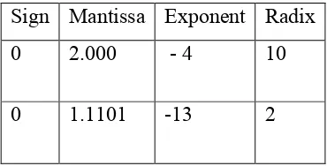
The exponent indicates the positive or the negative power to which the radix should be raised in the computation of the value of a number that is being represented. For example, if 0.0002 is represented in decimal and binary in the sign, mantissa and exponent format it would be as shown in the table 2.1.
Table 2.1 Example of floating point format
Sign Mantissa Exponent Radix
0 2.000 - 4 10
0 1.1101 -13 2
Table 2.2 .Representations of a number in the sign, mantissa and exponent format
Sign Mantissa Exponent
0 1.0 0
0 0.1 1
Each floating point number has multiple representations because of the inherent nature of the decimal point to float between each of the individual digits. Therefore a simple number say 1 can take different forms in a given radix. Table 2.2 lists a few of the possible sign, magnitude and exponent format of the number ‘1’.
Every number can be represented by applying the following on the sign, mantissa and the exponent.
Value = (-1) sign * Mantissa * radix exponent
However, each number has only one normalized form and hence the importance of normalization in floating point arithmetic.
2.3.2 Normalization
A floating point number is said to be normalized if it obeys the following rule:
1/r <= M < 1,
where r is the radix of the system of representation and M is the mantissa.
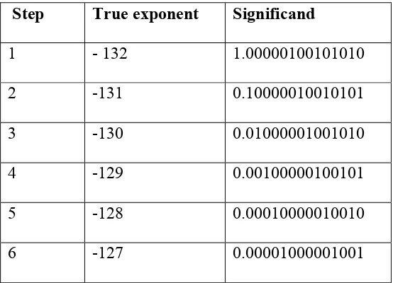
Table 2.3. Gradual Underflow
Step True exponent Significand
1 - 132 1.00000100101010
2 -131 0.10000010010101
3 -130 0.01000001001010
4 -129 0.00100000100101
5 -128 0.00010000010010
6 -127 0.00001000001001
In Table 2.3, step 1 shows the actual result of an operation. The process of gradual underflow does one right shift in each successive step until the exponent reaches a value that which added to the constant bias yields zero. The table depicts the process of denormalization for a 32 bit floating point number where in the bias is +12710.
2.3.3 Biased Exponent
A biased exponent is one that is obtained by adding a constant value to the original exponent. It is done so as to accommodate negative exponents in the chosen format. The choice of the bias is made depending on the number of bits available for representing exponents in the floating point format used. Always when a bias is chosen, one should be able to reciprocate the smallest normalized number without having to deal with problems of overflow. A 32 bit number has a bias of +127 while a 64 bit number has a bias of +1023. If the number of bits allowed for exponent representation is n, the bias is 2n – 1 - 1.
2.3.4 Signed Zero, Signed Infinity and NaN
Zero is known as the neutral number with regard to sign. Both encodings of zero, a plus or a minus are equal in value .The sign of zero depends on two factors:
2. Rounding mode
Signed zeros are a useful aid in implementing interval arithmetic. During approximations of a real number by a floating point number system, one can adopt the usage of one floating point number or two. In case of the latter, there is an additional expense but if these two numbers are on either side of the real number under consideration, then it is possible to say that the number belongs to a set of real numbers bounded by the two floating point numbers. Therefore, any operation executes on this interval. Outward rounding confirms that the result of the computation is always within the resulting interval. Sign of a zero can mean one of the following two:
1. The direction on the number line from which underflow occurred. 2. The sign of infinity reciprocated.
Signed infinity represents the maximum positive and minimum negative number that can be accommodated in a given format. Signed infinity is represented by a zero in the mantissa and the maximum exponent that the representation allows.
For example, in IEEE 754 format for single precision, +∞ and -∞ are represented as
in Table 2.4.
Table2.4 Signed Infinities
NaN or “Not A Number” refers to those values whose mantissas are nonzero and exponent exceeds the maximum allowable value for a format. NaNs are classified as Quiet NaNs and Signaling NaNs. Quiet NaNs are passed by processors without exceptions when encountered but signaling NaNs might raise exceptions.
Number Sign Exponent Mantissa
+∞ 0 255 0
2.4 Flipside of Floating Points
Much as floating points provide greater range of precision as compared to integers, results of floating point calculations can be strange and seemingly inexact. Floating point representation on digital systems is base 2 but the external representation is always base 10. This explains the misconception that a recurring decimal like 1/3 may not be exactly represented but 0.1 or 0.01 can be. However the representation of 0.01 may also be 0.009999 when converted from the binary equivalent that gets stored.
Another noticeable fact is that the exponent and density of numbers represented are inversely proportional. Since there is always approximation to the nearest value in case of non representable values, it is found mathematically that there can be as many as 8,338,607 single precision numbers between 1 and 2 and only 8191 numbers between 1023 and 1024. Rounding can lead to different values even with mathematically equivalent expressions. An example is the use of a divide and multiply operation with a number and its reciprocal respectively.
When such floats are converted to integer, inaccuracies can be well detected. A number written in decimal as xx.ff can be converted to integer by means of a multiply by 100 operation. The result surprisingly is not xxff but xxff – 1. This is because there is no rounding, only truncation during its assignment from float to Integer.
Conversions from single precision to double can be a little dangerous if they need to be eventually converted to integers because the computer inherently pads zeros in the binary representation to extend single to double. The decimal equivalent of the new value can display way more than the actual value.
Chapter 3
Design and Implementation
This chapter deals with the design and implementation of the floating point cores for the sparse matrix multiplier. It explains the hierarchy of modules, the function of each module, implementation details and issues during their simulation and synthesis. The following sections are dedicated to the discussion of the implementation details of the floating point multiplier and adder for double precision. The algorithms for implementation of the adder and multiplier have been adapted for use in the problem from [3]. The idea of the design is drawn from [4].
3.1 IEEE 754 Format for Double Precision
Before delving into design, it is advantageous to understand the IEEE 754 format for double precision that forms the basis of these computations. [5]
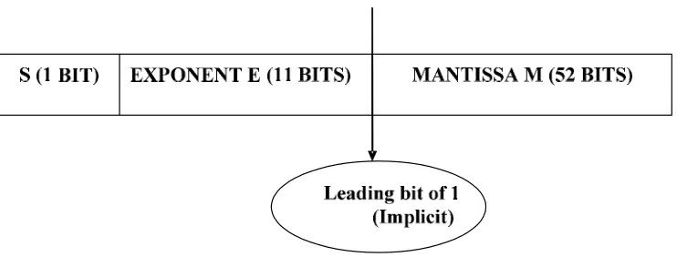
Fig 3.1 Double Precision Representation
1.F
*
1023)
-(E
*
*S
*
(-1)
X
Fig 3.2 Expression to calculate value from IEEE 754 format
The valid range of values for the exponent, mantissa and sign are shown in table 3.1.
Table 3.1 Sign, Exponent and Mantissa limits in IEEE 754 format Sign Exponent Mantissa Value /Classification
X 2047 Nonzero NaN
1 2047 zero Infinity
0 2047 zero Infinity
S 0<E<2047 Nonzero (-1)**S*2**(E-1023)*1.f
S 0 Nonzero (-1)**S*2**(-1022) *0.f
1 0 Zero 0
0 0 Zero 0
3.2 A Simple Example
Consider the number 0.15625. In order to represent it as a 64 bit number we do the following
1. Convert 0.15625 to binary which is 0.001012. This conversion can be stopped depending on the precision we require in the binary equivalent.
2. Represent the equivalent in standard notation. This becomes 1.01 * 2-3
3. Determine biased exponent by adding 1023 to original exponent .This gives 1020. 4. Mantissa is 1.01 .Make leading 1 implicit so that effective representation becomes
0 for sign bit
01111111100 for biased exponent 01 for mantissa.
5. Fill in the remaining bits of mantissa with zeros.
The following section describes the two floating point cores required for matrix multiplication. The two cores operate on each entry of the sparse matrix bringing the total number of floating point operations to twice the number of nonzeros in the sparse matrix.
3.3.1 The Floating Point Multiplier
The algorithm for double precision multiplication is based on the simple idea of multiplication of two numbers expressed in scientific notation.
Given 2 numbers A and B with A = m.decimal * 10 eA and B = n.decimal * 10 eB ,the product AB is computed by multiplication of the values m.decimal and n.decimal and addition of exponents i.e. to say that AB = (m.decimal * n.decimal) * 10 (eA + eB) .Further the product can be expressed in scientific notation if needed.
The following modules make up the multiplier: 1. Denormalizer
2. Fixed Point mantissa multiplier 3. Fixed point adder / subtractor 4. Normalizer
5. Rounding module
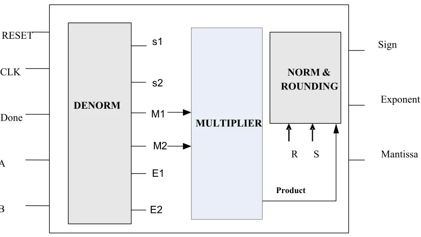
The design is fully synchronous. The top module of the multiplier is shown in Fig 4.3
3.3.1.1 Module Denormalizer
This implementation restricts itself to handling normalized values alone. More on handling denormal numbers is found in [9]. The denormalizer essentially makes the implied bit explicit. IEEE 754 format expects 52 bits of Mantissa with 1 in the 53rd bit that remains hidden and is implicit. For the purpose of multiplication the mantissa needs to be of the form 1.f. The denormalizer checks to see if the exponent of any of the operands is not zero. This is because numbers with zero exponents are unnormalized and are out of the scope of this design. The range of values that are considered normalized is provided in table 3.1.
DENORM
NORM & ROUNDING
RESET
CLK
Done
A
B
Exponent Sign
Mantissa R S
s1
s2
M1
M2
E1
E2
Product
MULTIPLIER
Fig 3.3: High level view of Floating Point multiplier core
Description of the Comparator core
The Xilinx comparator core v8.0 provides comparison logic for A=B, A<=B, A>=B, A>B, A<B and A<>B. It operates on two’s complement signed or unsigned data and can take 1 to 256 bits of input. Additionally it provides options for comparisons with a constant as well as optional clock enable synchronous and asynchronous controls for synchronous outputs. The core is shown in Fig 3.4. The depth of pipelining is constrained by the width and / or the operation being performed.[12]. For comparisons versus a constant B value of widths unto 16 bits, only two pipeline stages are possible. The degree of pipelining allowed and the corresponding operations are summarized in table 3.2.
3.3.1.2.Module Multiplier
input and a positive result for two negative inputs.
Fig 3.4 Comparator v8.0
The multiplier module also yields the sum of the two exponents and deducts the bias of 1023 from the result. There is a pipeline stage inserted between the adder and the subtractor to increase frequency. Exponent addition and subtraction is also achieved by Xilinx cores whose pipelines can be varied for increasing frequency.
Fixed Point Mantissa Multiplier
The mantissa multiplier takes two 54 bit inputs and yields a registered output that is 108 bits long. The mantissa of a 64 bit number inclusive of the hidden or the implied bit is only 53 bits long. However a 54 bit pipelined core is needed as the 53 bit core in Xilinx ISE 8.2i does not work well with overflow. Depth of pipelining of the multiplier module is dependent to a great extent on the depth of pipelining in this core. Multiplier v8.0 provides only two values; 0 for no pipelining and 1 for full pipelining and the default is 1. The latency of the multiplier will depend on the width of the two inputs A and B .The core is shown in Fig 3.5.
Comparator v8.0 A [N: 0]
B [N: 0]
SCLR CE
<OUT>
< Q_OUT>
ACLR ASET
CLK
SSET
Table 3.2: Allowable bit widths and depth of pipelines in comparator v8.0
Operation Bit width Pipelining
< Max = 256 1(+ 1 optional o/p register)
<> Max = 256 Max = 5
= Variable B >2 1
= Variable B >8 2
= Variable B >32 3
=Variable B > 128 4
= Const B > 4 1
= Const B >16 2
= Const B >64 3
<= Max = 256 1(+ 1 optional o/p register)
>= Max = 256 1(+ 1 optional o/p register)
> Max = 256 1(+ 1 optional o/p register)
ACLR SCLR
Multiplier v8.0 courtesy: www.xilinx.com
A Q
A_signed Load done
B
Load B RFD Swap B
ND
CLK RDY
Fixed Point Adder/Subtractor
The multiplier module also houses a fixed point adder/subtractor for adding the exponents and subtracting the bias from the sum. The adder/subtractor is a 11 bit core that Xilinx provides and can be readily instantiated .A pipeline stage can be inserted between the adder and the subtractor to increase frequency. The core is shown in Fig 3.6. The adder/subtractor core can create adders for A+B, subtractors for A-B or adder /subtractors that operate on both signed and unsigned data.
ADD
OVFL
C_ OUT
S[P:0]
BYPASS
CIN
D_ OVFL
D_C_OUT
D[P:0]
BYPASS
CE
ASET SSET
Q_ OVFL
Q_C_OUT
Q[P:0]
ACLR SCLR AINIT SINIT
A[N:0]
A_ SIGNED
B_ SIGNED
B[M:0]
X9078
CLK
3.3.1.3 Module Normalizer and Rounding
Once the product of the two 54 bit mantissas is obtained, we can conveniently disregard the first 2 bits for any further calculation. Our interest now lies in bits 0 through 105 as the maximum number of bits in the product of two n bit inputs is 2n. The product of a normalized floating point number with another normalized floating point number is bound to yield a value that has at most two significant digits and hence there needs to be a shift of at most two digits and a corresponding adjustment in the exponent. This uses a shifter and an exponent subtractor. A pipeline stage can be inserted between the shifter and the exponent subtractor for increasing the frequency. The shifter is clock controlled and each shift takes a single clock cycle.
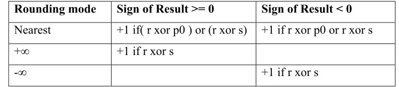
Rounding of the final value takes place to the nearest, depending on the conditions listed in table 3.3. [3]
Table 3.3 Rules for Rounding
Rounding mode Sign of Result >= 0 Sign of Result < 0
Nearest +1 if( r xor p0 ) or (r xor s) +1 if r xor p0 or r xor s
+∞ +1 if r xor s
-∞ +1 if r xor s
In table 3.3, r represents the round bit, s the sticky bit and p0 is the pth most significant bit of the result. Blanks mean that the p most significant bits of the result are the result bits themselves. If condition is true, we add one to the pth most significant bit of the result [3].
3.3.1 Floating Point Adder
The floating point adder computes the sum or the difference of two floating point numbers depending on the sign of the inputs .It uses two’s complement arithmetic to determine difference of two numbers wherever necessary.
The adder comprises the following modules: 1. Denormalizer
5. Sign
3.3.2.1 Module Denormalizer
The denormalizer has the same function as that of the denormalizer module of the multiplier. It makes the hidden bit explicit. It further unpacks the floating point numbers to its corresponding exponents, mantissas and sign bits. As mentioned in the description of the denormalizer of the multiplier, the design does not handle denormals. So the module includes a comparator core v8.0 described in section 3.3.1.1 in order to check if the exponents are zero. An additional check that the denormalizer does is to compare the two exponents with each other to determine if E1 < E2, where E1 is A’s exponent and E2 is B’s exponent. This comparison uses comparator v8.0 with certain modifications. The module encapsulates the functions of the denormalizer, 11 bit comparators for generating logical equal to and less than functions and a swapper. The 11 bit comparators can be pipelined similar to the one described in section 3.3.1.1.
The result of the comparator drives the swapper .Once the comparator outputs high, the swapper swaps the mantissas and the exponents. The exponent of the final result is always set to E1. A pipeline stage is inserted between the comparator and the multiplexer in order to increase frequency.
The signs of the two inputs are given to a two input xor gate. If the signs are different, then the two’s complement of the second operand is evaluated. There is a pipeline inserted between the evaluation of the two’s complement and the swap in case the signs are opposite. The module also needs to output the difference of the exponents in order to keep a tab on the number of shifts to get a normalized result. A 11 bit exponent subtractor determines the difference of exponents. A 11 bit subtractor core v7.0 is used for the purpose. The core is explained in 3.3.1.1. A view of the denormalizer is shown in Fig 3.7.
3.3.2.2 Module Shifter
these bits are given to the rounding module to complete the process of packing the result to the required precision. This is illustrated in fig 3.8.
Fig 3.7 Mantissa Swapping and Exponent determination in Denormalizer 3.3.2.3 Module Adder
0 1 1 0 ……….0 0 1 1 0 1
0th bit
s g
r
Fig 3.8 Bit sequence after right shift
XOR
S1 S2
MSB
C1
1
1 2C SUM
S
SUM C2
Shift right once, push in
carry out R = SUM[0]
S = g|r|s
Shift left until normalized,push
g,push 0, Exp = Exp - 1
Fig 3.9 Priority encoding in rounding module
The priority encoder operates on the sum from module adder in the following order: 1. If signs of A and B differ, MSB of sum is 1, there is no carry out then result needs
to be replaced by its two’s complement.
2. If signs of A and B are the same and there is a carry out then shift right once .Also shift the carry out into the sum.
3. Else shift left until the mantissa is normalized taking care to shift in the g bit and then zeros successively each left shift.
4. For a right shift, set rounding bit (r) to the LSB of sum before shifting. Set sticky bit is equal to OR of the guard bit, rounding bit and sticky bit.
5. If there is no shift ,set the rounding bit and guard bits to the same value ,the sticky bit to OR of round bit and sticky bit
3.3.2.5 Module Sign
The sign of the final result can be determined from the table given below. The table is implemented as a look up table. Swapped and Complemented are outputs from the denormalizer and the rounding module. Sign of the output is registered. Rounding is now done in accordance with table 3.3.
Table 3.4 Determination of sign [3]
3.4 The sparse matrix
By definition, a sparse matrix holds a large number of common values .This eliminates the need to store all the individual entries of the sparse matrix with their rows and columns .Rather, there is an enormous savings in memory if the row and column values of the uncommon entries alone can be saved. In matrix A, these common entries are all zero.
The nonzero entries are 64 bit precision values and can be stored in one of the following well known formats for sparse matrix storage.
1. Row compressed format 2. Column compressed format
Swapped Complemented SignA1 SignA2 Sign of result
Yes X + -
-Yes X - + +
No No + - +
No No - +
-No Yes + -
3.4.1 Row compressed Format
2.5 0 0 0 A = 0 1.4 0 0 0 0.9 1.23 0 0 0 0 -1.4
Fig 3.10 A sample sparse matrix
Consider the 4*4 matrix given in fig 3.10.
Nonzero entries = { 2.5 , 1.4 , 0.9 , 1.23, -1.4 } Column values for Nonzero entries = { 0 , 1 ,1, 3 }
Position index of the first nonzero in each row in the array of Nonzero = {0, 1, 2, 4}
Length of each row = {1, 1, 2, 1}
The length of each row is found from the array of position indices by subtracting the first entry from the second, the second from the third and so on. The length of the last row can be found by subtracting the last value of the array of position indices from the total number of nonzero entries in the matrix.
3.4.2 Basic Architecture
Subrow sum Accumulator Control
Unit
Down Counter
Multiplier
Multiplier Multiplier Multiplier
Number of sub rows
Zero Cu sel
Mem done
+ +
+ M
E M O R Y
Fig 3.11 A simple matrix multiplication architecture
The architecture comprises a control unit, a counter, memory, a set of floating point multiplier storage units, a binary tree of floating point adders and a sub row sum accumulator. The following sections talk more about each of these modules.
3.4.2.1 Module Descriptions Control Unit
The control unit has an enable signal that is active high. It encapsulates a divider core that determines the number of subrows in each row. The divider receives two inputs; the number of nonzeros in a given row and the number of multiplier storage units that is held constant throughout the implementation. The control unit receives these variable inputs from the test bench after the counter asserts the zero signal high. The control unit is enabled by cu sel signal which is asserted only when the zero signal is asserted low. The divider core is explained below.
Divider
writing the sum of products to the output memory or the C matrix. The divider takes in a byte long input for the divisor and dividend and yields the quotient in one clock cycle. Additional pins provided by the core include CE, SCLR, ACLR and RFD.CE refers to clock enable. CE is active high. Therefore the module retains its state when CE is deasserted. SCLR refers to Synchronous Clear. Core flip-flops used in the design of the divider can be synchronously initialized using this assert. ACLR refers to Asynchronous Clear. Core flip-flops used in the design of the divider can be asynchronously initialized using this assert. RFD refers to Ready for Data and is an indication of the cycle number at which the input data gets sampled by the core. RFD changes with the rising edge of CE if available.
Fig 3.12: Pipelined Divider v3.0
Within the core, RFD always appears at the output .However it is applicable only when an internal parameter called divclk_sel equals 1. In our design, the core is fully pipelined. The value of divclk_selwithin the IP core is set to 1. This also means that the core
samples the inputs on every enabled clock rising edge and RFD is always set to 1.
Counter
The counter is latched with an input of the total number of subrows in a given row. It steadily decrements values as well as generates memory addresses for accessing
A and B values .The counter decrements as and when the mem donesignal goes high.
Dividend RFD
Divisor Quotient
Memory
Memory is modeled as register files .The test bench populates these register files with the nonzero entries, their column values and the number of nonzero entries per row. The primitive $readmemh allows hex values to be read off the file and dumped into register files. The register file of nonzero values is 64 bits long and holds about 256 values. The bit widths held in the other two register files is dependent on the maximum length of rows that the sample file holds.
Multiplier
Each of these units receives the 2 floating point numbers to be multiplied .This is the floating point multiplication core that was discussed earlier. The number of multiplier units that need to be operated in parallel is dependent on the sparsity structure of the matrix. Analysis of sparsity structure of matrix requires detailed statistics about the matrix and the number of nonzero entries. Also the number of Floating point units that can be configured on the FPGA is limited by the available resources. This
implementation does not depend on the sparsity structure of the matrix
In order to input two double precision values to the multiplier the FPGA chosen must atleast accommodate 128 input pins. Simulation on devices that are constrained by IOBs or input output ports are bound to report an warning during synthesis and a subsequent error during mapping and translation onto the FPGA.
Binary tree of adders
The outputs from the multipliers are fed into a binary tree of adders. Each of these adders is the double precision core described earlier. Two of the four products go into the nodes of the tree .It is to be noted that the total number of leaf nodes is only four. So the tree has three levels. The root node of the tree passes the cumulative sum of products from one sub row only. Therefore this module does not keep a tab on the number of subrows whose products and sums have been calculated.
Sub row Sum Accumulator
If the size of each row is k, then the sum accumulator is not required as the root node itself yields the final result. However the values are still allowed to pass through the accumulator to maintain the simplicity of implementation.
Chapter 4
Verification
Design verification is defined as the reverse process of design. It takes in an implementation as an input and confirms that the implementation meets the specifications. Though design verification includes functional verification, timing verification, layout verification and electrical verification, functional verification is by default termed design verification.
Two popular forms of verification are the simulation based approach and the formal verification approach. The most important difference between the two approaches is that simulation based approaches need input vectors while formal verification approaches do not. In the former, we generate input vectors and derive reference outputs from them. However a formal verification approach differs in that it predetermines what output behavior is desirable and uses the formal checker to see if it agrees or disagrees with the desired behavior. This shows that simulation based approach is input driven while formal approach is output driven. Since formal verification methodology operates on an input space as against chosen vectors, it can be more complete. Simulation based approach takes a point in the input space at a time and therefore samples few points only. However, this can be justified due to the extensive use of memory and long runtime that formal verification uses. Besides when memory overflow is encountered, the tools are at a loss to show what is the right problem and its fix. [7]
The design is also checked with variable exponents. This is done in order to check the alignment of the two exponents in favor of the larger. This check is important because it checks the functionality of the shifter. The design is capable of handling only normalized inputs. A check for denormalized inputs is already embedded in the design. However we need to verify if the accelerator gracefully terminates with zero outputs when such inputs are given.
The Normalizer or the priority encoder is the main part of the module that prepares the adder for rounding and sign determination. This module needs to be completely verified. Hence inputs are so designed that each case in the priority encoder gets exercised. Verification of this module covers a large number of values from the input space.
Chapter 5
Results
This chapter discusses results and interpretations from simulation and synthesis of the floating point cores. It throws light on the tradeoffs made in various points in design as well as a few nuances of FPGA design that come to fore during emulation.
5.1 Simulation
This design has been implemented using Xilinx ISE 8.2i, simulated on ModelSim 6.1i and synthesized using XST for Verilog. The HDL code uses Verilog 2001 constructs that provide certain benefits over the Verilog 95 standard in terms of scalability and code reusability. Simulation based verification is one of the methods for functional verification of a design. In this method, test inputs are provided using standard test benches. The test bench forms the top module that instantiates other modules. Simulation based verification ensures that the design is functionally correct when tested with a given set of inputs. Though it is not fully complete, by picking a random set of inputs as well as corner cases, simulation based verification can still yield reasonably good results.
The following snapshots are taken from ModelSim 6.1 after the timing simulation of the adder and multiplier cores.
Consider the inputs to the floating point adder. A = -1.25
B = 1.5
The inputs to the adder were the corresponding hex values obtained from [13]. A = 64’hBFF4000000000000
B = 64'h3FF8000000000000
The output of the adder should be 0.25 .After regrouping the bits from the resulting 64 bit number; the sum is interpreted.
From fig 5.1 ,the sign of the result is 0 ,mantissa is 1 followed by 0…….1011011,a total of 53 bits and the exponent after subtracting the bias gives -2.This implies
Fig 5.1 Simulation results from adder
Let us now consider two inputs to the multiplier. A = 1.0
B = -1.3
Expected product = -1.3
Product = -1.3000000000000003
The results from simulation are provided in Fig 5.2. On regrouping the sign, mantissa and the exponent we obtain -1.3000000000000003.
5.2 Synthesis
effort, area goal, timing goal, resource sharing, register retiming etc. The synthesis tool provides default settings for optimum performance over generalized applications. A large portion of the synthesis uses these default settings.
There are certain applications that may require customization of these settings but caution should be exercised. A typical example would be resource sharing for reducing gate count ,but resource sharing cannot be used in timing critical paths.
Fig 5.2 Simulation results from the multiplier
There are two methods to improve performance of design. One is to assist the synthesis tool in identifying critical logic blocks by use of timing constraints. The other method involves writing a code that gives the synthesis tool an easier problem to solve. This also means use of pipelines or fast structural elements to implement logic.
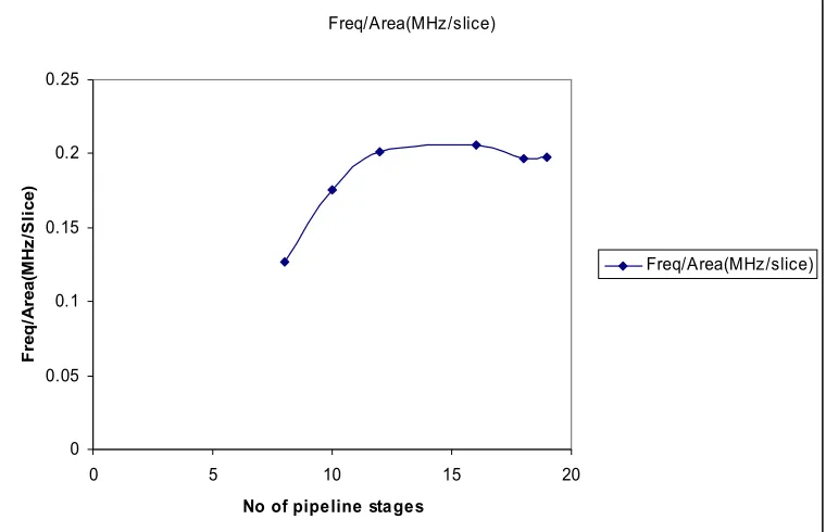
One of the most important metrics to determine performance of a hardware accelerator is throughput. In general, pipelining is one of the most effective methods to improve throughput. It is found through synthesis that the depth of pipeline directly affects throughput. Pipelining offers an overall saving in time for execution of all instructions put together. It does not affect individual instruction time. However the flipside to pipelining in use of increased resources and a subsequent increase in area. Since throughput is a ratio of clock speed and area, it is necessary to strike a fine balance so as to be able to maintain high throughputs. For this reason, it is often necessary to play around with values at both ends of the clock speed and area spectrum until a point of diminishing returns is reached.
Table 5.1 Variation of Freq/Area with pipelining for 64 bit multiplier
A sample of the timing report and device utilization summary generated using XST is shown below. The report was generated for maximum pipelining.
* Final Report *
No of pipelines (adder )
Area (Slices)
Clock Rate (MHz)
Freq/Area (MHz/slice)
Minimum 424 65.996 0.1556
Device utilization summary:
---Selected Device: 2vp40fg676-7
Number of Slices: 1956 out of 19392 10% Number of Slice Flip Flops: 3405 out of 38784 8% Number of 4 input LUTs: 3480 out of 38784 8% Number used as logic: 3292
Number used as Shift registers: 188 Number of IOs: 195
Number of bonded IOBs: 195 out of 416 46% Number of GCLKs: 1 out of 16 6%
=============================================================== TIMING REPORT
Clock Information:
---+---+---+ Clock Signal | Clock buffer (FF name) | Load | ---+---+---+ Clock | BUFGP | 3593 | ---+---+---+
Asynchronous Control Signals Information:
---No asynchronous control signals found in this design Timing Summary:
---Speed Grade: -7
Minimum period: 5.663ns (Maximum Frequency: 176.585MHz) Minimum input arrival time before clock: 3.224ns
Maximum output required time after clock: 3.340ns Maximum combinational path delay:
---A comparison of throughputs between earlier implementations and ours is shown in table 5.2.
Table 5.2 Comparison of results from the synthesis of multiplier
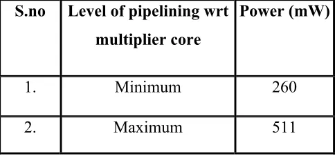
Total power consumed can also be estimated in Xilinx ISE 8.2i using XPower. Table 5.3 tabulates power for minimum and maximum pipelining in the multiplier core. Xilinx XPower is a power analysis software tool. It uses device knowledge and design data to estimate device power and power utilization in the nets. [13].
Table 5.3 Power vs. pipelining for 64 bit multiplier
S.no Level of pipelining wrt multiplier core
Power (mW)
1. Minimum 260
2. Maximum 511
Synthesis results from 64 bit adder
The double precision adder core is also synthesized using Xilinx XST. The details from the device utilization summary and timing reports for various levels of pipelining are captured in table 5.4.
PRECISION 64 BITS
NCSU USC NEU
Area (slices) 964 910 477
Clock Rate (MHz/slice)
176.585 205 90
Freq/Area (MHz/slice)
Table 5.4 Synthesis results from 64 bit adder
A comparison between our implementation and previous implementations has been drawn and summarized in table 5.5 and table 5.6. In table 5.5, Opt stands for optional which denotes highest frequency/area ratio. This is because we investigate tradeoffs in frequency and area by extensively pipelining the core until we reach the point of
diminishing returns. The Max value in the table captures this precisely. There is no point in increasing the depth of pipelines beyond the point of diminishing returns.
Table 5.5 Comparison of minimum, maximum and optimal metric for adder
No. of Pipeline
Stages
Area (slices)
LUTS Flip flops Clock Rate (MHz)
Freq/Area MHz/slice
12 876 1075 1168 176.177 0.2011
16 877 1097 1168 180.442 0.2057
18 924 1042 1182 182.121 0.197
19 930 1100 1183 184.312 0.198
USC NCSU
Precision
64 bits Min Max Opt Min Max Opt
Pipelines 6 21 19 8 19 16
Area (slices) 633 1133 933 548 930 877
LUTS 1049 1032 976 976 1100 1097
Flip flops 443 1543 1148 598 1183 1168
Clock (MHz) 50 220 200 69.97 184.3 180.4
Freq/Area MHz/slice
Table 5.6 Table of metric comparisons for 64 bit adder
Experimental results from USC and NEU are provided in [4] and [8]. Relation between the depth of pipelines and throughput is shown in Fig 5.4. Table 5.7 captures the variation of power as measured on Xpower with pipelining. The Xilinx Synthesis tool translates, maps and does a place and route for a design after which it uses XPower to computer the total power consumed by the device. Power measurements are summarized in table 5.7 and the variation is graphically captured in Fig 5.3.
Metric NCSU USC NEU
No of pipeline stages
16 19 8
Area (slices) 877 933 770
Clock Rate (MHz)
180.4 200 54
Freq/Area (MHz/slice)
Table 5.7 Variation of power with pipelining in 64 bit adder
Fig 5.3 Variation of power with pipelines in 64 bit adder S.no No of
pipelines
Power (mW)
1 8 360
2 10 355
3 12 420
4 16 420
5 18 477
6 19 510
Power(mW) vs Pipeline stages
0 100 200 300 400 500 600
0 5 10 15 20
No of pipe line s
P
ow
er
(m
W
)
Fig 5.4 Variation of freq/area vs. pipelines in 64 bit adder
The placed and routed design for the multiplier and adder are shown in Fig 5.5 and Fig 5.6. Xilinx ISE 8.2i provides means to implement the design and realize it on the FPGA by providing functions for translation, mapping and finally place and route. Let’s take the case of the multiplier. The report from the place and route tool states that about 9% of the area has been utilized. Since area is not a big constraint here, we can focus more on timing related constraints more and try to improve the frequency of operations through more pipelining. But for every application, it’s a question of whether an addition in time or area is really affordable or not. The design needs to be tweaked in accordance with such a requirement. The choice of the FPGA is crucial during the synthesis of the design. In case of a 64 bit operation, be it a multiplier or an adder, it only makes sense to have atleast 64 input ports and better still 128 for two inputs to be fed to the device. Often times during synthesis, if the device utilization summary reports “more than 100% of resources are being used” or anything similar, it only makes sense to upgrade to a higher
Freq/Area(MHz/slice)
0 0.05 0.1 0.15 0.2 0.25
0 5 10 15 20
No of pipeline stages
F
re
q
/A
re
a
(M
H
z
/S
li
c
e
)
device, since we do not want to be constrained with regard to fundamental resources on a board.
Fig 5.6 Snapshot of the 64 bit adder after place and route
Chapter 6
Conclusion and Future Work
Double precision floating point arithmetic significantly increases the levels of precision when compared to single precision floating point or integer arithmetic. However there might be situations where double precision calculation results in a numerically unstable solution. This could mean that double precision is insufficient to obtain an accurate result. In such a case, quadruple or multiple precision floating point arithmetic can be used. A typical example is a Bessel function calculation J1(x) for |x| up to a few hundreds. Though it is a convergent series for small values of x, in case of large values, the result is unstable. The final sum of the series is often 10-15 orders lower in magnitude than the intermediate sum which reduces confidence in any of the digits in the final sum. [14].
Though we have implemented a basic architecture for matrix multiplication using the double precision cores, as an extension, it is possible to implement advanced architectures for handling very large sparse matrices with refinement in the sum accumulator and at the cost of hardware complexity. Further the algorithm for sum and product computations can be extended to the implementation of more complex arithmetic or better precision arithmetic with the use of quadruple precision or multiple precision floating points.
References
[1] Z. Guo, W. Vahid, and K. Vissers,“Quantitative Analysis of the Speedup Factors of
FPGAs over Processors”, Proceedings of the 2004 ACM / SIGDA 12th international
symposium on Field--programmable gate arrays, Monterey, CA, February 2004.
[2] S. Craven, C. Patterson, and P. Athanas, “Super-sized Multiplies: How Do FPGAs Fare in Extended Digit Multipliers?”, Proceedings of the 7th Annual Conference on
Military and Aerospace Programmable Logic Devices, Washington DC, September 2004.
[3] J.L. Hennessey, D.A. Patterson, Computer Architecture, A Quantitative Approach, Morgan Kaufmann, Third Edition; 2002.
[4] G. Govindu, L. Zhuo, S. Choi, V. Prasanna, “Analysis of high-performance floating point arithmetic on FPGAs”, Proceedings of 18th International Parallel and Distributed
Processing Symposium, April 2004.
[5] IEEE standard for binary-floating point arithmetic, ANSI/IEEE Std 754-1985, The Institute of Electrical and Electronic Engineers Inc., New York, August 1985.
[6] L. Zhuo, V.K. Prasanna, “Sparse Matrix Vector Multiplication of FPGAs”,
Proceedings of the 2005 ACM / SIGDA 13th international symposium on
Field-programmable gate arrays, Monterey, CA,February 2005.
[7] W.K. Lam, Hardware Design Verification, New Jersey; Prentice Hall, 2005.
[8] P. Belanovic, M. Lesser, “A Library of Parameterized Floating Point Modules and their use”, Proceedings of 12th International Conference on Field Programmable Logic
[9] E.M. Schwarz, M. Schmookler, S. Trong, “Hardware Implementation of
Denormalized Numbers.” Proceedings of 16th IEEE Symposium on Computer Arithmetic,
June 2003.
[10] K. Coffman, Real world FPGA Design with Verilog, New Jersey; Prentice Hall,
2000.
[11] M.R. Shah, “Design of a self-test vehicle for ac coupled interconnect technology”, Master’s thesis, NC State University, March 2005.
[12] Comparator v8.0, User guide, Xilinx Incorporation.
[13] XPower, Web Power tools User guide, Xilinx Incorporation.
[14] D.M. Smith, “Using multiple precision arithmetic”, Computing in Science and
Engineering, vol.5, no.4, August 2003.
APPENDIX
APPENDIX A
Verilog HDL for Multiplier and Adder Cores
VERILOG HDL FOR MULTIPLIER
TEST BENCH FOR 64 BIT MULTIPLIER
`timescale 1ns / 1ps
//////////////////////////////////////////////////////////////////////////////////////////// // Company : North Carolina State University
// Engineer : Yasaswini Sudarsanam //
// Module Name: Rounding
// Project Name: Double precision floating point arithmetic cores (Multiplication) // Device : Xilinx Virtex 2 pro - XC2VP20
// Description : Testbench for multiplier core //
// Ports : None //
// Sub modules: topmult //
// Revision : 0.01 - File Created (9/15)
// 0.02 - Variation in test inputs from here on
// 0.03 - Creation of topmult to encapsulate all submodules.Elimination of // sub modules from the test bench
//
//////////////////////////////////////////////////////////////////////////////////////////// module test();
reg clock; reg done; reg reset;
reg [63:0] floatA; reg [63:0] floatB;
wire [51:0] final_product; wire [10:0] exp_sumAB; initial
clock = 1'b0; always
#5 clock = ~clock;
topmult t1(clock,reset,done,floatA,floatB,final_product,exp_sumAB,sign_A_B); initial
begin
floatB = 64'hBFF4CCCCCCCCCCCD; done = 1;
reset = 1; #10 reset = 0; end
endmodule
TOP MODULE FOR MULTIPLIER
`timescale 1ns / 1ps
//////////////////////////////////////////////////////////////////////////////////////////// // Company : North Carolina State University
// Engineer : Yasaswini Sudarsanam //
// Module Name: Rounding
// Project Name: Double precision floating point arithmetic cores (Multiplication) // Device : Xilinx Virtex 2 pro - XC2VP20
// Description : Topmodule for multiplier. Encapsulates the denormalizer, multiplier // and rounding modules
// Ports : Clock - Clock input // reset - Synchronous Reset // floatA - 64 bit multiplicand // floatB - 64 bit multiplier
// final_product - Product after rounding // exp_sumAB - exponent after rounding // sign_A_B - Sign of product
//
// Submodules: None //
//
// Revision : 0.01 - File Created (9/9) //
//
////////////////////////////////////////////////////////////////////////////////////////////
module topmult(clock,reset,done,floatA,floatB,final_product,exp_sumAB,sign_A_B); input clock;
input done;
input [63:0] floatA; input [63:0] floatB; input reset;
wire sign_bitA; wire sign_bitB;
wire [10:0] exponentA; wire [10:0] exponentB; wire denormalized; wire [107:0] productAB; wire [10:0] exponent_sum; wire prod_done;
output [51:0] final_product; output [10:0] exp_sumAB; output sign_A_B;
wire sign_A_B; wire reset;
wire [51:0] final_product; wire [10:0] exp_sumAB; denorm d1(clock,reset,done,floatA,floatB,sign_bitA,sign_bitB,mantissaA,mantissaB,exponentA,e xponentB,denormalized); multiplier m1(clock,reset,denormalized,sign_bitA,sign_bitB,mantissaA,mantissaB,exponentA,expo nentB,productAB,exponent_sum,sign_A_B,prod_done); rounding r1(clock,reset,productAB,exponent_sum,prod_done,final_product,exp_sumAB); endmodule MODULE DENORMALIZER `timescale 1ns/1ps //////////////////////////////////////////////////////////////////////////////////////////// // Company : North Carolina State University
// Engineer : Yasaswini Sudarsanam //
// Module Name: Rounding
// Project Name: Double precision floating point arithmetic cores (Multiplication) // Device : Xilinx Virtex 2 pro - XC2VP20
// Description : Topmodule for multiplier. Encapsulates the denormalizer, multiplier // and rounding modules
// Ports : Clock - Clock input // reset - Synchronous Reset
// done - Handshaking signal with an external module whose logic includes this // core
// floatA - 64 bit multiplicand // floatB - 64 bit multiplier // sign_bit1 - 1 bit sign of A // sign_bit2 - 1 bit sign of B
// extended to 54 bits for ease of use with Xilinx core // exponent1 - 11 bit exponent of floatA
// exponent2 - 11 bit exponent of floatB
// denormalized - 1 bit assertion to denote end of operations in the denormalizer // final_product - Product after rounding
// exp_sumAB - exponent after rounding // sign_A_B - Sign of product
//
// Submodules: Constant Port B comparator// //
// Revision : 0.01 - File Created (9/9) // // //////////////////////////////////////////////////////////////////////////////////////////// module denorm(clock,reset,done,floatA,floatB,sign_bit1,sign_bit2,mantissa1,mantissa2,exponent 1,exponent2,denormalized); input clock; input done; input reset;
input [63:0] floatA; input [63:0] floatB; output sign_bit1; output sign_bit2;
output [53:0] mantissa1; output [53:0] mantissa2; output [10:0] exponent1; output [10:0] exponent2; output denormalized; reg sign_bit1;
reg sign_bit2;
reg [10:0] exponent1; reg [53:0] mantissa1; reg [10:0] exponent2; reg [53:0] mantissa2; reg [10:0] zero_reg; wire qA1;
wire qA2;
reg denormalized;
comp c1(qA1,clock,floatA[62:52]); comp c2(qA2,clock,floatB[62:52]); always @(posedge clock)
begin
begin
sign_bit1 <= floatA[63]; sign_bit2 <= floatB[63]; exponent1 <= floatA[62:52]; exponent2 <= floatB[62:52]; mantissa1 <= {1'b1,floatA[51:0]}; mantissa2 <= {1'b1,floatB[51:0]}; denormalized <= 1;
end end else begin
mantissa1 <= 54'b0; mantissa2 <= 54'b0; exponent1 <= 11'b0; exponent2 <= 11'b0; sign_bit1 <= 1'b0; sign_bit2 <= 1'b0; denormalized <= 1'b0; zero_reg <= 11'b0; end
end
endmodule
MODULE MULTIPLIER `timescale 1ns / 1ps
//////////////////////////////////////////////////////////////////////////////////////////// // Company : North Carolina State University
// Engineer : Yasaswini Sudarsanam //
// Module Name : Rounding
// Project Name: Double precision floating point arithmetic cores (Multiplication) // Device : Xilinx Virtex 2 pro - XC2VP20
// Description : Topmodule for multiplier. Encapsulates the denormalizer,multiplier // and rounding modules
//
// Ports : Clock - Clock input // reset - Synchronous Reset // denormalized - Enable signal // floatA - 64 bit multiplicand // floatB - 64 bit multiplier // sign_bitA - 1 bit sign of A // sign_bitB - 1 bit sign of B
// extended to 54 bits for ease of use with Xilinx core // mantissaB - 53 bit mantissa of floatB, includes implicit 1 , // extended to 54 bits for ease of use with Xilinx core // exponentA - 11 bit exponent of floatA
// exponentB - 11 bit exponent of floatB
// prod_done - 1 bit assertion to denote end of operations in the multiplier // productAB - Mantissa product
// exponent_sum - exponent after multiplication // sign_A_B - Sign of product
//
// Submodules: 54 BIT MULTIPLIER CORE //
//
// Revision : 0.01 - File Created (9/9) // // //////////////////////////////////////////////////////////////////////////////////////////// module multiplier(clock,reset,denormalized,sign_bitA,sign_bitB,mantissaA,mantissaB,exponent A,exponentB,productAB,exponent_sum,sign_A_B,prod_done); input clock; input denormalized; input reset; input sign_bitA; input sign_bitB; output sign_A_B; input [10:0] exponentA; input [10:0] exponentB; input [53:0] mantissaA; input [53:0] mantissaB; output [107:0] productAB; output [10:0] exponent_sum; output prod_done;
reg [10:0] exponent_sum; reg sign_A_B;
reg [11:0] exp_temp; wire [107:0] productAB; reg prod_done;
mult m1(clock,mantissaA,mantissaB,productAB);
always@ (posedge clock)
if(!reset) begin
//This addition is replaced by the 11 bit Xilinx core exp_temp = exponentA + exponentB;
//While experimenting with number of pipelines ,
//this subtraction can use a core and be pipelined with addition from above exponent_sum <= exp_temp - 1023;
end
sign_A_B <= sign_bitA ^ sign_bitB; prod_done <= 1;
end else
begin
prod_done <= 0; sign_A_B <= 0; end
endmodule
MODULE ROUNDING
`timescale 1ns / 1ps
//////////////////////////////////////////////////////////////////////////////////////////// // Company : North Carolina State University
// Engineer : Yasaswini Sudarsanam // Module Name: Rounding
// Project Name: Double precision floating point arithmetic cores (Multiplication) // Device : Xilinx Virtex 2 pro - XC2VP20
// Description : This module takes care of rounding the product to the nearest // Ports : clock - Clock input
// reset - Synchronous Reset
// productAB - product of mantissas // exponent_sumAB - Exponent sum
// prod_done - module enable signal that says product calculation is done and // rounding can begin
// final_product- Rounded product // exp_sum - Exponent after rounding //
//
// Submodules: None //
//
// Revision : 0.01 - File Created (9/9) //
//