Encryption on Field-Programmable Gate
Arrays
K.Tagore, P.Venkatesh, K.Mary supreethi
Assistant Professor, Dept. of ECE, CIET, LAM, India
Dept. of ECE, CIET, LAM, India
Dept. of ECE, CIET, LAM, India
ABSTRACT- This paper presents two designs for the advanced encryption standard on field-programmable gate arrays (FPGAs) which occupies low area. The first design is an 8-bit application-specific instruction processor, which supports key expansion (currently programmed for a 128-bit key), encipher and decipher. The design utilizes less than 60% of the resources of the smallest available Xilinx Spartan II FPGA (XC2S15). The average encipher-decipher throughput is 2.1 Mbps when clocked at 70 MHz. The design has numerous applications where low area and low power are priorities. The second design, using the Xilinx PicoBlaze soft core is included to provide an embedded 8-bit microcontroller comparison baseline.
KEYWORDS: advanced encryption standard (AES), application-specific instruction processor (ASIP), field-programmable gate array (FPGA).
I. INTRODUCTION
In January 1997, the National Institute of Standards and Technology (NIST) set out to establish a new standard of cryptographic algorithm to protect sensitive computer information and telecommunications systems in the Federal Government. The new algorithm would replace the aging Data Encryption Standard (DES) cipher algorithm, developed by IBM in the early 1970’s. As a FIPS standard, AES will officially be identified as an approved cipher algorithm that can be used by U.S. Government organizations to protect sensitive (unclassified) information. Those Government organizations will be able to use the other FIPS approved algorithms in addition to, or in lieu of, AES.
The AES and its implementation for both application-specific instruction processor (ASIC) and field-programmable gate array (FPGA) technologies has been the subject of much research and continues to be a topic of interest in both academic and commercial environments.
In recent years, there has been a trend towards using FPGA in the production versions of electronic systems. It is no longer true that FPGAs are only used for prototyping. Their inclusion in the final version, would at first appear more expensive, however the ability to update the design and reduced time to market are strong commercial drivers. This was furthered by the introduction by the FPGA manufacturers of effectively mask programmed standard-cell versions of their technologies. This has resulted in an increased demand on optimal FPGA designs.
II. ASIP DESIGN
The first decision was to select an appropriate datapath width for the processor. As already described in the introduction, a number of the previous low-resource designs had opted for a 32-bit datapath. Examination of the AES mathematics revealed the possibility of using an 8-bit datapath which had not been previously explored. Using less than 8 bits is believed to be impractical as the AES predominately uses 8-bit Galois Field arithmetic.
The design of the ASIP was an iterative process. The design was conceptually split into three principal areas: the hardware, the instruction set and the application program. The definition of the instruction set effectively formed a design partition between the software and hardware aspects. A number of design iterations were followed. This is the classical hardware-software co-design issue.
From the initial stages of the design, three key issues were identified which contributed to most of the area. The first concerned the computation of SubBytes, for which existing implementations vary from look-up tables to computing the function mathematically. The second, was the definition of a suitable primitive operation (namely ffm-accumulate) to efficiently perform the Galois Field mathematics in the AES MixColumns, AddRoundKey, and KeyExpansion operations. The final issue was program ROM size reduction for which the two traditional techniques of iteration and subroutines were considered. These three issues are discussed in detail in the following sections.
A. Low-Area SubBytes
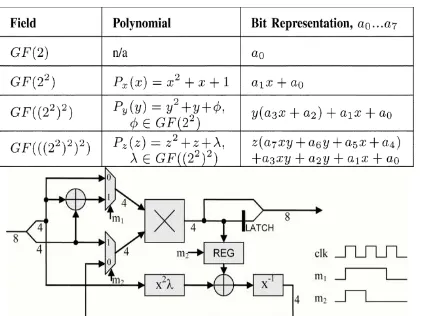
The most obvious method for implementing the SubBytes operation on FPGA was using a look-up table (LUT) based around a block memory (the “S-box”). The table for the forward and inverse transformation would require 512 bytes (4kbits). Given the dual port nature of Xilinx block memories this ROM could be used for two simultaneous operations. Here, an alternative, lower area, solution was required. A number of existing works [1]–[10] demonstrated how Sub-Bytes may be computed using Composite Field mathematics rather than a LUT.In order to perform an equivalent inversion in composite field arithmetic additional isomorphic transformations are required. These can be found using the method described in Paar [7]. The composite field theory was applied a number of times to construct a set of fields starting with the base field and building up successively to reach. Each stage has its own primitive trinomial and binary value format. Table I summarizes the field construction.
The objective was to perform the multiplicative inverse of the supplied value in GF(((22)2)2) over a number of cycles sharing the composite field multiplier. Here, the input byte is split into two 4-bit nibbles V=Az + B.
TABLE I: COMPOSITE FILD ARITHMETIC
Fig.1 Block diagram of multiplicative inverse in GF(((2)2)2)2)
needed to perform the AES) this would have unduly limited the performance. Thus, SubBytes was split further into a total of five cycles to remove it from the critical path.
Fig.2 Block diagram of new subbytes circuit
This approach reduced the total forward and inverse SubBytes circuit to 42 slices on an XC2S15, a reduction in size of 27% compared to the original high-throughput version [9].
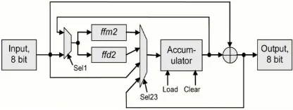
B. 8-BitffmAccumulate
The AES MixColumns operator is fundamentally a 32-bit and there have been a number of designs [5][6] based around a 32-bit datapath. Only one design [9], for ASIC, was found which reported using an 8-bit datapath. However, the design married a 32-bit MixColumns to the 8-bit datapath by successively loading three 8-bit input registers in sequence to form the required 32-bit word with a similar process at the output. Here, a truly 8-bit alternative is sought with the corresponding area saving.
Examining the AES algorithm, a set of primitive operations were determined which cover the remaining operations of ShiftRows, mixColumns, and KeyExpansion. These were found to be ffm2 and XOR. For this design, the decipher function was also required and as it is undesirable to store the entire set of RoundKeys, a further operation of finite-field halving or finite-field division by two (ffd2) was needed for reverse KeyExpansion. The ShiftRows operator was implemented as a set of 8-bit data moves between memory locations. There are numerous examples in the MixColumns and Key-Expansion calculations where the result of an 8-bit operation was further acted upon. This was either in terms of repeated finite-field addition or repeated ffm2s. Thus, the inclusion in the datapath of an accumulator reduced the demands placed on the data memory. These requirements led to the development of a multiply-accumulate architecture capable of supporting moving 8-bit data 8-bit finite-field addition (XOR) and multiplication and division by two in GF(28). An execution unit specific to this type of operation was developed and its circuit is presented in Fig.
Fig. 3 Circuit diagram for “multiply-accumulate” functions.
C. Program ROM Size Reduction
One of the critical design decisions was which looping constructs, if any, were to be supported. A very simple processor could be constructed which only permitted execution of linear code. However, once the cost of the large program ROM size was balanced against the area and performance penalties for implementing even the most limited forms of iteration then linear code was no longer a viable option. The standard techniques for reducing the size of a program are iteration and subroutines. However, both techniques require specialist support from the processor hardware thus their inclusion would increase the area cost and complexity of the processor.
III. ASIP HARDWARE
TABLE 2: PROCESSOR INSTRUCTION SET
Fig.3 ASIP Architecture
The complete instruction set for the processor is summarized in Table II. Fig. shows the architecture of the processor. It should be noted that due to the clocking requirement of block memories, instructions take multiple cycles.
IV. ASIP SOFTWARE
a. Forward Key Expansion
The key expansion, defined in the AES specification, can express as a set of operations which are performed each round to generate the next RoundKey.
Fig.4: Forward Key Expansion.
b. Reverse Key Expansion
Reverse key expansion was approached using a similar method to the forward key expansion. However, the process starts
with (
k
3 , 7 , 11 , 15
'k
'k
'k
') and works backwards to finally yield (k
0 , 4 , 8 , 12
'k
'k
'k
' ). This time the Rcon value was propagated in the reverse direction using ffd2.V. RESULTS
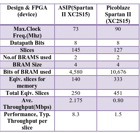
Fig.4&5 shows that the placement of this design fits comfortably into the smallest Spartan-II device (XC2S15) occupying about 60% of the resources. The design required 145 slices (depending on user constraints) and two block memories. The block memory used as the register file was only partially utilized (360 bits) which gives rise to an alternative implementation using distributed memory with a cost of 42 additional slices and saving one of the block memories. No comparable 8-bit FPGA designs were found so comparison was made against the best 32-bit designs. Additionally, a second design was developed using the freely available Xilinx PicoBlaze core. This was done to provide a small embedded software baseline for comparison in terms of throughput and area. A concession was made in terms of implementing SubBytes as a ROM based lookup table.
Fig.6 Placement on XC2S15 FPGA
TABLE 3: IMPLEMENTATION RESULTS
Design & FPGA (device)
ASIP(Spartan II XC2S15)
Picoblaze Spartan II
(XC2S15) Max.Clock
Freq.(Mhz)
73 90
Datapath Bits 8 8
Slices 145 127
No.of BRAMS used 2 2
BRAM Size 4 4
Bits of BRAM used 4,580 10,676
Eqiv. slices for memory
140 333
Total Eqiv. Slices 250 451
Ave. Throughput(Mbps)
2.175 0.80
Performance, Typ. Throughput per
slice
VI. CONCLUSION
Both the ASIP and PicoBlaze based designs are the smallest known FPGA implementations to date. Such designs have application across a wide range of areas especially those needing a short time to market and relatively low power.
REFERENCES
[1] X. Zhang and K. K. Parhi, “High-speed VLSI architectures for the AES algorithm,” IEEE Trans. Very Large Scale Integr. (VLSI) Syst., vol. 12, no. 9, pp. 957–967, Sep. 2004.
[2] A. Hodjat and I. Verbauwhede, “A 21.54 Gbits/s Fully Pipelined AES Processor on FPGA,” in Proc. FCCM’04, Apr. 2004, pp. 308–309. [3] J. Zambreno, D. Nguyen, and A. Choudhary, “Exploring Area/Delay Trade-Offs in an AES FPGA Implementation,” in Proc. LNCS FPL’04,
Antwerp, Belgium, 2004, vol.3203,pp.575-585.
[4] P. Chodowiec and Gaj, “Very Compact FPGA Implementation of the AES Algorithm,” in Proc. LNCS’03,2003,vol.2779,pp.319-333. [5] G. Rouvroy F. X. Standaert, J. J. Quisquater, and J. D.Legat,“ Compact and efficient encryption/decryption module for FPGA implementation of
the AES Rijndael very well suited for small embedded applications,” in Proc. ITCC’04, Apr. 2004, vol. 2, pp. 583–587.
[6] V. Fischer and M. Drutarovsky, “Two Methods of Rijndael Implementation in in Reconfigurable Hardware,” in Proc. CHES’01, 2001, vol. 2162, pp. 77–92.
[7] F. X. Standaert, G. Rouvroy, J. Quisquater, and J. Legat, “A Methodology to Implement Block Ciphers in Reconfigurable Hardware and its Application to Fast and Compact AES RIJNDAEL,” in Proc. ACMFPGA’03, Monterey, CA, 2003, pp. 216–224.
[8] M. Feldhofer, S. Dominikus, and J. Wolkerstorfer, “Strong Authention for RFID Systems Using the AES Algorithm,” in Proc. LNCSCHES’04, 2004, pp. 357–370.
[9] A. Satoh, S. Morioka, K. Takano, and S. Munetoh, “A Compact Rijndael Hardware ArchitectureWith S-Box Optimization,” in Proc. LNCSASIACRYPT’01, Dec. 2001, vol. 2248, pp. 239–254.