STUDY THE EFFECTS OF ELECTROMAGNETIC BAND-GAP (EBG) SUBSTRATE ON TWO PATCHES MICROSTRIP ANTENNA
H. F. Shaban, H. A. Elmikaty, and A. A. Shaalan
Zagazig University Cairo, Egypt
Abstract—Utilization of electromagnetic band-gap (EBG) structures
is becoming attractive in the electromagnetic and antenna community. In this paper, the effects of a two-dimensional electromagnetic band-gap (EBG) Structures on the performance of microstrip patch antenna arrays are investigated using the Ansoft High Frequency Selective
Simulator (HFSSTM). A mushroom-like EBG structure is compared
with 2-DEBG Structures. HFSSTM is employed to determine the
effects of different Structures on two element microstrip patch antennas
array. Two element microstrip patch antenna array on a uniform
substrate suffer from strong mutual coupling due to the pronounced surface waves. Therefore, diverse forms of 2-DEBG Structures like: little number of holes, large number of holes, defect mode and different number of mushroom-patches columns structure are discussed. The two element microstrip patch antennas array placed on a defect in the electromagnetic (EBG) substrate that localizes the energy under the antennas. The excitation frequency of the two element microstrip patch antennas array near the resonance frequency of the defect mode can be used to control the coupling between antennas that are placed in an array. The mutual coupling improved by using large number of mushroom-patches columns structure.
1. INTRODUCTION
In recent years, a new technology has emerged which may be
the key to developing ultra-wideband microstrip antennas. This
electromagnetic interference levels. These substrates contain so-called Photonic Crystals. Also known as electromagnetic band-gap (EBG) structures and electromagnetic band-gap materials (EBMs), are a class of periodic metallic, dielectric, or composite structures that exhibit a forbidden band, or bandgap, of frequencies in which waves incident at various directions destructively interfere and thus are unable to propagate [1, 2]. Based on the dimensional periodicity of the crystal structure, the bandgaps can be in one, two, or three-dimensional planes, with the level of complexity increasing
as the dimensions increase. The first photonic-crystal structure
conceptualized and manufactured was in 1991 by Yablonovitch, then at Bell Communications Research in New Jersey. Yablonovitch fabricated the crystal structure by mechanically drilling holes a millimeter in diameter into a high dielectric constant material [2]. If the periodicity in an EBG structure is perturbed by either removing or adding a material with a different dielectric constant, size, or shape, a “defect” state is created in the forbidden gap, where an electromagnetic mode
is allowed, and localization of the energy occurs [3]. This paper
focuses the effect of two element microstrip patch antennas array on
a uniform substrate and EBG structures. A mushroom-like EBG
structure was compared to other EBG structures such as holes, this structure has a winning feature of compactness [4, 5], which is important in communication antenna applications such as filters in microstrip lines [6, 7], as high-power microwave components [8]. This
effects realized by using Ansoft HFSSTM (High Frequency Selective
Simulator). Two element microstrip patch antennas array on a uniform substrate suffer from high surface waves, narrow bandwidth and high mutual coupling. EBG structures are simple solutions to the problem of surface waves. If an EBG structures are designed such that the frequencies of the substrate modes fall within the stop band, the excited substrate modes will exponentially decay, hence reducing the energy lost into the substrate and increasing the energy coupled to
the radiated field. Yang et al. originally proposed that high-gain
antennas on a thick and high permittivity substrate, the mushroom-like EBG structure is inserted between antenna elements. When the EBG parameters are properly designed, the pronounced surface waves are suppressed, resulting in a low mutual coupling. This method is compared with previous methods such as cavity back patch antennas. The EBG structure exhibits a better capability in lowering the mutual coupling than those approaches. Finally, several antennas with and without the EBG structure are fabricated on Rogers RT/Duroid 6010
substrates (εr = 10.2). The computed results demonstrate the utility
of the EBG structure, and this approach is potentially useful for a variety of array applications.
2. BAND GAP CHARACTERIZATION OF THE EBG STRUCTURE
Indeed, the formation of the bandgap is dependent on the periodicity of the crystal, but it is also heavily dependent on the refractive index (dielectric constant) ratios between the base material (the substrate as a whole) and the impurities that form the crystal. Typically, the refractive index ratio must be at least 2 : 1 (substrate-to-impurity) ratio for the bandgap to exist [2]. For the 2-D triangular structure, the broadest bandgap is obtainable when the impurities (the cylindrical
post) are of air (εr = 1), while the base material is a high dielectric
constant (for example,εr= 10). A 10 : 1 dielectric (3.16 : 1 refractive
index) ratio would satisfy the index requirement and form a broad bandgap, with proper crystal spacings. This explains the need for a high dielectric substrate for a patch antennas designed on a photonic crystal substrate. A photonic crystal essential behaves much like a bandstop filter, rejecting the propagation of energy over a fixed band
of frequencies. However, once a defect is introduced such that it
disrupts the periodicity in the crystal, an area to localize or “trap”
electromagnetic energy is established. In this region, a passband
response is created. This ability to confine and guide electromagnetic energy has several practical applications at microwave frequencies as filters, couplers, and especially antennas. This rather simple concept of placing defects in a photonic crystal structure introduces a new methodology in the design of microstrip (patch) antennas. The idea is to design a patch antenna on a 2D photonic crystal substrate, where the patch becomes the “defect” in the crystal structure. In this case, a crystal array of cylindrical air holes are patterned into the dielectric substrate of the patch antenna. By not patterning the area under the patch, a defect is established in the photonic crystal, localizing
forbidden from forming due to the periodicity of the photonic crystal in that plane. This prevention of surface waves improves operational bandwidth and directivity, all while reducing sidelobes and coupling,
which are common concerns in microstrip antenna designs. Using
these concepts, a photonic crystal patch antenna was developed. The mushroom-like EBG structure was first proposed in [10]. It consists of four parts: a ground plane, a dielectric substrate, metallic patches, and connecting vias. This EBG structure exhibits a distinct stopband for surface-wave propagation. The operation mechanism of this EBG
structure can be explained by anLC filter array [11]: the inductor L
results from the current flowing through the vias, and the capacitor
C due to the gap effect between the adjacent patches. For an EBG
structure with patch widthW, gap widthg, substrate thicknesshand
dielectric constant εr, the values of the inductor L and the capacitor
C are determined by the following formula [12]:
L = µ0h (1)
C = W ε0(1 +ε0)
π cosh
(2W +g)
g (2)
µ0 is the permeability of free space and ε0 is the permittivity of free
space. Reference [12] also predicts the frequency band gap as
w = √1
LC (3)
BW = ∆w
w =
1
η
L
C (4)
whereη is the free space impedance which is 120π.
The use of electromagnetic bandgap structure in microstrip antenna is to improve the properties of the antenna parameters [13–15].
3. EFFECTS OF THE EBM SUBSTRATE
3.1. Small Number of Holes
Two pairs of microstrip antennas are fabricated on Roger RT/Duroid 6010 substrates. The permittivity of the substrate is 10.2, and the
substrate thickness is 1.92 mm. Each patch size is 6.8 mm×5 mm,
and the spacing between the antennas’ edges is 48.4 mm. The patches
are fabricated on a ground plane of 100 mm×50 mm. Fig. 1 shows
a photograph of the fabricated antennas with and without the EBG
constant of 1.38 cm and a hole diameter of 1.27 cm and was originally designed to have a gap at approximately 5.8 GHz.
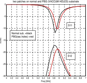
The computed results by using HFSSTMare shown in Fig. 2. It is
observed that for the antennas without the EBG structure resonate at
5.86 GHz with return loss better than−10 dB and for the antennas with
Figure 1. Photo of microstrip antennas with and without the
EBG structure. The substrate thickness is 1.92 mm and its dielectric
constant is 10.2. The antenna size is 6.8 mm×25 mm with a distance
of 48.4 mm. The EBG structure triangular lattice with lattice constant of 1.38 cm and a hole diameter of 1.27 cm.
4 4.2 4.4 4.6 4.8 5 5.2 5.4 5.6 5.8 6 6.2 6.4 6.6 6.8 7 -30
-25 -20 -15 -10 -5
0 two patches on normal and PBG (VACCUM HOLES) substrate
Freq [GHz]
S(
dB)
S11
S12 Normal sub. =black
PBG(vac.holes) =red
Figure 2. Computed results
of microstrip antennas with and without the EBG structure. An 2 dB mutual coupling reduction is observed at the resonant fre-quency.
4 4.2 4.4 4.6 4.8 5 5.2 5.4 5.6 5.8 6 6.2 6.4 6.6 6.8 7 -30
-25 -20 -15 -10 -5 0
comparsion between two patches on uniform and EBG ( hole5.6 ) substrate
Freq [GHz]
S(
d
B
)
S11
S12 uniformsub.=black
EBG( holes5.6)sub.=red
Figure 3. Computed results
the EBG structure of vacuum holes resonate at 5.96 GHz with return
loss little better than −10 dB. The mutual coupling of the antennas
without the EBG structure is −16.8 dB. In comparison, the mutual
coupling of the patches with the EBG structure is only −18.9 dB.
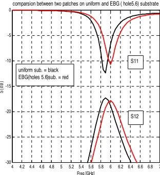
An approximately 2 dB reduction of mutual coupling is achieved. To investigate the effects of a EBG structure as in the previous case is used, but now the hole are filled with a material instead of air with dielectric constant of 5.6.
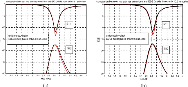
The computed results by using HFSSTMare shown in Fig. 3. It is
observed that for the antennas with the EBG structure of holes (5, 6)
was resonate at 5.92 GHz with return loss better than−10 dB, and the
mutual coupling of the antennas with the EBG structure is −17.8 dB.
An approximately 1 dB reduction of mutual coupling is achieved. Also, to investigate the effects of a EBG structure as in the previous cases are used, but now the hole are filled with a material with dielectric
constant of 10.6. The computed results by using HFSSTM are shown
in Fig. 4. It is observed that for the antenna with the EBG structure of
holes (10.6) resonate at 5.9 GHz with return loss better than−10 dB.
With mutual coupling with the EBG structure is −16.85 dB. We can
compare the computed results between the uniform and EBG substrate (holes of 5.6 and 10.6) in Fig. 5, it is observed that for the antennas with and without the EBG structure of holes have return loss better than
−10 dB. With mutual coupling with the EBG structure is improved by
small values.
4 4.2 4.4 4.6 4.8 5 5.2 5.4 5.6 5.8 6 6.2 6.4 6.6 6.8 7 -30 -25 -20 -15 -10 -5 0
comparsion between two patches on uniform and EBG ( hole10.6) substrate
Freq [GHz] S( d B ) S11 S12 uniformsub.=black EBG( holes10.6)sub.=red
Figure 4. Computed results
of microstrip antennas with and without the EBG structure. An 0.05 dB mutual coupling reduc-tion is observed at the resonant frequency.
4 4.24.4 4.6 4.8 5 5.25.4 5.6 5.8 6 6.26.4 6.6 6.8 7 -30 -25 -20 -15 -10 -5 0
comparsion between two patches on uniform , EBG ( hole5.6)and EBG ( hole10.6) substrate
Freq [GHz] S( d B ) S11 S12 uniformsub.=black EBG( holes10.6)sub.=red EBG(holes5.6)sub.=green
Figure 5. Computed results
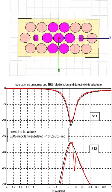
To investigate the effects of a EBG structure as in the previous cases by change only the kind of the material of middle holes of the structure with dielectric constant of 5.6 and 10.6 value, Fig. 6 shows a photograph of the fabricated antennas with the EBG structure. The
computed results by using HFSSTM are shown in Fig. 7 the mutual
coupling between patches with the EBG structure at the resonant frequency is not improved.
Figure 6. Photo of microstrip antennas with the EBG structure.
4 4.2 4.4 4.6 4.8 5 5.2 5.4 5.6 5.8 6 6.2 6.4 6.6 6.8 7 -30
-25 -20 -15 -10 -5 0
comparsion betw een tw o patches on uniform and EBG (middel holes only 5.6 ) substrate
Freq [GHz]
S(
dB)
S11
S12 uniformsub.=black
EBG(middel holes only5.6)sub.=red
(a)
4 4.2 4.4 4.6 4.8 5 5.2 5.4 5.6 5.8 6 6.2 6.4 6.6 6.8 7 -30
-25 -20 -15 -10 -5 0
comparsion between two patches on uniform and EBG (middel holes only 10.6 ) substrate
Freq [GHz]
S(
dB
)
S11
S12 uniformsub.=black
EBG( middel holes only10.6)sub.=red
(b)
Figure 7. Computed results of microstrip antennas with and without
the EBG structure. mutual coupling is not improved at the resonant frequency.
By changing the materials of the holes (porcelain holes with dielectric constant of 5.7 around the patches and vacuum in the middle
holes) as in Fig. 8. The computed results by using HFSSTMare shown
Figure 8. Photo of microstrip antennas with the EBG structure (porcelain holes of 5.7 around the patches and vacuum in the middle holes).
4 4.2 4.4 4.6 4.8 5 5.2 5.4 5.6 5.8 6 6.2 6.4 6.6 6.8 7
-30 -25 -20 -15 -10 -5 0
tw o patches on normal and EBG mid vaccum proclin holes substrate
Freq [GHz]
S(
dB
)
S11
S12 uniform sub. =black
EBG mid vaccum proclin holes =red
Figure 9. Computed results of microstrip antennas with and without
the EBG structure. An 1 dB mutual coupling reduction is observed at the resonant frequency.
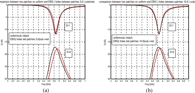
To simplify the EBG structure as in the previous cases by change the structure of holes between the patches with dielectric constant of 5.6 and 10.6 values, Fig. 10 shows a photograph of the fabricated antennas with the EBG structure. The computed results by using
HFSSTM are shown in Fig. 11, the mutual coupling with the EBG
Figure 10. Photo of microstrip antennas with simplify EBG structure.
4 4.2 4.4 4.6 4.8 5 5.2 5.4 5.65.8 6 6.2 6.46.6 6.8 7 -30
-25 -20 -15 -10 -5 0
comparsion between two patches on uniform and EBG ( holes between patches 5.6 ) substrate
Freq [GHz]
S(
d
B
)
S11
S12 uniformsub.=black
EBG( holes bet.patches 5.6)sub.=red
(a)
4 4.2 4.4 4.6 4.8 5 5.2 5.4 5.6 5.8 6 6.26.4 6.6 6.8 7 -30
-25 -20 -15 -10 -5 0
comparsion between two patches on uniform and EBG ( holes between patches 10.6 ) substrat
Freq [GHz]
S(
d
B
)
S11
S12 uniformsub.=black
EBG( holes bet.patches 10.6)sub.=red
(b)
Figure 11. Computed results of microstrip antennas with and without
simplify EBG structure. Mutual coupling is improved by small values at the resonant frequency.
3.2. Large Number of Holes
Two pairs of microstrip antennas are fabricated on Roger RT Duroid 6010 substrates. The permittivity of the substrate is 10.2, and the
substrate thickness is 1.92 mm. The antenna’s size is 6.8 mm×5 mm,
and the distance between the antennas’ edges is 48.4 mm. The antennas
are fabricated on a ground plane of 150 mm×100 mm. Fig. 12 shows
a photograph of the fabricated antennas with and without the EBG
structure. For the EBG structures, triangular lattice with lattice
The computed results by using HFSSTM are shown in Fig. 13. The mutual coupling with the EBG structure is improved by 2 dB at the resonant frequency. Then, to investigate the effects of a EBG structure as in the previous cases are used, but now the holes are filled
Figure 12. Photo of microstrip antennas with and without the
EBG structure. The substrate thickness is 1.92 mm and its dielectric
constant is 10.2. The antenna size is 6.8 mm×25 mm with a distance
of 48.4 mm. The EBG structure triangular lattice with lattice constant of 1.38 cm and a hole diameter of 1.27 cm.
4 4.2 4.4 4.6 4.8 5 5.2 5.4 5.6 5.8 6 6.2 6.4 6.6 6.8 7 -30
-25 -20 -15 -10 -5 0
comparsion between two patches on uniform and EBG ( vaccum holes) substrate
Freq [GHz]
S(
d
B
)
S11
S12 uniform sub. =black
EBG(vac. holes)sub.=red
Figure 13. Computed results
of microstrip antennas with and without simplify EBG structure. An 2 dB mutual coupling reduc-tion is observed at the resonant frequency.
4 4.2 4.4 4.6 4.8 5 5.2 5.4 5.6 5.8 6 6.2 6.4 6.6 6.8 7 -30
-25 -20 -15 -10 -5 0
comparsion between two patches on uniform and EBG ( hole5.6) substrate
Freq [GHz]
S(
d
B
)
S11
S12 uniform sub. = black
EBG(holes 5.6)sub. = red
Figure 14. Computed results
of a material with dielectric constant of 5.6 and 10.6. The computed
results by using HFSSTM are shown in Fig. 14 and Fig. 15.
3.3. Defect Mode
A defect state is created in the forbidden gap where an electromagnetic
mode is allowed and localization of the energy occurs [3]. A
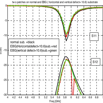
2-DEBG antenna structure is fabricated with a defect point in the EBG substrate, placed under the patch location. This point defect is used to localize the field within the defect region, hence, confining the energy under the patch. The energy confinement leads to a more efficient antenna as well as providing a simpler method of fabrication. For small number of holes to investigate the effects of a EBG structure as in the previous cases are used, but now with defect with dielectric constant of 10.6. Fig. 17 shows Photo of microstrip antennas with horizontal
and vertical defect EBG structure (defect size of 5 mm×8 mm). The
computed results by using HFSSTMare shown in Fig. 18. The presence
of a point defect under the patch, allows a higher concentration of electromagnetic energy density within the cavity formed by the patch and the fact that the antenna leakage can simply be controlled by tuning to or away from a defect resonance line, and can be used
4 4.2 4.4 4.6 4.8 5 5.2 5.4 5.6 5.8 6 6.2 6.4 6.6 6.8 7
-30 -25 -20 -15 -10 -5 0
comparsion between two patches on uniform and EBG ( hole10.6) substrate
Freq [GHz]
S(dB)
S11
S12 uniform sub. =black
EBG(holes10.6)sub. = red
Figure 15. Computed results
of microstrip antennas with and without simplify EBG structure. An 2 dB mutual coupling reduc-tion is observed at the resonant frequency.
4 4.2 4.4 4.6 4.8 5 5.2 5.4 5.6 5.8 6 6.2 6.4 6.6 6.8 7
-30 -25 -20 -15 -10 -5 0
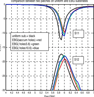
comparsion between two patches on uniform and EBG substrates
Freq [GHz]
S(
dB
)
S11
S12 uniform sub.= black
EBG(vaccum holes) =red EBG( holes5.6) =green EBG( holes10.6) =blue
Figure 16. Computed results
Figure 17. Photo of microstrip antennas with horizontal and vertical
defect EBG structure. The substrate thickness is 1.92 mm and its
dielectric constant is 10.2. The antenna size is 6.8 mm×25 mm with a
distance of 48.4 mm. The EBG structure triangular lattice with lattice
constant of 1.38 cm and a hole diameter of 1.27 cm. Defect size is
5 mm×8 mm.
4 4.2 4.4 4.6 4.8 5 5.2 5.4 5.6 5.8 6 6.2 6.4 6.6 6.8 7 -30
-25 -20 -15 -10 -5 0
tw o patches on normal and EBG ( horizontal and vertical defect= 10.6) substrate
Freq [GHz]
S(dB)
S11
S12 normal sub. =black
EBG(Horizontaldefect=10.6)sub.=red EBG(vertical defect=10.6)sub.=green
Figure 18. Computed results of microstrip antennas with and without
simplify EBG structure. Comparison between normal and EBG
to inhibit or stimulate the coupling between different elements of a microstrip patch antennas array. Also, to investigate the effects of a EBG structure as in the previous cases are used, but now the middle holes are filled with a material with dielectric constant of 10.6. Photo of microstrip antennas with horizontal defect and the computed results
of horizontal defect (size of 5 mm×8 mm) by using HFSSTMare shown
in Fig. 19.
4 4.2 4.4 4.6 4.8 5 5.2 5.4 5.6 5.8 6 6.2 6.4 6.6 6.8 7 -30
-25 -20 -15 -10 -5 0
tw o patches on normal and EBG (Middle holes and defect =10.6) substrate
Freq [GHz]
S(
dB)
normal sub. =black
EBG(middleholes&defect=10.6)sub.=red
S11
S12
Figure 19. Photo of microstrip antennas with horizontal defect
and the Computed results of microstrip antennas with and without simplify defect EBG structure. Comparison between normal and EBG substrates with horizontal defect with dielectric constant of 10.6.
antennas with horizontal and vertical defect EBG structure (defect
size of 5 mm×8 mm). The computed results by using HFSSTM are
shown in Fig. 21.
But by changing the defect with dielectric constant of 5.6, the
computed results by using HFSSTM are shown in Fig. 22.
For microstrip patch antennas array, the excitation frequency is
Figure 20. Photo of microstrip antennas with horizontal and vertical
defect EBG structure. The substrate thickness is 1.92 mm and its
dielectric constant is 10.2. The antenna size is 6.8 mm×25 mm with a
distance of 48.4 mm. The EBG structure triangular lattice with lattice
constant of 1.38 cm and a hole diameter of 1.27 cm. Defect size is
5 mm×8 mm.
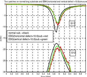
4 4.2 4.4 4.6 4.8 5 5.2 5.4 5.6 5.8 6 6.2 6.4 6.6 6.8 7 -30
-25 -20 -15 -10 -5 0
Tw o patches on normal long substrate and EBM (horizontal and vertical defect =10.6)strucure
Freq [GHz]
S(
dB
)
S11
S12 normal sub. =black
EBG(horizontal defect=10.6)sub.=red EBG(vertical defect=10.6)sub.=green
Figure 21. Computed results
of microstrip antennas with and without simplify EBG structure. Comparison between normal and EBG substrates with horizontal and vertical defect with dielectric constant of 10.6.
4 4.2 4.4 4.64.8 5 5.25.4 5.6 5.8 6 6.2 6.46.6 6.8 7 -30
-25 -20 -15 -10 -5 0
Two patches on normal long substrate and EBM (horizontal and vertical defect =5.6)strucure
Freq [GHz]
S(dB
)
S11
S12 normal sub. =black
EBG(horizontal defect=5.6)sub.=red EBG(vertical defect=5.6)sub.=green
Figure 22. Computed results
tuned to the horizontal defect. On the other hand, since the excitation frequency is away from the vertical resonance, and yet within the stop band of the 2-DEBG substrate. As we increase the dielectric constant of the defect, the mutual coupling will be improved and tuned to the resonance frequency as in Fig. 21.
3.4. Mushroom-like EBG Structure
Two pairs of microstrip antennas are fabricated on Roger RT/Duroid 6010 substrates. The permittivity of the substrate is 10.2, and the
substrate thickness is 1.92 mm. The antenna’s size is 6.8 mm×5 mm,
and the distance between the antennas’ edges is 38.8 mm. The antennas
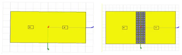
are fabricated on a ground plane of 100 mm×50 mm. Fig. 23 shows
a photograph of the fabricated antennas with and without the EBG structure. For the EBG structures [11], the mushroom-like patch size is 3 mm and the gap between the patches is 0.5 mm. Four columns of mushroom-like patches are inserted between the antennas and was originally designed to have a gap at approximately 5.8 GHz.
Figure 23. Photo of microstrip antennas with and without the
EBG structure. The substrate thickness is 1.92 mm and its dielectric
constant is 10.2. The antenna size is 6.8 mm×5 mm with a distance
of 38.8 mm. The EBG mushroomlike patch (4 coln.) size is 3 mm and the gap width is 0.5 mm.
The computed results by using HFSSTM are shown in Fig. 24. It
is observed that both antennas have return loss better than −10 dB.
For the antennas without the EBG structure, the mutual coupling is
−18.5 dB. In comparison, the mutual coupling of the antennas with
the EBG structure is only −22.5 dB.
4 4.2 4.4 4.6 4.8 5 5.2 5.4 5.6 5.8 6 6.2 6.4 6.6 6.8 7 -30
-25 -20 -15 -10 -5 0
Different no of mushroom patches
Freq [GHz]
S(
dB)
U33 No EBG
--- WithEBG
S12
Figure 24. Computed results of microstrip antennas with and without
the EBG structure. An 4 dB mutual coupling reduction is observed at the resonant frequency.
Figure 25. A photograph of the fabricated antennas with and odd
number of columns of EBG structure (3 coln. and 5 coln.).
structure. The computed results by using HFSSTM are shown in
Fig. 26. It is observed that for the antennas without the EBG structure,
the mutual coupling is −18.5 dB. In comparison, the mutual coupling
of the antennas with the EBG structure (3 coln.) is −19.8 dB while
the EBG structure (5 coln.) only−23.5 dB.
Secondly, we compare the different number of mushroom-like
patch structure for even number of columns. Fig. 27 shows a
photograph of the fabricated antennas with and even number of
columns of EBG structure. The computed results by using HFSSTM
are shown in Fig. 28. It is observed that for the antennas without
4 4.2 4.4 4.6 4.8 5 5.2 5.4 5.6 5.8 6 6.2 6.4 6.6 6.8 7 -30
-25 -20 -15 -10 -5 0
Different no of mushroom patches
Freq [GHz]
S12
(d
B
)
normal=red
3mushroom-patchescoln.=black 5mushroom-patchescoln.=blue
Figure 26. Computed results of microstrip antennas with and
without different EBG structure. An 5 dB mutual coupling reduction is observed at the resonant frequency for 5 coln. of mushroom-like patch structure.
Figure 27. A photograph of the fabricated antennas with and even
the mutual coupling of the antennas with the EBG structure (2 coln.)
is −19.2 dB while the EBG structure (4 coln.) only −22.5 dB and
the EBG structure (6 coln.) only −23.5 dB. From this computed
demonstration, it can be concluded that the EBG structure can be utilized to reduce the antenna mutual coupling between array elements. The reduction of mutual coupling improved by increasing number of columns of mushroom-like patches structure. Fig. 29 demonstrated the effect of different number of columns on the mutual coupling of
microstrip patch antennas array by using HFSSTM.
4 4.2 4.4 4.6 4.8 5 5.2 5.4 5.6 5.8 6 6.2 6.4 6.6 6.8 7 -30 -25 -20 -15 -10 -5 0
Different no of mushroom patches
Freq [GHz] S12 (dB) normal=red 2mushroom-patchescoln.=black 4mushroom-patchescoln.=blue 6mushroom-patchescoln.=brown
Figure 28. Computed results
of microstrip antennas with and without different EBG structure. An 5 dB mutual coupling reduc-tion is observed at the
reso-nant frequency for 6 coln. of
mushroom-like patch structure.
4 4.2 4.4 4.6 4.8 5 5.2 5.4 5.6 5.8 6 6.2 6.4 6.6 6.8 7 -30 -25 -20 -15 -10 -5 0
Different no of mushroom patches
Freq [GHz] S1 2 (d B ) 2mushroom-patches=red 3mushroom-patches=black 4mushroom-patches=blue 5mushroom-patches=brown 6mushroom-patches=green
Figure 29. Computed results of
microstrip antennas with different EBG structure. An 5 dB mutual coupling reduction is observed at the resonant frequency for 6 coln. of mushroom-like patch structure.
4. CONCLUSION
A 2-DEBG structure was integrated with two element of microstrip patch antennas array. The properties of this structure and the effects
of the substrate were studied using a HFSSTM code. It is instructive
show the highest mutual coupling. The small number of holes case and the large number of holes case have some effects on reducing the mutual coupling. A 1.5 dB mutual coupling reduction is noticed for the former case and a 2 dB reduction is observed for the latter case. The presence of the defect under the patch can increase the radiated power due to the energy storage under the antenna and a 3.5 dB mutual coupling reduction is noticed for the defect mode. The lowest mutual coupling is obtained in the mushroom-like patches structure case as a 5 dB reduction is achieved. On the other hand, the mushroom-like patches structure is more expensive than the other approaches. This comparison demonstrates the EBG structure can be utilized to reduce the antenna mutual coupling between array elements and the antenna leakage can simply be controlled by tuning to or away from a defect resonance line, can be used to inhibit or stimulate the coupling between
different elements of microstrip patch antennas array. Therefore,
incorporating point defects in a 2-DEBG substrate for microstrip patch antennas array also present itself as a viable approach in designing more efficient antenna arrays.
REFERENCES
1. Agi, K., K. J., Malloy, E. Schamiloglu, M. Mojahedi, and E. Niver, “Integration of a microstrip patch antenna with a two-dimensional
photonic crystal substrate,” Electromagnetics, Vol. 19, 277–290,
1999.
2. Parker, G. and M. Charlton, “Photonic crystals,” Physics World,
Vol. 13, 29–34, Aug. 2000.
3. Joannopoulos, J. D., R. D. Meade, and J. Winn, Photonic
Crystals: Molding the Flow of Light, Princeton University Press, Princeton, N.J., 1995.
4. Yang, F. and Y. Rahmat-Samii, “Step-like structure and EBG structure to improve the performance of patch antennas on high
dielectric substrate,”Proc. IEEE AP-S Dig., Vol. 2, 482–485, July
2001.
5. Gonzalo, R., P. Maagt, and M. Sorolla, “Enhanced patch-antenna performance by suppressing surface waves using photonic-bandgap
substrates,”IEEE Trans. Microwave Theory Tech., Vol. 47, 2131–
2138, Nov. 1999.
6. Radisic, V., Y. X. Qian, R. Coccioli, and T. Itoh, “Novel 2-D
photonic bandgap structure for microstrip lines,”IEEE Microwave
and Guided Wave Letters, Vol. 8, 69–71, 1998.
structures used as filters in microstrip circuits,”IEEE Microwave and Guided Wave Letters, Vol. 8, 336–338, 1998.
8. Agi, K., L. D. Moreland, E. Schamiloglu, M. Mojahedi,
K. J. Malloy, and E. R. Brown, “Photonic crystals: A
new quasi-optical component for high-power microwaves,” IEEE
Transactions on Plasma Science, Vol. 24, 1067–1071, 1996. 9. Yang, H. Y. D., N. G. Alexopoulos, and E. Yablonovitch,
“Photonic band-gap materials for high-gain printed circuit
antennas,” IEEE Transactions on Antennas and Propagation,
Vol. 45, 185–187, 1997.
10. Sievenpiper, D., L. Zhang, R. F. J. Broas, N. G. Alexopolus, and E. Yablonovitch, “High-impedance electromagnetic surfaces with
a forbidden frequency band,” IEEE Trans. Microwave Theory
Tech., Vol. 47, 2059–2074, Nov. 1999.
11. Yang, F. and Y. Rahmat Sami, “The effects of an electromagnetic bandgap (EBG) structure on two element microstrip patch
antenna array,” IEEE Transactions Antennas and Propagation,
Vol. 51, No. 10, 2936–2946, Oct. 2003.
12. Sievenpiper, D. F., “High-impedance electromagnetic surfaces,” Ph.D. dissertation, UCLA, 1999.
13. Chang, C., Y. Qian, and T. Itoh, “Analysis and applications
of uniplanar compact photonic bandgap structures,” Progress In
Electromagnetic Research, PIER 41, 211–235, 2003.
14. Xu, H. J., Y. H. Zhang, and Y. Fan, “Analysis of the
con-nection between K connector and microstrip with
electromag-netic bandgap (EBC) structures,” Progress In Electromagnetic
Research, PIER 73, 239–247, 2007.
15. Pirhadi, A., M. Hakkak, and F. Keshmiri, “Using electromagnetic bandgap superstrate to enhance the bandwidth of probe FED
microstrip antenna,” Progress In Electromagnetic Research,