A Coupled-Line Based L-Section DC-Isolated Dual-Band Real
to Real Impedance Transformer and Its Application
to a Dual-Band T-Junction Power Divider
Mohammad A. Maktoomi1, * and Mohammad S. Hashmi1, 2
Abstract—This paper presents a dual-band impedance transformer for real source and load impedances that is capable of providing matching at two arbitrary frequencies. There are two possible configurations of the proposed technique, and both the configurations are simple and possess flexibility to cater to wide range of impedance environments. A very useful feature of the design is its inherent ability to provide DC isolation. A prototype, which works at 1 GHz and 2 GHz, fabricated using Roger’s RO4350B laminate validates the proposed design with a good match between theoretical and experimental results. In addition, a dual-band T-junction power divider is reported to demonstrate the usefulness of the proposed impedance transformer.
1. INTRODUCTION
Impedance transformers are present in diverse RF and microwave applications irrespective of whether the applications are single-band or multi-band. Impedance transformer operating at two/multi-frequencies finds applications in the design of dual-band/multi-band amplifiers, oscillators, mixers, power splitter/combiners, antennas etc. [1–4]. Three types of matching networks are of interest to the circuit designers:
1. Real impedance to real impedance transformer. 2. Complex impedance to real impedance transformer. 3. Complex impedance to complex impedance transformer.
For example, a real to real impedance transformer is useful in power dividers [5], a complex to real impedance transformer useful in amplifiers [4], and a complex to complex impedance transformer useful in multi-stage amplifiers for inter-stage matching [6].
There have been numerous reports of dual-band matching techniques that cater to the scenarios mentioned above. For example, a transformer for providing match at a frequency and its first harmonic was reported in [7], Monzon proposed a small dual-frequency transformer to match real source and load impedances [8], whereas Chebyshev impedance transformer reported in [9, 10] and Pi-section transformer [11] also match real load impedance to real source impedance at two distinct frequencies. Furthermore, there could be a situation when the load impedance is complex as well as frequency-dependent, for instance, the input impedance of transistor while looking into its gate terminal. The design techniques reported in [12–22] pretty much address this scenario but with some limitations. For example, the technique reported in [12] provides matching between complex loads and real source impedances but does not consider frequency-dependent load. Furthermore, a three section
Received 5 November 2014, Accepted 29 November 2014, Scheduled 10 December 2014 * Corresponding author: Mohammad A. Maktoomi ([email protected]).
1 Wireless Systems Lab, Department of Electronics and Communications Engineering, IIIT Delhi, New Delhi 110020, India.2iRadio
transformer and later a generalized impedance transformer were respectively reported in [14, 15], but both of these techniques possess very complex design equations. Dual-band transformers using stub-loaded transmission line [16], T-section network [17], and dual-band line with different characteristic impedances [18] find utility in dual-band power amplifier design. A lumped components based dual-band impedance transformers was also reported [22], but it had inherent weaknesses as the operating frequency increased [6]. Recently, coupled lines have been utilized in matching complex load impedances to real source impedance [19–21, 23]. Lastly, very few tri-band/quad-band real to real impedance transformers have also been reported [24, 25].
This paper, for the first time, proposes a real to real impedance transformer capable of operating at two distinct frequencies concurrently with an inherent DC block feature. The proposed design, consisting of two sections, have been analysed to obtain closed form equations which is then simulated, fabricated, and experimentally verified. Subsequently, the usefulness of the proposed impedance transformer is demonstrated through a new dual-band T-junction power divider.
2. PROPOSED IMPEDANCE TRANSFORMER
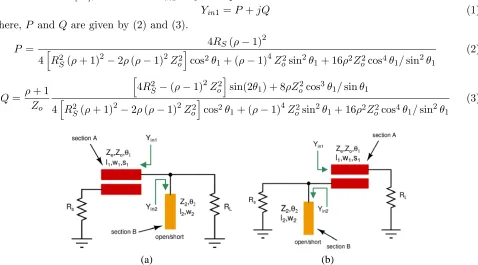
The two proposed configurations are depicted in Figure 1. It can be seen that the only difference between these configurations is in the placement of stub. The design with stub on the load side is named as configuration-I, whereas the design with stub on the source side is named as configuration-II. The analysis of both these configurations is given in subsequent subsections.
2.1. Analysis of Configuration-I
The configuration-I is shown in Figure 1(a). It is apparent that it consists of a parallel coupled line (Section A), and a short or an open stub (Section B). In Section A, Ze is the even-mode impedance,
Zo the odd-mode impedance, and θ1 the electrical length of the coupled line whereas Z2 and θ2 are
the characteristic impedance and electrical length of the stub. Yin1 denotes the admittance looking
into Section A whileYin2 is the admittance looking into Section B. The physical dimensionsl (length), w (width) and s (separation between coupled lines) of respective transmission-line segments are also shown in the figure. All electrical lengths are defined at the first frequency,f1.
As shown in [23], the value ofYin1 may be expressed as follows:
Yin1 =P+jQ (1)
where, P and Qare given by (2) and (3).
P = 4RS(ρ−1)
2
4
R2
S(ρ+ 1)2−2ρ(ρ−1)2Zo2
cos2θ
1+ (ρ−1)4Zo2sin2θ1+ 16ρ2Zo2cos4θ1/sin2θ1
(2)
Q= ρ+ 1
Zo
4R2S−(ρ−1)2Zo2
sin(2θ1) + 8ρZo2cos3θ1/sinθ1
4
R2
S(ρ+ 1)2−2ρ(ρ−1)2Zo2
cos2θ
1+ (ρ−1)4Zo2sin2θ1+ 16ρ2Zo2cos4θ1/sin2θ1
(3)
(a) (b)
The factor ρ in the above expressions is the ratio, Ze/Zo. Equations (2) and (3) reveal that since there are only even powers of sinθ1 and cosθ1, the values of P will remain the same if θ1 is replaced
by π−θ1. Furthermore, the value of Qwill change sign ifθ1 is replaced byπ−θ1 considering that the
denominator of Q contains even powers of sinusoids and that numerator has either odd-powers or 2θ1
terms. With these observations, it can be concluded thatYin1|f1 =Yin∗1|f2 if the value ofθ1 is given by:
θ1 =
(1 +q)π
1 +r (4)
where, q is an integer andr the band-ratio,f2/f1.
Thus, if Yin1|f1 =P+jQ, then Yin1|f2 =P−jQ and vice-versa. Section A is designed in such a manner that:
P = 1/RL (5)
The imaginary part of Yin1 (which is +Q@f1 and −Q@f2) is cancelled by a dual-band susceptance
(Section B) having the following property:
Yin2|f1 =−jQ (6a)
Yin2|f2 = +jQ (6b)
If an open stub is to be used as a dual-band susceptance, the following equations should hold true:
−jQ=j(1/Z2) tanθ2 (7a)
+jQ=j(1/Z2) tan (rθ2) (7b)
Simplification of (7) yields,
θ2=
(1 +s)π
1 +r , where sis an Integer (8a)
Z2=−tanθ2/Q (8b)
Similarly, for short stub to work as a dual-band susceptance, the following equations need to be satisfied:
−jQ=−j(1/Z2) cotθ2 (9a)
+jQ=−j(1/Z2) cot(rθ2) (9b)
Further simplification of (9) results into:
θ2=
(1 +s)π
1 +r , where sis an Integer (10a)
Z2= cotθ2/Q (10b)
2.2. Analysis of Configuration-II
Analysis of this configuration is similar to the previous one with the exception of the following changes. 1. RS in Equations (2) and (3) needs to be replaced byRL.
2. The coupled line is now designed such that
P = 1/RS (11)
3. DESIGN PROCEDURE
Design steps for the proposed network are as follows:
1. For given values ofr, RL and RS, and assuming an appropriate value ofZo (say, 25 Ω), the value ofρ is calculated with the help of (2), (4) and (5). A realizable value ofρ lies anywhere between 2 and 4 [25]. Alternatively, assuming a suitable value forρ, the value ofZo can be determined using the same equations. It is reiterated that P = 1/RL orP = 1/RS needs to be set depending upon whether the configuration-I or the configuration-II is used. Thus, the corresponding value ofZe is
ρ∗Zo. If the obtained parameters for Section A are not physically realizable, then one needs to
2. Subsequently, the value of Q is evaluated with the help of (3), and using the design procedure of dual-band stubs as described previously, a suitable Section B may be designed. Practically, θ2 is
either greater or less than 90◦. It is to be noticed that the value of integer s depends on the sign ofQ. There are four possible cases:
(a) The value of Q is positive/negative and open/short stub is to be used in Section B: it follows from (8b)/(10b) that tanθ2/cotθ2 must be negative to ensure a positive value of Z2. This
implies that the integer s must be chosen such that θ2 comes out to be greater than 90◦ in
(8a)/(10a).
(b) The value ofQ is positive/negative, and short/open stub is to be used in Section B: it follows from (10b)/(8b) that cotθ2/tanθ2 must be positive as well to ensure a positive value of Z2.
This implies that the integer smust be chosen such that θ2 comes out to be less than 90◦ in
(10a)/(8a).
Furthermore, the requirement to obtain physically realizable design parameters for stubs also affects the choice of integers. Lastly, if using open stub as Section B does not yield a physically realizable
l2 and w2, then one will try a short stub and vice versa.
A design example shall make the procedure more clear. To that end, suppose that RL = 100 Ω is to be matched to RS = 50 Ω at f1 = 1 GHz and f2 = 2 GHz which implies r = 2, and thus θ1 = 60◦ from (4) considering q = 0 for compact size. Furthermore, a value of Zo = 25 Ω is
assumed. Since P = 0.01 mho from (5), the value of ρ is found from (2) which comes out to be 2.1332, omitting unreasonable values. The value ofQ corresponding to ρ = 2.1332 is found to be 0.04639 mho from (3). Next, since the value ofQis positive,sis set as 1 in 8(a) so that θ2= 120◦
and tanθ2 becomes negative which ensures a positive value of Z2. The value of Z2 evaluates to
37.34 Ω from (8b). This completes the design.
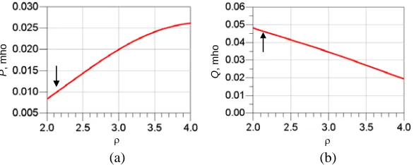
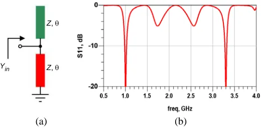
Although Equation (5) along with (2) and (4) can be solved by algebraic means, a plot such as that shown in Figure 2 is very useful for a quick estimate ofρ and Q and for the intuition it may provide. For example, the question whether we can obtain a match if RL = 20 Ω in the above example can be quickly and easily answered with the help of Figure 2(a) which clearly shows that it is not possible as the plot does not reachP = 1/RL= 0.05 mho.
4. RESULTS AND DISCUSSIONS
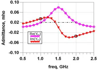
As a very first simulation example, it is shown that Yin1 is complex conjugate at the two frequencies,
ifθ1 is given by (4). To that end, a coupled line withZe = 75 Ω and Zo = 25 Ω is considered. Design
frequencies are assumed to bef1= 1 GHz andf2 = 2 GHz as an example, which corresponds toθ1= 60◦.
A plot ofYin1 forRS = 50 Ω is shown in Figure 3. It can be readily observed that the real part is same
at the two frequencies (please see the dotted line), and the imaginary part just changes its sign as the frequency goes from f1 to f2 (please see the two circles).
P
, mho
Q
, mho
ρ ρ
(a) (b)
Figure 2. Variation ofP andQ(@f1) withρ in the above example. (a) Plot ofP: arrow indicates the
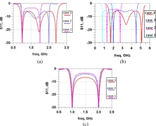
A series of simulation is done to show the flexibility of the proposed circuits in matching different load and source impedances. It is assumed that during all these simulations the source side impedance (RS) is 50 Ω.
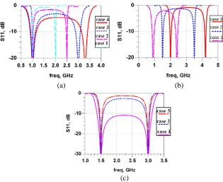
First, as shown in Table 1, the configuration-I is considered, and the load andf1are kept fixed while
the value of f2 is varied. OC denotes the use of an open circuit stub as Section B, whereas SC denotes
the use of a short circuit stub. It is noticed form Table 1 that one cannot go beyond f2 = 3.3 GHz
as the value of required ρ will be greater than 4 which may pose challenges during fabrication. The corresponding return loss plots are shown in Figure 4(a).
In Table 2, the design parameters are shown for the case where the load is again fixed, but nowf1
and f2 are both chosen arbitrarily. Figure 4(b) shows the return loss for this case.
Lastly, in Table 3, f1 and f2 are both held at fixed valuef1 = 1.5 GHz andf2 = 3 GHz while the
load impedance is swept. A good matching can be observed from return loss plots which appear in Figure 4(c). Again, it may be observed from Table 3 that as the value of the load impedance increases from 40 Ω to 80 Ω, the required value ofZedecreases, and ultimately a situation will come (RL= 100 Ω, for example) where the requiredρ will be lesser than 2.
Re(Y )in1
Im(Y )in1
Figure 3. Variation of the real and imaginary parts ofYin1. Re(·) returns the real part of a complex number whereas Im(·) returns the imaginary part.
Table 1. Configuration-I, f1= 1 GHz,Zo= 25 Ω,RL= 100 Ω.
Cases f2 (GHz) Ze (Ω) θ1 (deg) Z2 (Ω) θ2 (deg)
1 2 53.33 60 37.34 120, OC
2 2.5 68.36 51.43 145.19 102.86, OC
3 3 85.36 45 44.334 45, SC
4 3.3 97.05 41.86 56.52 41.86, SC
Table 2. Configuration-I, Zo= 25 Ω,RL= 100 Ω.
Cases f1 (GHz) f2 (GHz) Ze (Ω) θ1 (deg) Z2 (Ω) θ2 (deg)
1 0.9 2.4 73.74 49.10 32.01 49.10, SC
2 1.5 3.5 63.20 54 90.15 108, OC
3 2 4.2 56.24 58.06 48.67 116.13, OC
Table 3. Configuration-I, f1= 1.5 GHz, f2= 3 GHz, Zo= 25 Ω.
Cases RL (Ω) Ze (Ω) θ1 (deg) Z2 (Ω) θ2 (deg)
case 3
case 2
case 1
(a) (b)
(c)
Figure 4. Return loss for the designs of (a) Table 1, (b) Table 2, (c) Table 3.
Table 4. Configuration-II,f1 = 1 GHz,Zo = 25 Ω,RL= 20 Ω.
Cases f2 (GHz) Ze (Ω) θ1 (deg) Z2 (Ω) θ2 (deg)
1 2 53.11 60 31.37 120, OC
2 2.5 73.28 51.43 108.51 102.86, OC 3 2.9 93.61 46.15 27.60 46.15, SC
Table 5. Configuration-II,Zo = 25 Ω,RL= 20 Ω.
Cases f1 (GHz) f2 (GHz) Ze (Ω) θ1 (deg) Z2 (Ω) θ2 (deg)
1 0.8 1.8 62.50 55.38 57.17 110.76, OC 2 1.3 2.75 57.28 57.78 41.45 115.56, OC 3 2 4.5 62.50 55.38 57.17 110.77, OC
4 1.7 5.1 99.3 45 29.56 45, SC
Table 6. Configuration-II,f1 = 1 GHz,f2 = 2 GHz, Zo= 25 Ω.
Cases RL (Ω) Ze (Ω) θ1 (deg) Z2 (Ω) θ2 (deg)
1 30 58.69 60 36.80 120, OC 2 45 70.27 60 46.13 120, OC 3 65 93.86 60 67.84 120, OC
case 3
case 2
case 1
case 3
case 2
case 1
(a) (b)
(c)
Figure 5. Return loss for the designs of (a) Table 4, (b) Table 5, (c) Table 6.
Section A
Section B 50 Ω line
(a) (b)
Figure 6. (a) The manufactured prototype in our lab. This is a configuration-I type matching network. (b) The measurement result as compared to the EM-simulation result.
A prototype to work atf1 = 1 GHz andf2= 2 GHz is implemented for configuration-I using Roger’s
RO4350B laminate on 1oz copper cladding to show the practical utility of the proposed design. The load is a 20.5 Ω CRCW series SMD resistor available from Vishay. The prototype is shown in Figure 6(a) where the physical dimensions (in mm) are as follows: l1 = 31.620,w1 = 1.750,s1 = 0.285, l2 = 59.517
and w2= 1.112. The corresponding simulation and measurement results are shown in Figure 6(b).
Next, to show the practical utility of configuration-II, a T-junction power divider shown in Figure 7(a) is considered [5]. Its equivalent circuit looking from port 1 is shown in Figure 7(b). Since to have equal power division, the paths from port 1 to port 2 and from port 1 to port 3 are the same, the coupled line impedances as well as the impedance of the right-side termination gets halved in Figure 7(b). The equivalent circuit may readily be recognized as the proposed configuration-II, where the requirement is to matchRL=Z0/2 to RS =Z0, where Z0(= 50 Ω) is the port impedance.
Based on this idea, a dual-band T-junction power divider is designed and implemented to work at
f1 = 1 GHz andf2= 2.1 GHz. The prototype and correspondingS-parameters are depicted in Figure 8.
(a) (b)
Figure 7. (a) A dual-band T-junction power divider. (b) Equivalent circuit of the divider looking into the port 1.
Simulated
Measured
Simulated S21
Simulated S 31 Measured S 21
Measured S 31 72.2 mm
45.1 mm
(a) (b) (c)
Figure 8. (a) Photograph of the designed T-junction divider. (b) Simulated/measured Return loss of port 1. (c) Simulated/measured transmissions.
Z, θ
Z, θ
Yin
(a) (b)
Figure 9. (a) A dual-band complex impedance using parallel combinations of open and short stubs to fine-tune out-of-the-band performance. (b) Simulated Return loss for the case4 of Table 1 showing better out-of-the-band performance.
use a parallel combination of a short and open stub shown in Figure 9(a), instead of using only either of them.
It may be proved in a manner similar to the one discussed in Section 2.1 that the value of Z is given by
Z = 1−tan
2θ
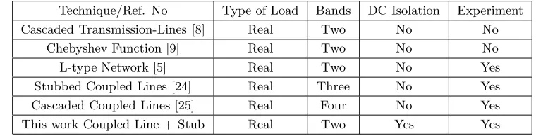
Table 7. Comparision with some existing designs.
Technique/Ref. No Type of Load Bands DC Isolation Experiment
Cascaded Transmission-Lines [8] Real Two No No
Chebyshev Function [9] Real Two No No
L-type Network [5] Real Two No Yes
Stubbed Coupled Lines [24] Real Three No Yes
Cascaded Coupled Lines [25] Real Four No Yes
This work Coupled Line + Stub Real Two Yes Yes
where, θhas the same expression as that of θ2.
Using this parallel stub, case 4 of Table 1 is redesigned to illustrate the improvement; the values of
Z and θ are found to be 34.56 Ω and 125.58◦, respectively. The simulated return loss is depicted in Figure 9(b). It is evident that the out-of-the-band performance is much better than previous result shown in Figure 4(a)/case 4. This solution would however, come at a price of increased layout complexity.
A comparison of the proposed matching network with some popular previously reported designs for real load and source impedances is presented in Table 7.
5. CONCLUSION
A dual-band impedance matching network having two possible configurations, with inherent dc blocking property, have been demonstrated. The effectiveness and flexibility of the proposed configurations have been shown through a number of simulation results. A prototype has been built to validate the performance obtained from the proposed technique. A dual-band T-junction power divider has been proposed as an example application of the developed impedance transformer.
REFERENCES
1. Rawat, K., M. S. Hashmi, and F. M. Ghannouchi, “Dual-band RF circuits and components for multi-standard software defined radios,” IEEE Circuits & Systems Magazine, Vol. 12, No. 1, 12– 32, First Quater 2012.
2. Hashemi, H. and A. Hajimiri, “Concurrent multiband low-noise amplifiers — Theory, design, and applications,” IEEE Transactions on Microwave Theory and Techniques, Vol. 50, No. 1, 288–301, Jan. 2002.
3. Nallam, N. and S. Chatterjee, “Multi-band frequency transformations, matching networks and amplifiers,” IEEE Transactions on Circuits & Systems I: Reg. Papers, Vol. 60, No. 6, 1635–1647, Jun. 2013.
4. Iyer, B. and N. P. Pathak, “A concurrent dual-band LNA for noninvasive vital sign detection system,” Wiley Microwave &Optical Technology Letters, Vol. 56, No. 2, 391–394, Feb. 2014. 5. Park, M. J. and B. Lee, “Dual band design of single stub impedance matching networks with
application to dual band stubbed T junctions,” Wiley Microwave & Optical Technology Letters, Vol. 52, No. 6, 1359–1362, 2010.
6. Hsieh, K.-A., H.-S. Wu, K.-H. Tsai, and C.-K. C. Tzuang, “A dual-band 10/24-GHz amplifier design incorporating dual-frequency complex load matching,” IEEE Transactions on Microwave Theory and Techniques, Vol. 60, No. 6, 1649–1657, Jun. 2012.
7. Chow, Y. L. and K. L. Wan, “A transformer of one-third wavelength in two sections — For a frequency and its first harmonic,” IEEE Microwave and Wireless Components Letters, Vol. 12, No. 1, 22–23, Jan. 2002.
8. Monzon, C., “A small dual-frequency transformer in two sections,” IEEE Transactions on Microwave Theory and Techniques, Vol. 51, No. 4, 1157–1161, Apr. 2003.
10. Castaldi, G., “An exact synthesis method for dual-band Chebyshev impedance transformers,” Progress In Electromagnetics Research, Vol. 86, 305–319, 2008.
11. Wu, Y., Y. Liu, and S. Li, “A compact Pi-structure dual band transformer,” Progress In Electromagnetics Research, Vol. 88, 121–134, 2008.
12. Wu, Y., Y. Liu, and S. Li, “A dual-frequency transformer for complex impedances with two unequal sections,” IEEE Microwave and Wireless Components Letters, Vol. 19, No. 2, 77–79, Feb. 2009. 13. Giannini, F. and L. Scucchia, “A complete class of harmonic matching networks: Synthesis and
application,” IEEE Transactions on Microwave Theory and Techniques, Vol. 57, No. 3, 612–619, Mar. 2009.
14. Liu, X., Y. Liu, S. Li, F. Wu, and Y. Wu, “A three-section dual-band transformer for frequency-dependent complex load impedance,” IEEE Microwave and Wireless Components Letters, Vol. 19, No. 10, 611–613, Oct. 2009.
15. Wu, Y., Y. Liu, S. Li, C. Yu, and X. Liu, “A generalized dual-frequency transformer for two arbitrary complex frequency-dependent impedances,”IEEE Microwave and Wireless Components Letters, Vol. 19, No. 12, 792–794, Dec. 2009.
16. Chuang, M.-L., “Dual-band impedance transformer using two-section shunt stubs,” IEEE Transactions on Microwave Theory and Techniques, Vol. 58, No. 5, 1257–1263, May 2010.
17. Nikravan, M. A. and Z. Atlasbaf, “T-section dual-band impedance transformer for frequency-dependent complex impedance loads,”Electronics Letters, Vol. 47, No. 9, 551–553, Apr. 28, 2011. 18. Rawat, K. and F. M. Ghannouchi, “Dual-band matching technique based on dual-characteristic impedance transformers for dual-band power amplifiers design,” IET Microwaves, Antennas & Propagation, Vol. 5, No. 14, 1720–1729, Nov. 18, 2011.
19. Wu, Y., W. Sun, S.-W. Leung, Y. Diao, and K.-H. Chan, “A novel compact dual-frequency coupled-line transformer with simple analytical design equations for frequency-dependent complex load impedance,”Progress In Electromagnetics Research, Vol. 134, 47–62, 2013.
20. Li, S., B. Tang, Y. Liu, S. Li, C. Yu, and Y. Wu, “Miniaturized dual-band matching technique based on coupled-line transformer for dual-band power amplifiers design,” Progress In Electromagnetics Research, Vol. 131, 195–210, 2012.
21. Wu, Y., Y. Liu, S. Li, and C. Yu, “New coupled-line dual-band dc-block transformer for arbitrary complex frequency-dependent load impedance,” Wiley Microwave & Optical Technology Letters, Vol. 54, No. 1, 139–142, Jan. 2012.
22. Moon, B.-T. and N.-H. Myung, “A dual-band impedance transforming technique with lumped elements for frequency-dependent complex loads,”Progress In Electromagnetics Research, Vol. 136, 123–139, 2013.
23. Maktoomi, M. A., M. S. Hashmi, and F. M. Ghannouchi, “A T-section dual-band matching network for frequency-dependent complex loads incorporating coupled line with DC-block property suitable for dual-band transistor amplifiers,”Progress In Electromagnetics Research C, Vol. 54, 75–84, 2014. 24. Wang, X. H., L. Zhang, Y. Xu, Y. F. Bai, C. Liu, and X.-W. Shi, “A tri-band impedance transformer
using stubbed coupling line,”Progress In Electromagnetics Research, Vol. 141, 33–45, 2013. 25. Bai, Y.-F., X.-H. Wang, C.-J. Gao, Q.-L. Huang, and X.-W. Shi, “Design of compact