ELECTRONICALLY TUNABLE SIGNAL
PROCESSING CIRCUIT
Dinesh Singh
1, Devesh Singh
21,2
Department of Electronics & Communication, AKG, Engineering College, Ghaziabad (India)
ABSTRACT
This paper presents a voltage mode universal filter using two multi-output operational transconductance amplifier (OTA). Proposed multi-input single output universal filter employs two capacitors only and realizes all the standard second order filtering functions from same configuration. Filter parameters namely pole frequency and quality factor can be tuned independently without affecting each other. Performance of proposed filter is verified by Tanner EDA tool at 180nm technology.
Keywords- Operational Transconductance Amplifier (OTA), Universal filter.
I. INTRODUCTION
In analog signal processing, active filter play a vital function in electronic circuit. It has wide area of application
such as in communication, measurement, instrumentation, control systems and biomedical applications. Design
of universal filter has gained considerable attention these days because of its ability to realize all the filter
function from same configuration.
A challenging issue with the continuous time analog filter is RC time constant variation, which decides the filter
parameters. Time constant of circuit varies with processing tolerance, humidity, environmental effects due to the
drift in temperature and aging of components. This problem can be rectified with the tunability feature in the
filter circuit. Thus, the interest is growing in designing of electronically tunable filters which can compensate
the unwanted variation of RC time constant.
The progress of analog technology has grown many filters using various active elements such as operational
transconductance amplifier (OTA), second generation current conveyor (CCII), current differentiation
transconductance amplifier (CDTA), voltage differencing transconductance amplifier (VDTA), Current
controlled conveyor differencing transconductance amplifier (CCCDTA), voltage differencing inverting
buffered amplifier (VDIBA), Voltage differencing differential input buffered amplifier (VD-DIBA), voltage
differencing buffered amplifier (VDBA) etc. These analog blocks are widely used because of their higher
frequency operation, wide dynamic range, and current mode (CM) operation, high bandwidth and low power
consumption.
Some of the active building blocks such as OTA, VDIBA, VDTA are providing more flexibility in analog
circuit designing. These blocks offers tunability feature through their transconductance parameter and also
attention has been given in realization of tunable filters utilizing different active element. But, these reported
circuits lack one or more of the following important features:
(1) Incapable of realizing all the five filter functions namely Low pass (LP), High Pass (HP), Band Pass
(BP), Band Reject (BR), All Pass (AP) [1,2,3,5].
(2) Independent control of filter parameters.[4]
(3) Lesser sensitivity figures.[1,4]
(4) Cascadability [1]
The aim of this paper is to incorporate all these features in a single filter configuration. The proposed
multi-input VM universal filter circuit consists of two OTA, one grounded and one conditionally grounded (for few
filter functions) capacitor. It can realize all the filter functions by proper selection of input voltage levels. Filter
parameters namely quality factor (Q) and pole frequency (ω0) can be tuned independently. Simulation results
using 180nm CMOS parameters are presented to to verify its performance.
The paper is organized as follows. Start with the introduction, section II briefly describes the active element
OTA. Section III describes the realization of proposed universal filter. Section IV presents the simulation result
of proposed filter Section V provides a comparison for proposed filter with available configurations. Finally,
section VI holds the conclusion for the same.
II. OPERATIONAL TRANSCONDUCTANCE AMPLIFIER
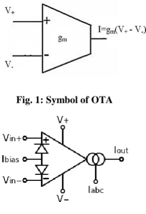
Operational transconductance amplifier (OTA) is basically a voltage controlled current source (VCCS) device.
It generates an output current by processing the input voltage differentially. The circuit symbol and schematic
diagram is shown in Fig.1 and Fig.2 respectively. In this configuration V+ and V- are the high impedence
differential (voltage) input ports and output port is high impedance port yielding the current variable.
Fig. 1: Symbol of OTA
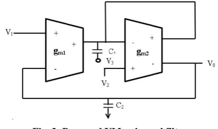
Fig. 2: Schematic diagram of OTA
Where is the input voltage at the non-inverting terminal, is the input voltage at the inverting
terminal and is the transconductance of the amplifier.
The amplifier's output voltage is determined by its output current and associated load as
Thus, the voltage of OTA can be obtained as
The transconductance ( ) parameters of OTA is controlled with the help of an input bias current ( ) shown
in Fig. 2. The transconductance of the amplifier is directly proportional to the bias current. This feature makes it
useful for electronic control of amplifier’s gain.
III. PROPOSED UNIVERSAL FILTER
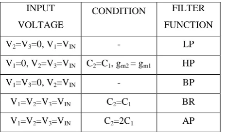
The proposed filter consist of two OTA block (one single output and one dual output) and two capacitors only. it
is shown in Fig. 3.
Fig. 3: Proposed VM universal filter
Output function of proposed universal filter is given as
Second OTA block of proposed filter is required to have both inverting and non inverting output ports.
Required current inversion is obtained by employing a current mirror circuit consisting of transistors M11-M14 in
OTA of [6]. Final transistor level schematic of dual output OTA is shown in Fig. 4. (1)
(2)
(3)
Fig. 4: Dual output OTA
From Eqn. 3, it is clear that all filter function can be realized with the same filter configuration without any
change in the filter circuit which can be seen in table 1.
Table I: Input set for different filter functions
INPUT
VOLTAGE
CONDITION FILTER
FUNCTION
V2=V3=0, V1=VIN - LP
V1=0, V2=V3=VIN C2=C1, gm2 = gm1 HP
V1=V3=0, V2=VIN - BP
V1=V2=V3=VIN C2=C1 BR
V1=V2=V3=VIN C2=2C1 AP
Bandwidth, pole frequency (ω0) and quality factor (Q) can be expressed from the Eqn. 3 in Eqn. (a), (b) and
(c) respectively.
It can be seen from (4) that the pole frequency ( and Q- factor can be tuned independently by equally
varying transconductance and/or capacitances i.e , and
Sensitivity of pole frequency ( and Q-factor is given below: (4a)
(4c) (4b)
From Eqn. 5 it is clear that sensitivity of the proposed filter parameters with respect various active and
passive element is always less than 1. So, it has less unwanted variation.
IV. SIMULATION RESULTS
Theoretical analysis of proposed filter is verified by simulating it on Tanner EDA tool using 180nm CMOS
parameters. Supply voltage is set to 3V. Transistor dimension is given in Table II.
Table II: aspect ratio
M1-M2 W=7µm, L=0.7µm
M3-M7, M11 and M12 W=2.8µm, L=0.7µm
M8-M10, M13 and M14 W=5.6µm, L=0.7µm
The passive components C1 and C2 taken in accordance with the filter response requirement as given in Table I.
The value of the capacitor C1 and C2 both are taken as 5pF. Tuning mechanism is depicted by varying the bias
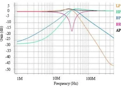
current (which varies its transconductance). Fig. 5,6 and 7 shows the simulated filter responses of LP, HP, BP,
BR and AP at different values of bias current IS.
At IS=100µA, the frequency of the circuit is 16.12MHz.
Fig. 5: Frequency response at Is=100µA
At IS=200µA, the frequency of the circuit is 20.93MHz
.
Fig. 6: Frequency response at Is=200µA
At IS=1.2mA, the frequency of the circuit is 34.43MHz.
Fig. 7: Frequency response at Is=1.2mA
From Fig 5, 6 and 7 it is clearly seen that the pole frequency of the filter increases with increase in the bias
current.
Table III: Comparative study of universal Filters
V. COMPARISION
The proposed filter has been compared with a few existing filter in Table III on the basis of following important
features such as (1) Independently tuned filter parameters (2) Cascadability (3) Component Matching constraints
(4) No of resistors (Grounded/ floating) (5) No of capacitors (Grounded/ floating) (6) No of filter functions –
Low pass, High pass, Band pass, Band stop, All pass (7) Mode of operation (CM/VM) (8) Number of active
elements with name. The total power dissipation of the proposed biquad filter is approximately 1.212mW. It can
be seen from Table III that the proposed filter provides more number of features compared to the reported
filters.
VI. CONCLUSION
Paper proposes a VM universal filter using two OTAs, two capacitors only. It generates all five filter function
without any change in the topology. It has also independently controlled parameters. Tunablity is depicted by
varying the bias current (IS). it consumes 1.212mW at 3Vsupply voltage. Moreover, the configuration requires
component matching constraints in some filter functions i.e (HP), (BR) and (AP). It has low active and passive
sensitivities. All the analysis is performed on Tanner EDA tool at 180nm technology. Features/
References
1 2 3 4 5 6 7 8
[1] Y N Y 0/0 2/0 2 CM 4(OTA)
[2] Y Y N 3/1 2/0 4 VM 2(CC),1(OTA)
[3] Y Y N 1/1 1/0 2 TAM 1(OA)
[4] N Y N 0/0 2/0 5 TAM 5(OTA)
[5] Y Y N 0/0 2/0 3 CM/VM 4(OTA)
REFERENCES
[1] Ali Kircay, Selim Borekci, 2016, “Electronically-Tunable Current-Mode Biquad Design Using
MO-OTAs” Journal of Circuits, Systems, and Computers, Vol. 25, no. 9.
[2] Manish Kumar, M.C. Srivastava, Umesh Kumar, 2010, “Tunable Multifunction Filter Using Current
Conveyor”, International Journal of Computer Science and Information Security
[3] Nisar Ahmad Shah∗, Syed Zaffer Iqbal, Basharat Parveen, 2004, “Lowpass and bandpass transadmittance
filter using operational amplifier pole, International Journal of Electronics and Communications (AEU).
[4] Hua-Pin Chen, Yi-Zhen Liao, Wen-Ta Lee, 2009, “Tunable mixed-mode OTAC universal filter”, Analog
Integrated Circ Sig Process –springer, Vol. 58, pp. 135141.
[5] Muhammed A Ibrahim, 2008, “Design and Analysis of a Mixed-Mode Universal Filter Using
Dual-Output Operational Transconductance Amplifiers (DOOTAs)”, International Conference on Computer
and Communication Engineering, Vol. 9, pp. 915-918.
[6] Eric J. van der Zwan, Eric A. M. Klumperink, and Evert Seevinck, 1991, “A CMOS OTA for HF Filters
with Programmable Transfer Function”, IEEE journal of solid-state circuits, vol. 26.
[7] Shireen T. Sheikh, D.J. Dahigaonkar, 2013, “Performance Analysis of CMOS OTA”, International
Journal of Computer Applications.
Dinesh Singh (M.Tech scholar) received the degree of B.Tech in Electronics and
communication engineering from Moradabad institute of technology. His areas of interest are
design of analog signal processing circuits and low power CMOS VLSI design. Currently
pursuing M.Tech from Ajay Kumar Garg Engineering College, Ghaziabad.
Devesh Singh received his B.tech. degree in Electronics and
Communication Engineering from Purvanchal University, Jaunpur, Uttar Pradesh (UP),
India, in 2001. and M.E. degree from Government Engineering College, Jabalpur, Madhya
Pradesh, India, in 2005. He received his Ph.D from Department of Electronics and
Communication Engineering, Jamia Millia Islamia, New Delhi. His research interest