RADIO FREQUENCY CIRCUIT DESIGN BASED ON VARIABLE RESISTANCE ACTIVE INDUCTOR
HOJJAT BABAEI KIA
RADIO FREQUENCY CIRCUIT DESIGN BASED ON VARIABLE RESISTANCE ACTIVE INDUCTOR
HOJJAT BABAEI KIA
A thesis submitted in fulfilment of the requirements for the award of the degree of Doctor of Philosophy (Electrical Engineering)
Faculty of Electrical Engineering Universiti Teknologi Malaysia
ACKNOWLEDGEMENT
ABSTRACT
ABSTRAK
TABLE OF CONTENTS
CHAPTER TITLE PAGE
DECLARATION ii
DEDICATION iii
ACKNOWLEDGEMENTS iv
ABSTRACT v
ABSTRAK vi
TABLE OF CONTENTS vii
LIST OF TABLES x
LIST OF FIGURES xi
LIST OF SYMBOLS xvii
LIST OF ABBREVIATIONS xx
LIST OF APPENDICES xxii
1 INTRODUCTION 1
1.1 Background 1
1.2 Problem Statement 2
1.3 Objective of Research 4
1.4 Scope of Study 5
1.5 Thesis Organization 6
1.6 Contribution of the thesis 7
2 LITRATURE REVIEW 10
2.1 Introduction 10
2.2 Active Inductor Circuit Topologies 14
3 PROPOSED AI CIRCUIT 37
3.1 Research Methodology 37
3.2 Proposed First Active Inductor Circuit (AI1) 39
3.2.1 Introduction 39
3.2.2 Small signal Analysis of The Proposed
First Active Inductor 40
3.2.3 Quality Factor 46
3.2.4 Simulation Results 47
3.3 Proposed Second Active Inductor Circuit (AI2) 56 3.3.1 Small signal Analysis of the Proposed AI2 56 3.3.2 Simulation Results of the AI2 61 3.4 Proposed Third Active Inductor Circuit (AI3) 68 3.4.1 Small signal Analysis of the Proposed AI3 68 3.4.2 Simulation Results of the AI3 (DAI) 72
3.5 Summary 75
4 LNA DESIGN USING THE PEOPOSED
ACTIVE INDUCTORS 76
4.1 Reconfigurable LNA Design Based On First
Active Inductor (AI1) 76
4.1.1 Introduction 76
4.1.2 LNA Theories 78
4.1.2.1 Impedance matching 79
4.1.2.2 Thermal Noise 80
4.1.2.3 Noise Factor 82
4.1.2.4 Noise Factor in cascade system 83
4.1.2.5 S-parameters 83
4.1.3 Resistive Feedback LNA analysis 84
4.1.3.1 Gain Analysis 84
4.1.3.2 Noise Analysis 86
4.1.4 LNA Design Using the Proposed First
Active Inductor 90
4.1.5 Simulation Result of the LNA Using
the First Active Inductor 93 4.2 LNA Design Using the Second Active
Inductor(AI2) 102
4.2.1 Analysis of the Second LNA Using
the Second Active Inductor 102 4.2.2 Simulation Results of the Second LNA 105 4.3 Single-to-Differential-LNA Using the
Differential Active Inductor 108
4.3.1 Single-to-Differential LNA Analysis 108 4.3.2 S-to-D-LNA Simulation Results 115
4.4 Summary and Comparison 118
5 VCO DESIGN USING THE PROPOSED FIRST
ACTIVE INDUCTOR CIRCUIT 120
5.1 Introduction 120
5.2 Passive VCO 120
5.3 Active Inductor based VCO 122
5.4 Proposed Active Inductor based VCO 124
5.5 Simulation Results 125
5.6 Summary 133
6 CONCLUSION AND FUTURE WORK 135
6.1 Conclusion 135
6.2 Future Work 137
REFERENCES 139
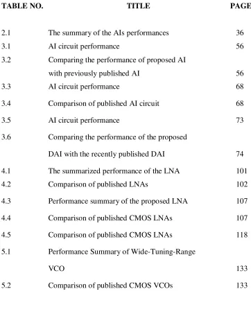
LIST OF TABLES
TABLE NO. TITLE PAGE
2.1 The summary of the AIs performances 36
3.1 AI circuit performance 56
3.2 Comparing the performance of proposed AI with previously published AI 56
3.3 AI circuit performance 68
3.4 Comparison of published AI circuit 68
3.5 AI circuit performance 73
3.6 Comparing the performance of the proposed
DAI with the recently published DAI 74
4.1 The summarized performance of the LNA 101
4.2 Comparison of published LNAs 102
4.3 Performance summary of the proposed LNA 107
4.4 Comparison of published CMOS LNAs 107
4.5 Comparison of published CMOS LNAs 118
5.1 Performance Summary of Wide-Tuning-Range
VCO 133
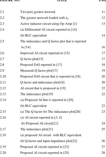
LIST OF FIGURES
FIGURE NO. TITLE PAGE
2.1 Two port gyrator network 11
2.2 The gyrator network loaded with 12
2.3 Active inductor circuit using Op-Amp [1] 13
2.4 (a) Differential AI circuit reported in [14]
(b) RLC equivalent 14
2.5 The inductance and Q factor plot that is reported
in [14] 16
2.6 Improved AI circuit reported in [15] 17
2.7 Q factor plot[15] 17
2.8 Proposed DAI reported in [17] 18
2.9 Measured Q factor plot[17] 19
2.10 Proposed DAI circuit that is reported in [18] 20
2.11 Q factor and inductance plot[18] 20
2.12 AI circuit that is proposed in [19] 22
2.13 The inductance plot[19] 22
2.14 (a) Proposed AI that is reported in [20],
(b) RLC equivalent 23
2.15 (a) The Q factor (b) The inductance plot[20] 23 2.16 (a) AI circuit reported in [3, 4]
(b) Proposed AI circuit[21] 24
2.17 The inductance plot[21] 25
2.18 (a) proposed AI circuit with RLC equivalent
(b) Q factor and input impedance plot[22] 26
2.19 Proposed AI circuit reported in [23] 27
2.21 Proposed AI circuit reported in [26] 29 2.22 Input impedance plot for the proposed AI circuit[26] 30
2.23 Proposed AI circuit reported in [27] 31
2.24 The inductance and Q factor plot[27] 31
2.25 Proposed AI circuit reported in [28] 32
2.26 Inductance plot in strong inversion[28] 33
2.27 Inductance plot in weak inversion[28] 33
2.28 Proposed DAI reported in [29] 35
2.29 Proposed DAI's inductance plot[29] 35
3.1 Active inductor circuit design Flow Chart 39
3.2 Proposed Active Inductor Circuit 41
3.3 Small Signal equivalent circuit 41
3.4 RLC equivalent circuit 45
3.5 Simulated inductance plot 48
3.6 Q factor plot 48
3.7 The simulated inductance plot for = 1 50
3.8 The simulated Q factor Plot for different
configuration ( =13.5kΩ) 50
3.9 The variation of real of input impedance (Z11)
versus Rf (from 2 kΩ to 12 kΩ) 51
3.10 The variation of imaginary of input impedance
versus Rf (from 2 kΩ to 12 kΩ) 52 3.11 The variation of real of input impedance (Z11) versus
Rf for =1.5 kΩ and Rf from 1 kΩ to 10 kΩ 53
3.12 The variation of imaginary of input impedance(Z11)
versus Rf for =1.5 kΩ and Rf from 1 kΩ to 10 kΩ 53
3.13 Inductance plot for =1.5 kΩ and =13 kΩ 54 3.14 Q factor plot for =1.5 kΩ and =13 kΩ 54 3.15 Layout of the Active Inductor (a) With GSG Pad
3.16 Active Inductor circuit 57
3.17 Small signal equivalent 57
3.18 RLC equivalent of AI 60
3.19 The simulated inductance of AI 61
3.20 Quality factor for the AI 62
3.21 Variation of input impedance () by variation
of feedback resistor () 62
3.22 Active Inductor simulated inductance 63
3.23 The highest value of Quality factor plot 64
3.24 Variation of input impedance () by varying the
feedback resistor () at different DC biasing 64 3.25 Inductance plot for another configuration
( = 3.3 kΩ) 65
3.26 Q factor plot for another configuration( = 3.3 kΩ) 65 3.27 Variation of input impedance () by variation of
feedback resistor () for another configuration 66 3.28 layout of the Proposed Active Inductor (a) With GSG
Pad (b) Without GSG Pad 67
3.29 Reconfigurable receiver architecture 69
3.30 Differential Active Inductor circuit 70
3.31 (a) Small signal equivalent (b) RLC Equivalent 70
3.32 Differential inductance plot 73
3.33 Quality factor plot 74
4.1 Reconfigurable LNA architecture 77
4.2 Dual standard LNA 78
4.3 Impedance matching condition 79
4.4 Inductive source degeneration LNA 80
4.5 Thermal noise model for resistor 81
4.6 Thermal noise model for MOSFET 82
4.7 Two- port network 82
4.8 Resistive feedback LNA 84
4.9 Small signal equivalent 85
4.11 LNA circuit 90
4.12 LNA circuit topology based on AI 91
4.13 Proposed complete LNA circuit 93
4.14 Variation of selected frequency band and S21
(Gain) versus 94
4.15 Variation of S21 versus (in simulation rfa1) 94
4.16 Variation of S11 versus 95
4.17 S12 of LNA versus 95
4.18 S22 of LNA versus 96
4.19 NF of LNA versus 97
4.20 NFmin of LNA versus 97
4.21 (a) Tunable PMOS resistance
(b) Selecting frequency band by tuning 98
4.22 Variation of S21 versus 98
4.23 Variation of S11 versus 99
4.24 S22 of LNA versus 99
4.25 NF of LNA versus 100
4.26 NFmin of LNA versus 100
4.27 LNA circuit layout 101
4.28 Cascode amplifier with input and output stage
impedance matching 103
4.29 LNA circuit 104
4.30 , , and of LNA 106
4.31 Noise Figure and Minimum Noise Figure of LNA 106 4.32 A Summary of published topologies of S-to-D-LNA:
(a) Common Source Common Gate (CSCG) configuration; (b) CS amplifier with CSCG balun;(c) differential with ac-grounded second
input terminals 109
4.33 S-to-D-LNA architecture 110
4.34 The proposed S-to-D-LNA circuit 112
4.35 -boosting technique with RC network 114
external capacitor 115
4.37 S21 and S11 plot at 1.57 GHz 116
4.38 NFmin plot at 1.53 GHz 116
4.39 Variation of S21 with variation of from 1 fF
to 250 fF 117
4.40 S21, S11 and NFmin for =121 fF 117
5.1 Passive VCO 121
5.2 Active Inductor based VCO 123
5.3 Schematic of proposed LC-tank VCO based on AIs 124
5.4 VCO output frequency tuning with 126
5.5 VCO Output Power at 1.4 GHZ for =5 kΩ 126
5.6 Phase noise at 1.4 GHz for Rf = 5 kΩ 127
5.7 Output transient signal at 1.4 GHz (mV) for
Rf = 5 kΩ 127
5.8 Output power, phase noise and output transient
signal of the VCO at Rf =200kΩ (f=300 MHz) 128 5.9 Output power, phase noise and output transient
signal of the VCO at Rf =0.5kΩ (f=2.37 GHZ) 128 5.10 VCO Output Power Variations according to Rf
variations 129
5.11 Phase noise Variations according to Rf variations
at 1 MHz offset 129
5.12 (a) Tunable PMOS resistance (b) Variation of
VCO output frequency by tuning Vt 130
5.13 Output power, phase noise and output transient
signal of the VCO at Vt =0.35 V (f=2.05 GHz) 130 5.14 Output power, phase noise and output transient
signal of the VCO at Vt =1.25 V (f=0.275 GHz) 131 5.15 Variation of VCO output power for different
5.16 Variation of Phase Noise for different tuning
voltage () at 1 MHz offset frequency 132
LIST OF SYMBOLS
- Ampere - Voltage Gain C - Capacitor
! - Parallel Capacitance
" - Transistor gate-source capacitance
dB - Decibel
dBc/Hz - Phase noise unit
dBm - Decibel of power referenced to one milliwatt f - Frequency
#$ - Resonance frequency fF - Femto Farad
F - Noise factor g - Conductance
% & - % at '(=0V
% - Output conductance - Transconductance Hz - Hertz
I - Current
) - Input AC current
*,, - - Thermal noise of Load resistor *,. / - Thermal noise of transistor
GHz - Giga Hertz
L - Inductance MHz - Mega Hertz mV - Milli volt mW - Milli watt MΩ - Mega Ohm
- Transistor Number i nH - Nano-Henry
nF - Nano-Farad nm - Nano-meter pF - Pico-Farad Q - Quality Factor
- Resistance Rt - Tuning Resistor
Rs - Serial resistance
! - Parallel resistance - Feedback resistance
45 - Output resistance of transistor
- Scattering Parameters or S-parameters - Output return loss
- power gain - reverse isolation - input return loss T - Temperature (Kelvin)
t - Time
V - Volt
V77 - Voltage Supply v9: - Input AC voltage V; - Tuning Voltage
V<9 - Bias voltage at node i
V9 - Voltage at node i
V=,: - Output referred noise voltage
W;/L; - Transistor width and length Y - Admittance
Yin - Input Admittance
Zin - Input Impedance
B - Angular frequency
B& - Resonance angular frequency
γ - Fitting parameter for the noise model Γ - Reflection Coefficient
Ω - Ohm
C - Pi
LIST OF ABREVIATIONS
AC - Alternative current
AI - Active Inductor
BiCMOS - Bipolar CMOS
CD - Common Drain
CMOS - Complementary Metal-Oxide-Semiconductor
CS - Common Gate
DAI - Differential Active Inductor
DC - Direct Current
FFT - Fast Fourier Transform GPS - Global Positioning System GSG - Ground-Signal-Ground
GSM - Global System for Mobile communications KCL - Kirchhoff's Current Low
KVL - Kirchhoff's Voltage Low LAN - Local Area Network LNA - Low Noise Amplifier
LO - Local Oscillator
MOSFET - Metal-Oxide-Semiconductor Field-Effect-Transistor
NF - Noise Figure
NFmin - Minimum Noise Figure
NMOS - N-channel MOSFET
NR - Negative Resistance
OTAs - Operational Transconductance Amplifiers
PLL - Phase Locked Loop
PMOS - P-channel MOSFET
RFIC - Radio Frequency Integrated Circuit SiGe - Silicon Germanium
SOC - System-On-a- Chip
VCO - Voltage-Controlled Oscillator
LIST OF APPENDICES
APPENDIX TITLE PAGE
CHAPTER 1
INTRODUCTION
1.1 Background
Wireless communication systems are changing fast due to the increasing the demands for high quality wireless devices. Nowadays, the feature sizes of the CMOS devices are decreasing while the operating frequencies of the CMOS devices are increasing. And for CMOS designers, the cost and integration of chip regarding higher performance, small chip area and lower power consumption are challenging task. The expansion of wireless communication systems demands for low cost, high performance and small chip size RF transceivers.
CMOS spiral inductors have effective applications in RF circuits, signal processing and data communications. These applications include Voltage Controlled Oscillator (VCOs), Low Noise Amplifier (LNAs), filters, Phase Locked Loops (PLLs), RF phase shifts and so many applications. But these inductors have some disadvantages. The most important disadvantages are:
1- Low Quality Factor:
increasing the number of turn the chip size and spiral substrate capacitance will be increased dramatically.
2- Large silicon area:
The inductance of a spiral inductor is directly proportional to the number of turns of the spiral of the inductors. For high value of inductor we have to increase the number of turn, and it increases that the chip size. For example, for 8 nH inductance we need 6 turns with = 400 µm. The chip area is larger than 400×400
µ.CMOS active inductors composed of CMOS transistors in special topology that have the inductive characteristic in a specific frequency range.
Active Inductors (AI) in comparison with spiral inductors have advantages such as low chip size, tunable inductance and tunable Q factor. Designing high inductance and high Q factor AI is a challenging task.
If these design issues are solved, the applications of active inductor will be expanded in CMOS RF circuit such as: VCO, LNA, PLL, RF band pass filters, and in many other applications. The applications of active inductors are affected by problems that come from the intrinsic characteristics of MOS devices. The most important of these problems is high sensitivity to noise. It should be considered that this limitation is related to all CMOS devices.
1.2 Problem Statement
circuits do not have a capability of tune ability and reconfigure ability. This is clearly the weakness of these active inductors circuits. Some research work may have improved Q, but circuits do not have tune ability and reconfigure ability. In this case, this active inductor circuit can be used just in specific applications for a fixed value of Q factor and inductance value.
The other important characteristic of active inductors is designing active inductor with high inductivity. In some circuit such as LNA, filter and VCO, using a high inductance inductor is necessary. In designing LNA, the gain is directly related to output inductance. By using active inductor with a high inductance, the total gain will be high and also the frequency range will be reconfigurable. For example, the Q factor could be around 40, but the inductance is low (around 2 nH). In another work, the Q factor is high (around 340), but the inductance is also low (around 1.5 nH). In this case, these active inductor circuits cannot be used in an application such as LNA. Because in some LNA circuit, we need high inductance value. (For example higher than 10 nH).
Q factor is another important parameter in active inductors circuit. In some case, there is a trade of between high Q factor and high inductance value. But the most important aims are high inductance and high tunable active inductors with acceptable Q factor.
Based on the above design issues, the problem statement of this research can be summarized as: Designing high inductance, high tune ability, high Q factor and low power active inductor circuit.
1.3 Objective of Research
The main objectives of this research are three: 1- Designing high tunable active inductor 2- Increase the quality factor
3- Employ the designed active inductors in RF modules, which are VCO or LNA
Design and characterize active inductor circuits which high inductance (from a few nH up to 100 nH) and high tune ability with acceptable Q factor (Maximum value of Q up to 400) and low power dissipation. In the first stage, a study will be conducted on methods to design active inductor circuit and analysis will be carried out on the active inductor’s performance such as inductance, Q factor, tune ability and dc power consumption.
For achieving high inductance value active inductor circuit; we should survey on active inductor structures that have high impedance value. After designing active inductor architecture, we have to set bias condition of active inductor circuit to have a high impedance value.
The tune ability and reconfigure ability is the other performance that should be considered in designing process. The active inductor circuit that has the capability of tune ability, can be used in so many applications such as VCO and reconfigure able LNA. The high Q factor is the other performance of active inductor circuit that should be considered in the design process to achieve acceptable value.
prove that these active inductors are employable. For example, in VCO circuit, we can explain the tune ability of frequency range by tuning active inductor circuit. In the LNA circuit we can show the tune ability of frequency range and reconfigure ability of the circuit by tuning the active inductor circuit core.
1.4 Scope of Study
The scopes of study are as follows:
1. In the first stage of the work, there is a crucial need to make a literature
review of up to date active inductors. After surveying all previous designed and published active inductors, an analysis of major active inductor's performances will be carried out, and it is the task of this research to come out with at least comparable or better performance in terms of high inductance, tune ability, high Q factor and low power dissipation.
The review and analysis could be grouped in to 3 categories:
1- Designing active inductor circuit using reported active inductors topology with improve characteristics. This is possible by changing the active inductors circuit biasing. Because dc biasing is one of the important parts of active inductor design schedules. In active inductor circuit, dc biasing has directly an effect on of transistors and of transistors have most effect on Q factor and inductance parameters. With this reason, by improving the bias condition we can design active inductor circuit with best performance with previously published topology.
2- Designing active inductor circuit using reported topology but by changing or adding some elements to improve the performance of the circuit. By changing some part of topology in sometimes it is possible to improve the performance.
In some case, after surveying all active inductors topologies, it is possible to design active inductor circuit with new topology. By knowing the base of active inductor circuit and by respect to the gyrator concept, it is possible to build new architecture to work as active inductor circuit. In some case, we can conflict two active inductor circuit to make a new architecture with improved performance.
By using one of this three method the active inductors circuit characteristics can be improved.
2. Design Active Inductor architecture
After choosing active inductor design method and architecture, the design process will be started. For analysis of the proposed active inductor circuit, the Cadence software using 0.18 µ m Silterra process was used. During this process all the performances of the designed active inductor will be checked to reach the desired performance of active inductor circuit. If the desired performance of the active inductor is achieved, this step will be finished.
3. Apply the designed active inductor in RF modules.
In this step, the designed active inductors will be applied to the RF modules such as: LNA and VCO to evaluate the performance and applicable of active inductors circuit. Because some of the active inductors have good performance, but they are not applicable in RF modules such as LNA, VCO and filter or other in applications of active inductor circuit.
1.5 Thesis Organization
the active inductor history and advanced active inductors topology. Chapter 3 introduce proposed active inductor circuit. The analysis and the simulation result will be explained in this chapter. In this chapter inductance and Q factor equations will be discussed. In chapter 4, reconfigurable LNA using proposed active inductor circuit will be discussed. LNA circuit will be analyzed and the simulation result will be compared. The tune-ability of frequency range for proposed circuit will be explained. In Chapter 5 the VCO circuit using proposed active inductor circuit will be explained and result will be shown. In chapter 6 the second active inductor circuit will be presented and in Chapter 7 the LNA circuit using the proposed active inductor circuit will be explained. In chapter 8 the third active inductor (differential active inductor) circuit is presented and also it is used in single-to-differential low noise amplifier(S-to-D-LNA) to show the application of this DAI circuit. And finally in chapter 9 the conclusion and some suggestion for future work will be given.
1.6 Contribution of the Thesis
The main aim of this research is focused on a tune-ability of active inductor circuit. Tune ability of active inductors is the main advantage of active inductors that qualified to use it in RF circuit. Because most of the RF circuit such as Filters and VCOs need to use a tunable inductor for frequency band selections. The contributions of this thesis are listed as follows:
i. Propose a first new active inductor circuit topology with wide tuning range (from 1 GHz up to 7 GHz) and high tunable inductance (from a few nH to 100 nH). The best performance of this circuit architecture is high tune-ability and linearity of the inductor for wide frequency range. A feedback resistor is used for tuning the active inductor circuit. Instead of a passive resistor, a PMOS transistor can be used as a resistor to expand the controlling of the active inductor circuit with voltage.
circuit uses current mirror circuit to increase inductance in new circuit topology. The extracted results show that the proposed active inductor has wide frequency range (from 1GHz to 4 GHz), high inductance (few nH up to 600 nH) and low power consumption (lower than 5 mW). In this active inductor topology, the power consumption is lower than the first active inductor circuit and also inductance value is higher than the first one.
iii. Propose a third differential active inductor circuit (DAI). It is designed to work in differential mode. The simulation results show the differential inductance is from a few nH to 500 nH and Q factor from 10 to 200 and power dissipation of 2.2 mW. The proposed DAI circuit is used in single-to-differential- LNA (S-to-D-LNA) to show the performance and applicability of DAI circuit.
iv. Design a reconfigurable LNA based on the proposed first active inductor circuit. In this circuit, the proposed active inductor circuit is used as an output load of the amplifier stage and act as a tunable and reconfigurable inductance. Tuning the frequency range of LNA is possible by tuning the active inductor core. In the active inductor core, tuning is done by using variable passive resistor or variable PMOS resistor. The flexibility of frequency band selection is one of the advantages of this circuit. The other advantages are small chip size and fully inductance-less circuit.
v. Design a wide tuning range VCO circuit using the proposed first active inductor circuit.
In this VCO circuit, the active inductor circuit is used instead of a spiral inductor in general VCO circuit architecture and in this VCO topology, the coarse frequency is achieved by tuning the integrated tunable active inductor circuit. In the active inductor circuit, the variable resistor (passive resistor or PMOS resistor) is used to tune the active inductor core.
REFERENCES
1. Antoniou A. Realization of gyrators using operational amplifiers and their use in RC-active network synthesis. IEE Proc., Vol. 116, No. 11, pp. 1838– 1850, Nov. 1969
2. Fei Yuan. CMOS Active Inductors and Transformers Principle, Implementation, and applications. 2008 Springer, eBook ISBN 978-0-387-76477-1 e-ISBN.
3. Ismail M, Wassenaar R, Morrison W. A high-speed continuous-time bandpass VHF filter in MOS technology. IEEE International Sympoisum on Circuits and Systems. 1991.:1761-1764.
4. Ming-Juei Wu, Jyh-Neng Yang, Chen-Yi Lee. A constant power consumption CMOS LC oscillator using improved high-Q active inductor with wide tuning-range. The 2004 47th Midwest Symposium onCircuits and
Systems, 2004. MWSCAS '04., pp. 25-28, July 2004, doi:
10.1109/MWSCAS.2004.1354366.
5. Thanachayanont a, Payne a. A 3-V RF CMOS bandpass amplifier using an active inductor. ISCAS '98. Proceedings of the 1998 IEEE International
Symposium on Circuits and Systems (Cat. No.98CH36187). 1998;1:440-443.
6. Zhuo W, de Gyvez J, Sanchez-Sinencio E. Programmable low noise amplifier with active-inductor load. ISCAS '98. Proceedings of the 1998 IEEE International Symposium on Circuits and Systems (Cat. No.98CH36187). 1998;4:365-368.
7. Weng RM, Kuo RC. An ω 0 -Q Tunable CMOS Active Inductor for RF Bandpass Filters. Electrical Engineering. 2007:571-574.
8. Thanachayanont a. A 1.5-V high-Q CMOS active inductor for IF/RF wireless applications. IEEE APCCAS 2000. 2000 IEEE Asia-Pacific Conference on
Circuits and Systems. Electronic Communication Systems. (Cat.
9. Ilker Karsilayan a, Schaumann R. A high-frequency high-Q CMOS active inductor with DC bias control. Proceedings of the 43rd IEEE Midwest
Symposium on Circuits and Systems (Cat.No.CH37144). 1:486-489.
10. Ismail M, Olsson H. A novel CMOS fully differential inductorless RF bandpass filter. 2000 IEEE International Symposium on Circuits and Systems. Emerging Technologies for the 21st Century. Proceedings (IEEE Cat
No.00CH36353). 2000;4:149-152.
11. Hsiao C, Member A, Kuo C, et al. Improved quality-factor of 0.18-/spl mu/m CMOS active inductor by a feedback resistance design. IEEE Microwave and Wireless Components Letters. Vol. 12(12), pp. 467-469, 2002.
12. Liang K, Ho C, Kuo C, Chan Y. CMOS RF Band-Pass Filter Design Using the High Quality Active, IEICE Trans Electron, Vol:E88-C; No.12; Page: 2372-2376, (2005).
13. G. Mascarenhas, J. C.Vaz and J. C. Freire. Voltage Controlled Phase Shifters on CMOS Technology, Proceedings of Asia-Pacific Microwave Conference, 2006
14. C.L. Ler, A.K.B. A’ain and A.V. Kordesh. CMOS source degenerated differential active inductor. Electronics Letters. Vol. 44(3), pp. 3-4, 2002. 15. Seo S, Ryu N, Choi H, Jeong Y. Novel High-Q Inductor using Active
Inductor Structure and Feedback Parallel Resonance Circuit. 2007 IEEE
Radio Frequency Integrated Circuits (RFIC) Symposium. pp. 467-470, 2007.
16. Allidina, K.; Mirabbasi, S.; , "A widely tunable active RF filter topology," 2006 IEEE International Symposium on Circuits and Systems, 2006.
Proceedings ISCAS 2006. vol. 4 pp., 21-24 May 2006 doi:
10.1109/ISCAS.2006.1692726
17. Ahmed, A.; Wight, J. 6.7 GHz high-Q active inductor design using parasitic cancellation with process variation control. Electronics Letters. vol.46, no.7, pp.486 -487, April 1 2010 doi: 10.1049/el.2010.3555.
18. Qiang-Tao Lai; Jun-Fa Mao. A new floating active inductor using resistive Feedback Technique. International Microwave Symposium Digest (MTT),
2010 IEEE MTT-S, Vol. 23, No. 28 pp.1748-1751, May 2010, doi:
10.1109/MWSYM.2010.5517785.
Transactions on Circuits and Systems II: Express Briefs, vol.57, no.8, pp.587-591, Aug. 2010, doi: 10.1109/TCSII.2010.2055990.
20. Jeong, Y.-J.; Kim, Y.-M.; Chang, H.-J.; Yun, T.-Y. Low-power CMOS VCO with a low-current, high-Q active inductor. IET Microwaves, Antennas & Propagation, vol.6, no.7, pp.788-792, May 16 2012, doi: 10.1049/iet-map.2011.0332.
21. Anh Bao Nguyen; Jong-Wook Lee. A K-Band CMOS Phase Shifter MMIC Based on a Tunable Composite Metamaterial. IEEEMicrowave and Wireless
Components Letters, vol.21, no.6, pp.311-313, June 2011, doi:
10.1109/LMWC.2011.2138688.
22. Nair, M.U.; Zheng, Y.J.; Lian, Y. 1 V, 0.18 µm-area and power efficient UWB LNA utilising active inductors. Electronics Letters. vol.44, no.19, pp.1127-1129, September 11 2008, doi: 10.1049/el:20081980.
23. Gao Zhiqiang; Xu Honglin; Zhang Zhongzhao; Lan Jinbao. Design consideration of multi-band RF CMOS filter based on active inductors. 2010 10th Russian-Chinese Symposium on Laser Physics and Laser Technologies
(RCSLPLT) and 2010 Academic Symposium on Optoelectronics Technology
(ASOT), pp.341-344, July 28 2010-Aug. 1 2010, doi:
10.1109/RCSLPLT.2010.5615308.
24. Uyanik, H. U. and N. Tarim. Compact low voltage high-Q CMOS active inductor suitable for RF applications. Analog Integrated Circuits and Signal Processing. Vol. 51, No. 3, pp. 191-194.
25. Kumari, K.S.; Bhuvan, B. Compact WiMAX Low Noise Amplifier Using Active Inductor. 2011 International Conference on Devices and
Communications (ICDeCom), pp. 1-5, Feb. 2011, doi:
10.1109/ICDECOM.2011.5738483.
26. Xiao, H. and R. Schaumann. A 5.4-GHz high-Q tubable active-inductor bandpass filter in standard digital CMOS technology. Analog Integrated Circuits and Signal Processing. Vol. 51, No. 1, pp. 1-9.
28. Yushi Zhou, Fei Yuan. Subthreshold CMOS active inductors with applications to low-power injection-locked oscillators for passive wireless microsystems. 2010 53rd IEEE International Midwest Symposium onCircuits
and Systems (MWSCAS), vol. 1, no. 4, pp.885-888, Aug. 2010, doi:
10.1109/MWSCAS.2010.5548661.
29. M. A. Abdelghany, R. K. Pokharel, H. Kanaya, and K. Yoshida. A Low Flicker-Noise High Conversion Gain RF-CMOS Mixer with Differential Active Inductor. Proc. 2009 Korea-Japan Micro Wave Conference, pp. 141-144, April 2009.
30. Hossein Hashemi, Ali Hajimiri. Concurrent Multiband Low Noise Amplifiers- Theory, Design, and Applications. IEEE Transactions on
Microwave Theory and Techniques, Vol. 50, No. 1, January 2002.
31. Chang-Tsung fu,Chun Lin Ko, and Chien-nen Kuo. A 2.4 to 5.4 GHz Low Power Cmos Reconfigurable LNA for Multistandard Wireless Recievers. IEEE Radio Frequency Integrated Circuit Symposium, vol. 68, no. 3, pp.65,68, 2007.
32. Sang-Sun Yoo and Yung-Joun Yoo. A compact Reconfigurable LNA for Single Path Multi-standard Receiver. IEEE Conference onElectron Devices and Solid-State Circuits, 2007. EDSSC 2007. pp.461-464, 20-22 Dec. 2007, doi: 10.1109/EDSSC.2007.4450162.
33. Mohd Tafir Mustafa, A. Zeyegh and T. Z. A. Zulkifli. A Reconfigurable LNA for Multi-Standard Receiver using 0.18µm CMOS Technology. IEEE
Student Conference on Research and Development, 2009, Malaysia.
34. C. P. Moreira, E. Kerherve, P. Jarry, and D. Belot. A Reconfigurable DCS1800/W-CDMA LNA: Design and Implementation issues. Wiley InterScience, 2008.
35. Liscidini A., Brandolini M., Sanzogni D., Castello R. A 0.13 µm CMOS front-end for DCS1800/UMTS/802.11b-g with multi-band positive feedback low noise amplifier. VLSI Circuits, 2005. Symposium on Digest of Technical
Papers. 2005, pp. 406- 409, 16-18 June 2005, doi:
10.1109/VLSIC.2005.1469415.
37. Reja M.M., Moez K., Filanovsky I. An Area-Efficient Multistage 3.0- to 8.5-GHz CMOS UWB LNA Using Tunable Active Inductors. IEEE Transactions on Circuits and Systems II: Express Briefs, vol.57, no.8, pp.587-591, Aug. 2010, doi: 10.1109/TCSII.2010.2055990.
38. Andersson S., Svensson C. A 750 MHz to 3 GHz tunable narrowband low-noise amplifier. NORCHIP Conference, 2005. 23rd , pp. 8- 11, 21-22 Nov. 2005,doi: 10.1109/NORCHP.2005.1596976.
39. Chyuen-Wei Ang, Yuanjin Zheng, Chun-Huat Heng. A Multi-band CMOS Low Noise Amplifier for Multi-standard Wireless Receivers. IEEE
International Symposium on Circuits and Systems, 2007. ISCAS 2007.
pp.2802-2805, 27-30 May 2007, doi: 10.1109/ISCAS.2007.378635.
40. El-Nozahi M., Sanchez-Sinencio E., Entesari K. A CMOS Low-Noise Amplifier With Reconfigurable Input Matching Network. IEEE Transactions
on Microwave Theory and Techniques, vol.57, no.5, pp.1054-1062, May
2009, doi: 10.1109/TMTT.2009.2017249.
41. Geis A., Rolain Y., Vandersteen G., Craninckx J. A 0.045mm2 0.1–6GHz reconfigurable multi-band, multi-gain LNA for SDR. 2010 IEEE Radio Frequency Integrated Circuits Symposium (RFIC), pp.123-126, 23-25 May 2010, doi: 10.1109/RFIC.2010.5477273.
42. Gharpurey R. A broadband low-noise front-end amplifier for ultra wideband in 0.13-µm CMOS. IEEE Journal ofSolid-State Circuits, , vol.40, no.9, pp. 1983- 1986, Sept. 2005,doi: 10.1109/JSSC.2005.848174.
43. Chang-Wan Kim, Min-Suk Kang, Phan Tuan Anh, Hoon-Tae Kim, Sang-Gug Lee, An ultra-wideband CMOS low noise amplifier for 3-5-GHz UWB system. IEEE Journal ofSolid-State Circuits, vol.40, no.2, pp. 544- 547, Feb. 2005, doi: 10.1109/JSSC.2004.840951.
44. Mustaffa M.T., Zayegh A., Zulkifli T.Z.A. A reconfigurable LNA for multi-standard receiver using 0.18 µm CMOS technology. 2009 IEEE Student
Conference on Research and Development (SCOReD), pp.238-241, 16-18
Nov. 2009, doi: 10.1109/SCORED.2009.5443076.
45. Vidojkovic M., Sanduleanu M., van der Tang J., Baltus P., van Roermund A. A 1.2 V, Inductorless, Broadband LNA in 90 nm CMOS LP," 2007 IEEE
Radio Frequency Integrated Circuits (RFIC) Symposium, pp.53-56, 3-5 June
46. Marc Tiebout. Low power VCO design in CMOS, e-book, Springer, 2006 47. Ali Hajimiri, T. H. Lee. The design of Low Noise Oscillator, Kluwer
Academic Publishers, USA, 2003, eBook ISBN: 0-306-48199-5, Print ISBN: 0-7923-8455-5
48. Jenn-Tzey Yang, Shao-Kang Hsieh, and Ping-Jung Tsai. A wide tuning range voltage-controlled oscillator with active inductors for bluetooth applications. In Proceedings of the 4th international conference on Circuits, systems and
signals (CSS'10), Nikos E. Mastorakis, Valeri Mladenov, and Zoran Bojkovic
(Eds.). World Scientific and Engineering Academy and Society (WSEAS), Stevens Point, Wisconsin, 2010, USA, 39-42.
49. Chien-Cheng Wei, Hsien-Chin Chiu, Wu-Shiung Feng. An ultra-wideband CMOS VCO with 3-5 GHz tuning range. Radio-Frequency Integration Technology: Integrated Circuits for Wideband Communication and Wireless
Sensor Networks, 2005. Proceedings. 2005 IEEE International Workshop on ,
pp. 87- 90, 30 Nov.-2 Dec. 2005, doi: 10.1109/RFIT.2005.1598880.
50. Liang-Hung Lu, Hsieh-Hung Hsieh, Yu-Te Liao. A Wide Tuning-Range CMOS VCO With a Differential Tunable Active Inductor. IEEE Transactions on Microwave Theory and Techniques, vol.54, no.9, pp.3462-3468, Sept. 2006, doi: 10.1109/TMTT.2006.880646.
51. Mukhopadhyay R., Yunseo Park, Sen P., Srirattana N., Jongsoo Lee, Chang-Ho Lee, Nuttinck S., Joseph A., Cressler J.D., Laskar J. Reconfigurable RFICs in Si-based technologies for a compact intelligent RF front-end. IEEE
Transactions onMicrowave Theory and Techniques, vol.53, no.1, pp. 81- 93,
Jan. 2005, doi: 10.1109/TMTT.2004.839352.
52. Pascht A., Fischer J., Berroth M. A CMOS low noise amplifier at 2.4 GHz with active inductor load. Digest of Papers. 2001 Topical Meeting onSilicon Monolithic Integrated Circuits in RF Systems, 2001. pp.1-5, 2001, doi: 10.1109/SMIC.2001.942331.
53. Ler Chun Lee, Abu Khari bin A'ain, and Albert Victor Kordesh, Design of CMOS Tunable Image-Rejection Low-Noise Amplifier with Active Inductor,
VLSI Design, vol. 2008, Article ID 479173, 6 pages, 2008.
doi:10.1155/2008/479173
Optical Technology Letters. Wiley Subscription Services, Inc., A Wiley Company, Vol 51 Issue 8 , 2009.
55. Donggu Im, Ilku Nam, Kwyro Lee. A CMOS Active Feedback Balun-LNA With High IIP2 for Wideband Digital TV Receivers. IEEE Transactions on Microwave Theory and Techniques, vol.58, no.12, pp.3566-3579, Dec. 2010 doi: 10.1109/TMTT.2010.2086375.
56. Duan Lian, Huang Wei, Ma Chengyan, He Xiaofeng, Jin Yuhua and Ye Tianchun. A single-to-differential low-noise amplifier with low differential output imbalance. Journal of Semiconductors, Volume 33, Number 3, March 2012, doi:10.1088/1674-4926/33/3/035002.
57. Martins M.A., Pui-In Mak, Martins R.P. A single-to-differential LNA topology with robust output gain-phase balancing against balun imbalance.
2011 IEEE International Symposium on Circuits and Systems (ISCAS), , vol.
15, no. 18, pp.289-292, May 2011, doi: 10.1109/ISCAS.2011.5937558. 58. Ming-Ching Kuo, Chien-Nan Kuo, Tzu-Chan Chueh, Wideband LNA
Compatible for Differential and Single-Ended Inputs. IEEE Microwave and Wireless Components Letters, vol.19, no.7, pp.482-484, July 2009, doi: 10.1109/LMWC.2009.2022142.
59. M.A. Abdelghany, R.K. Pokharel, H. Kanaya, Keiji Yoshida. A low flicker noise direct conversion receiver for IEEE 802.11g wireless LAN using differential active inductor. Microelectronics Journal, Volume 42, Issue 2,
February 2011, Pages 283-290, ISSN 0026-2692,
doi:10.1016/j.mejo.2010.12.005.
60. Kefeng Han, Xi Tan, Zhangwen Tang, Hao Min. A wideband CMOS VGLNA based on single-to-differential stage and resistive attenuator for TV tuners. Journal of Semiconductors, Volume 32, Issue 7, pp. 075003 (2011), DOI: 10.1088/1674-4926/32/7/075003
61. Moo I. Jeong, Jung S. Lee, No C. Myung, Jong M. Kim, Chang S. Lee. A 0.18 µm 3.1–4.8 GHz CMOS wideband single to differential LNA for UWB system. Microwave and Optical Technology Letters, A Wiley Company,17 APR 2009, DOI: 10.1002/mop.24441.
62. Gil I, Cairo I, Sieiro J J. Low-power single-to-differential LNA at S-band based on optimized transformer topology and integrated ESD.
63. A. F. Azevedo, F. Fortes, and M .J. Rosario. A 2.4 GHz monolithic single-ended-input/differential-output low-noise amplifier. Proceedings of the
Conference on Telecommunications, Peniche, Portugal, pp. 68-73, May 2007.
64. Tomás Carrasco Carrillo, José Gabriel Macias-Montero, Aitor Osorio Martí, Javier Sieiro Córdoba, José María Lopez-Villegas. CMOS single-ended-to-differential low-noise amplifier. Integration the VLSI Journal, Volume 42, Issue 3, June 2009, Pages 304-311, ISSN 0167-9260, DOI:10.1016/j.vlsi.2008.11.003.
65. Xiao, Haiqiao, Schaumann, Rolf. A 5.4-GHz high-Q tunable active-inductor bandpass filter in standard digital CMOS technology. Analog Integrated Circuits and Signal Processing, 2007-04-24. Springer Netherlands, Volume: 51,Issue:1,Url:http://dx.doi.org/10.1007/s10470-007-9040-1,Doi:
10.1007/s10470-007-9040-1.