University of Windsor University of Windsor
Scholarship at UWindsor
Scholarship at UWindsor
Electronic Theses and Dissertations Theses, Dissertations, and Major Papers
Winter 2014
Single Electron Devices and Circuit Architectures: Modeling
Single Electron Devices and Circuit Architectures: Modeling
Techniques, Dynamic Characteristics, and Reliability Analysis
Techniques, Dynamic Characteristics, and Reliability Analysis
Ran Xiao
University of Windsor
Follow this and additional works at: https://scholar.uwindsor.ca/etd Part of the Electrical and Computer Engineering Commons
Recommended Citation Recommended Citation
Xiao, Ran, "Single Electron Devices and Circuit Architectures: Modeling Techniques, Dynamic Characteristics, and Reliability Analysis" (2014). Electronic Theses and Dissertations. 5014. https://scholar.uwindsor.ca/etd/5014
This online database contains the full-text of PhD dissertations and Masters’ theses of University of Windsor students from 1954 forward. These documents are made available for personal study and research purposes only, in accordance with the Canadian Copyright Act and the Creative Commons license—CC BY-NC-ND (Attribution, Non-Commercial, No Derivative Works). Under this license, works must always be attributed to the copyright holder (original author), cannot be used for any commercial purposes, and may not be altered. Any other use would require the permission of the copyright holder. Students may inquire about withdrawing their dissertation and/or thesis from this database. For additional inquiries, please contact the repository administrator via email
Single Electron Devices and Circuit Architectures: Modeling Techniques, Dynamic
Characteristics, and Reliability Analysis
By
Ran Xiao
A Thesis
Submitted to the Faculty of Graduate Studies
through the Department of Electrical and Computer Engineering
in Partial Fulfillment of the Requirements for
the Degree of Master of Applied Science
at the University of Windsor
Windsor, Ontario, Canada
2013
Single Electron Devices and Circuit Architectures: Modeling Techniques, Dynamic
Characteristics, and Reliability Analysis
by
Ran Xiao
APPROVED BY:
______________________________________________
Dr. X. Xu
Department of Civil & Environmental Engineering
______________________________________________
Dr. H. K. Kwan
Department of Electrical and Computer Engineering
______________________________________________
Dr. C. Chen, Advisor
Department of Electrical & Computer Engineering
iii
DECLARATION OF CO-AUTHORSHIP/PREVIOUS PUBLICATION
I. Co-Authorship Declaration
I hereby declare that this thesis incorporates material thatis result of joint research, as follows: This thesis also incorporates the outcome of a joint research in collaboration with, and under the supervision of, Professor Chunhong Chen. In Chapters 2 and 3, the key ideas, experimental designs, and data analysis and interpretation were proposed by the author, with the review and revision being provided by Prof. Chen. In Chapter 4, the key ideas and algorithms were presented by Prof. Chen in consultation with the author, and the experimental setup and analysis were completed by the author. Prof. Chen also provided the final review for Chapter 4.
I am aware of the University of Windsor Senate Policy on Authorship and I certify that I have properly acknowledged the contribution of other researchers to my thesis, and have obtained written permission from each of the co-author(s) to include the above material(s) in my thesis.
I certify that, with the above qualification, this thesis, and the research to which it refers, is the product of my own work.
II. Declaration of Previous Publication
This thesis includes one original papers that have been previously published/submitted for publication in peer reviewed journals, as follows:
Thesis Chapter Publication title/full citation Publication status* Chapter 2: Section 2.2
and 2.3.1-2.3.4
Single-Electron Tunneling Based Turnstile: Modeling and Applications, in Proceedings of 2013 IEEE International Conference on Nanotechnology (IEEE-Nano’13), Beijing, China, August 2013.
in press
I certify that I have obtained a written permission from the copyright owner(s) to include the above published material(s) in my thesis. I certify that the above material describes work completed during my registration as graduate student at the University of Windsor.
I declare that, to the best of my knowledge, my thesis does not infringe upon anyone’s copyright nor violate any proprietary rights and that any ideas, techniques, quotations, or any other material from the work of other people included in my thesis, published or otherwise, are fully acknowledged in accordance with the standard referencing practices. Furthermore, to the extent that I have included copyrighted material that surpasses the bounds of fair dealing within the meaning of the Canada Copyright Act, I certify that I have obtained a written permission from the copyright owner(s) to include such material(s) in my thesis.
iv
ABSTRACT
The Single Electron (SE) technology is an important approach to enabling further feature size
reduction and circuit performance improvement. However, new methods are required for device
modeling, circuit behavior description, and reliability analysis with this technology due to its
unique operation mechanism. In this thesis, a new macro-model of SE turnstile is developed to
describe its physical characteristics for large-scale circuit simulation and design. Based on this
model, several novel circuit architectures are proposed and implemented to further demonstrate
the advantages of SE technique. The dynamic behavior of SE circuits, which is different from
their CMOS counterpart, is also investigated using a statistical method. With the unreliable
feature of SE devices in mind, a fast and recursive algorithm is developed to evaluate the
v
DEDICATION
vi
ACKNOWLEDGEMENTS
vii
TABLE OF CONTENTS
DECLARATION OF CO-AUTHORSHIP/PREVIOUS PUBLICATION ... iii
ABSTRACT ... iv
DEDICATION ... v
ACKNOWLEDGEMENTS ... vi
LIST OF TABLES ... x
LIST OF FIGURES ... xi
LIST OF ABBREVIATIONS/SYMBOLS ... xiv
CHAPTER 1 INTRODUCTION AND BACKGROUND ... 1
1.1 Motivation ... 1
1.2 A Brief Introduction of Single Electronics ... 2
1.3 Advantages and Current State of SE Applications ... 3
1.4 Challenges ... 5
1.5 Contributions ... 5
CHAPTER 2 MODELING TECHNIQUE FOR SIGNLE ELECTRON DEVICES ... 7
2.1 Background ... 7
2.1.1 Single electron devices ... 7
2.1.2 Experimental studies and fabrication methods ... 9
2.1.3 Current modeling and simulation methods ... 9
2.2 Method ... 10
2.2.1 Working principle of SE turnstiles ... 11
2.2.2 Verilog-A model and its simulation results ... 13
2.2.3 Temperature effects ... 15
2.3 Application circuits ... 16
viii
2.3.2 Digital frequency divider ... 17
2.3.3 Frequency-voltage level converter ... 19
2.3.4 Phase-frequency detector ... 20
2.3.5 Implementation of the conscience mechanism in competitive learning ... 22
2.4 Summary ... 30
CHAPTER 3 DYNAMIC CHARACTERISTICS AND THE STATISTICAL
MODELING OF SINGLE-ELECTRON BASED CIRCUITS ... 31
3.1 Background ... 31
3.2 Method ... 32
3.2.1 Poisson process ... 32
3.2.2 Proposed statistical method ... 34
3.2.3 Numerical evaluation ... 35
3.3 Examples ... 36
3.3.1 SET-based inverter ... 36
3.3.2 SET-based NAND gate ... 39
3.4 Comparison ... 41
3.4.1 Master equation method ... 41
3.4.2 Monte Carlo simulation ... 42
3.4.3 Macro-modeling method ... 44
3.4.4 The step estimation method ... 46
3.5 Discussion ... 47
3.5.1 The temperature effect ... 48
3.5.2 Non-ideal inputs and multi-stage circuit ... 52
3.6 Summary ... 54
CHAPTER 4 RELIABILITY ANALYSIS OF COMBINATION LOGIC CIRCUITS ... 55
4.1 Background ... 55
ix
4.3 Method ... 58
4.3.1 Equivalent reliability (ER) ... 58
4.3.2 Propagation of Probability and Reliability ... 60
4.3.3 Algorithm ... 68
4.3.4 Time Complexity ... 70
4.3.5 Examples ... 70
4.4 Simulation results ... 74
4.5 Discussion and future work ... 77
4.5.1 Handling gate reliability pair ... 77
4.5.2 Multiple outputs ... 78
4.5.3 Reliability improvement ... 80
4.6 Summary ... 81
CHAPTER 5 CONCLUSION ... 82
REFERENCES/BIBLIOGRAPHY ... 84
APPENDICES ... 91
Appendix A: The Verilog Code of SET-turnstile ... 91
Appendix B: The main part of the ER model (matlab code) ... 92
Appendix C: Copyright Information ... 94
Appendix D: List of Publications ... 95
x
LIST OF TABLES
1.1 Circuit architectures and applications using SEDs 4
2.1 Estimated Performance for a PFD using different Designs 22
2.2 Simulation Parameters of Fig. 2.15 28
4.1 Output Reliability Vector R for Different Gates 62
4.2 Calculation of Kab* 63
4.3 Organizing P0*, P1*, M0 and M1 for 2-Input Gates 64
4.4 Calculation of Equivalent Reliability Pair at Output for 2-Input Gates 64
4.5 Signal Probability and Reliability for C17 with rgate = 0.95 72 4.6 Performance of the ER Model on Small Circuits in comparison with MC simulation (rgate =
0.95) 74
4.7 Comparison of ER Model, PGM and BDEC for Reliability Analysis on ISCAS’85 Benchmark
Circuits with rgate = 0.9 75
4.8 Comparison of ER Model, PGM and BDEC for Reliability Analysis on ISCAS’85 Benchmark
xi
LIST OF FIGURES
1.1 The basic concept of single electron control 2
2.1 Circuit symbol of a single electron tunnel junction 7
2.2 Circuit schematic of (a) SET transistor, (b) SET charge pump and (c) SET turnstile 8
2.3 (a) Circuit schematic of a SET turnstile, and (b) its circuit symbol 11
2.4 Voltage characteristics of the proposed turnstile model at T = 0K 13
2.5 Schematic of a single-electron turnstile followed by a SET transistor 14
2.6 Simulation result for IDS characteristics (T=5K) of Fig. 2.5 14
2.7 The error probability Pthermal 15
2.8 (a) Schematic of a SET turnstile digital FD unit, and (b) its circuit symbol 17
2.9 Simulation results of a 6-division SET turnstile FD unit in Cadence with different duty cycles
18
2.10 SET turnstile FD units used as a frequency-voltage level converter 19
2.11 Simulation results of Fig. 11 for AB = (110) 20
2.12 Schematic of a SET turnstile PFD 20
2.13 Simulation result of Fig. 2.12 in Cadence 21
2.14 Block diagram of proposed conscience mechanism architecture 22
2.15 Proposed circuit structure to implement conscience mechanism 23
2.16 Block diagram of the whole self-organizing neural network 25
2.17 Probability density function of the input data used in exemplar test 25
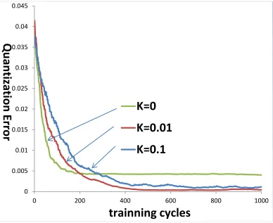
2.18 Performances of learning process with different conscience mechanism strengths 26
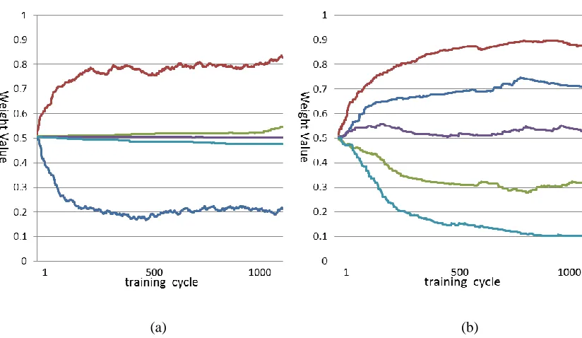
2.19 Weights adaptation process 27
2.20 Transient response of the proposed SET based conscience mechanism circuit 29
xii
3.2 The accurate cumulative distribution and its statistical approximation 35
3.3 The Tucker’s inverter circuit schematic 36
3.4 Comparison of the accurate method and normal approximation in estimating PN(t) 38
3.5 The inverter delay and delay fluctuation range 38
3.6 Circuit schematic of two-input NAND gate using complementary SET transistors 39
3.7 The switching delay of 2-input NAND gate under the worst case and best case 40
3.8 The transient step response of Tucker’s inverter using Monte Carlo simulation 42
3.9 The sample average delay Tavg versus MC trial time k for the Tucker’s inverter 43 3.10 The accurate PDF from the ME and the statistical histogram obtained by multiple runs of
MC simulations 44
3.11 The transient response of Tucker’s inverter to an ideal input signal using the MIB
macro-model 45
3.12 The simulated delay versus load capacitance for Tucker’s inverter 46
3.13 The comparison of delay estimation results for different error probabilities 47
3.14 The simplified state transition diagram 48
3.15 The performance of proposed delay estimation method under different temperatures 50
3.16 Temperature effects on Tucker’s inverter 51
3.17 The CDF of PN(t) for Fig. 3.3 using the solution of Master Equation 53
3.18 The transient response of Fig. 3.3 using the MC simulation 53
3.19 The transient response of Fig. 3.3 using the MIB macro-model 54
4.1 Combinational circuit and its equivalent structure 59
4.2 Probability and reliability propagation for 2-input gate 60
4.3 Dealing with signal and reliability correlation 67
4.4 A special case of Fig. 4.3 68
4.5 An example circuit for independent case 71
xiii
4.7 The output reliability and probability for C17 with different gate reliabilities 73
4.8 The output reliability and probability for C17 with different input probabilities 73
4.9 Simulation results on the overall output reliability of C17 with different values of gate
xiv
LIST OF ABBREVIATIONS/SYMBOLS
Abbreviations:
Abbrev. Description
ADC/DAC Analog-Digital/Digital-Analog Converter
BDD Binary Decision Diagram
BDEC Boolean Difference-based Error Calculator
CCM Correlation Coefficient Method
CDF Cumulative Distribution Function
CMOS Complementary Metal-Oxide-Semiconductor
CNN Cellular Neural Network
ER Equivalent Reliability
FD Frequency Divider
FSB Frequency Synthesizer Block
FSCL Frequency Sensitive Competitive Learning
MC Monte-Carlo simulation
ME Master Equation
MOSFET Metal-Oxide-Semiconductor Field-Effect-Transistor
MV Multiple-Valued
NDR Negative Differential Conductance
PDF Probability Distribution Function
PFD Phase-Frequency Detector
PGM Probabilistic Gate Models
PTM Probability Transfer Matrices
SE Single Electron
SED Single Electron Device
SET Single Electron Tunneling
SN Storage Node
xv
Symbols:
Constants Definition values
e Elementary charge 1.6 10-19 C
kB Boltzmann’s constant 1.3810
-23 J/K
Chapter 1
C Capacitance of the SE island
Ec Charging energy
T Temperature
Chapter 2
C∑ Total capacitance on the SE island
Cext Equivalent capacitance of the reminder of the circuit
viewed from the tunnel junction
CG Gate capacitance of SET turnstiles
CSN Capacitance of SN in SET turnstiles
CT Capacitance of tunnel junctions
d Euclidean distance
K Gain factor of the conscience mechanism
NW Number of wins in the current neuron
Pthermal(t) Probability that a thermal error happens before time
t
qi Charges at the nodes in SET turnstiles
RT Resistance of tunnel junctions
VC Threshold voltage of electron tunnel
Vij Voltage across the tunnel junction
xvi
ΔΕ Electrostatic energy difference before and after the
tunnel event
Г Tunnel rate
Chapter 3
Cload Load capacitance at output node
Gaussian (μ, σ2) Gaussian distribution with the expected value μ and
variance σ2
IDS Current went through the SET transistor
N Total number of states during the logic transition
Ne Total number of tunnel events that need to be
considered within each tunnel junction
Ntot Total electron tunnels happened within each tunnel
junction
Perror, N(TN) Error probability at time TN
Pi(t) Time-dependent occupation probability of state i
Taccurate Delay results from the exact solution of ME
Tapproximate Delay results from the statistical model
Tavg Sample average delay of MC simulation
Teq Delay calculated by step estimation method
ti Arrival time of state i
TMIB Delay calculated by MIB macro-model
Vsw Output voltage swing
Δti Time interval between state i and state i−1
Φ-1
(·) Inverse function of the CDF of a Gaussian variable
Гi Tunnel rate from state i−1 to state i
Chapter 4
xvii {req
0
, req 1
} Equivalent reliability pair for certain signal
{rg0, rg1} Reliability pair of a gate, depending on the error-free
value (“0” or “1”) of its output signal
Fj Primary output of the logic circuit
Kab
* Probability that both signal a and b are “1”
M Probability transfer matrix
M’update Probability transfer matrix for gate reliability pair
Mcor Probability transfer matrix for correlated case
Mind Probability transfer matrix for independent case
P Actual input probability vector
P* Error-free input probability vector
Ps Probability of the signal s being logic “1”
R Output reliability vector
ra’b’(i,j) Probability that both a’ and b’ are reliable
s A specific signal in the combination circuit
s* Error-free version of signal s
εi Error probability of gate i
θ(i,j)
1
CHAPTER 1
INTRODUCTION AND BACKGROUND
1.1 Motivation
It is widely known that the tremendous growth in modern semiconductor industry has been
relied on the continuous shrinking of electronic device dimension over decades. In
microelectronic industry, making things smaller is the most valuable point, since smaller feature
size implies higher computation power per unit area as well as lower cost. However, as the size of
traditional MOSFETs has been scaling down to nanometer, circuit designers are facing new
challenges that were not much critical in the past, for instance, short channel effects, physical
limitations imposed by thermal fluctuations, stochastic nature of quantum effects, large power
dissipation due to leakage and ultrahigh integration densities, and the technological limitation in
manufacturing methods, etc. There have been reports suggesting that the MOS transistor itself
cannot be shrunk beyond certain limits dictated by its operating principle [127]; and according to
the International Technology Roadmap for Semiconductors [1], such rapidly improvement will
eventually come to end in the near future. Therefore, alternative technologies are desired in order
to achieve further scaling and performance improvement. Some novel devices based on new
operation concept and technologies with great scaling potential have been fabricated and under
investigation such as Single Electron Devices (SEDs), resonant tunneling devices (RTDs),
quantum cellular automata (QCA), quantum dots, molecular electronic devices, and carbon
nanotubes or nanowires.
As one of those emerging technologies, SEDs are based on the controllable transfer of single
electrons (SEs) between small conducting electrodes and have had already several demonstrative
scientific experiments as well as enabled fabrication methods. Since electrons were discovered in
1897, people have been trying to build so-called “ultimate circuits” that are able to treat one
electron as one bit information. It is considered as an ultimate target for electronic engineers and
even for the whole information industry, as electrons are the smallest particles that can be
manipulated or controlled with the existing technical conditions. The applicability of single
electronic is wide. For instance, in the field of microelectronic, SEDs are considered as one the
most promising candidate of next generation nanometer devices beyond MOS transistors. The
most predictable and lucrative application is the SE memories, which could store one bit of
information with one electron theoretically; and several companies have single-electron memory
2
like to anticipate that numerous data could be stored in few square nanometers using SE
memories; and the processors using SEs will have extremely high density and computational
capability. Over the decades, engineers and also physicists and chemists were driven to dedicate
themselves to realize these expectations.
1.2 A Brief Introduction of Single Electronics
As the structure size keep scaling into few nanometers, the granularity of charge in terms of
the finite number of charge or electrons need to be taken into consideration. The core of single
electron manipulation is the phenomenon called Coulomb Blockade. Its basic concept is
illustrated in Fig. 1.1 as explained by Likharev in [3], where a conduction island is initially electro
neutral before an extra electron being injected from outside; then this uncompensated single
electron charge will create an electric field which repulses the addition of following electrons.
F
-e
Q=0
F
-e
Q=-e
-e
ε
Figure 1.1. The basic concept of single electron control (after [3]).
It should be noted that the square of the island size has to be small enough to generate strong
electric field that can ensure the SE control. For example, the field is ~140kV/cm on the surface
of a 10-nm sphere in vacuum [3]. More adequate description of this phenomenon is using the
charging energy Ec, as:
2
/ c
E e C
3
where e ≈ 1.6 10-19 Coulomb is the elementary charge and C is the capacitance of the island. If this charging energy is large enough, especially compared to thermal energy kBT, then the single
electron control could be realized; and SE effects could be detected as well.
In order to avoid the disturbance from thermal energy, the Coulomb blockade phenomenon is
commonly investigated and studied either under very low temperature (e.g., ~10K for
100nm-scale devices) or in extremely small structures (smaller than ~1nm for room temperature
operation). This harsh condition is partly the reason for the realization of SE manipulation took
until the late 1980s although its concept has been proposed at very beginning of last century.
However, the rapid growth in nanofabrication techniques recently has made possible the solid
state science field as well as single electronics.
1.3 Advantages and Current State of SE Applications
The advantages of single electronics are obvious, such as low power consumption and
inherent small feature size. Unlike the traditional CMOS where power consumption is mainly due
to the dynamic capacitors charging and discharging and static leakage, SE technique transports
electrons by utilization of electron tunneling phenomenon, which refers to effects manifest in the
injection and extraction of individual electrons from nano-scale structures, and the corresponding
change in energy of system [2]. As the results, logic switching in SE digital circuits could be
completed by only single or several electrons transporting from one electrode to another; and
therefore the energy it consumed is extremely low compare to its CMOS counterpart. It is
understood that in CMOS technology, to conduct a current between the source and the drain, a
voltage in the hundred mV has to be applied to obtain an inversion layer to let the current go
through the transistor; while for SEDs, a supply voltage of few millivolts is enough. For example,
estimated switching energy of single SE logic element is in the order of tens of meV (or, ~10-21J) [68], comparing with fJ~pJ (depend on the load capacitances) for a typical CMOS gate; and for
memory applications, the reported standby power of a hybrid SED/MOS static memory cell is few
nW [39]; for embedded system applications, the simulation results in the literature have shown
that an AVR microcontroller implemented by hybrid SED/MOS architecture consumes
approximately 200uW running at 4MHz, permitting it to run round 20 years on one AA battery
[99].
On the other hand, the nano-scale feature size of SEDs means they will get high integration
density and therefore high computation power for processors, as well as the high storage density
for memory applications. For example, the report from NTT research group showed a
4
that of CMOS implementation [6]. In electronic industry these advantages gives possibilities to
more portable and energy-saving products (e.g., cellphones and tablet computers).
SE technology has also been of much interest for a variety of metrology applications such as
current standards or single-photon sources, thanks to its capability of one by one charge transfer.
It could provide a quantized current depend on the frequency of the electron transfer. This current
quantization has been experimentally demonstrated in Si-wire charge-couple devices [25]. More
applications in terms of current measurement can be found in [35-38].
TABLE 1.1. Circuit architectures and applications using SEDs
SE devices Applications
SE Transistor Logic Gates [70], CNN [92], BDD Logic [80], Embedded system [99]
SE Turnstile Memory [88], Phase Detector [91], Current Meter [36] SE Threshold Gate Flip-flops [68], Majority Gates [71, 100]
SE Trap Memory [43, 44]
Hybrid CMOS-SED ADC/DAC [89], Multipliers [85-87], VCO [90], Binary adder [82], Multiple-valued (MV) Logic [94-95]
Furthermore, SEDs have many novel functionalities such as Coulomb Oscillation coming
from the electron tunneling effect involved. Due to this, SEDs have the ability to efficiently
implement some functions that are inefficient using CMOS logic, threshold logic, or nonlinear
functions [99]. Many novel circuit architectures have been proposed and studied in order to
exploit such special properties. For some applications where the circuits are complex using
CMOS, they may become very concise when SEDs take over, such as multiplexers [99],
multipliers [87], or analog neural networks [101]. Other examples are the SE static memory cell
using its negative differential conductance (NDR) character [44], or ADC/DACs [89] using its
Coulomb oscillation behavior.
Some existing applications using SEDs are listed in Table 1.1, where we can see for each kind
of SEDs there are several applications, including both analog and digital ones. A more detail
5
1.4 Challenges
Although it has promising future, several challenges still remain for large-scale integration of
SEDs and repeatable fabrication method for small feature size products that can work under room
temperature. Certain techniques are also needed for hybrid CMOS and SEDs compatible
integration. SE circuits that operate reliably at room temperature require the critical feature size
less than 10nm, which is also still challenging for repeatable fabrication using existing
lithographic techniques.
On the other hand, SEDs are usually suffered from so-called random background charge
effects which can easily destroy the desired device functionality, especially for memory and
digital applications. This is due to the charged impurities located close to the SE island generated
during the manufacturing process. In addition, the SE effects can be easily influenced by thermal
energy, which means its performance would be temperature depended. In order to avoid the big
performance variation due to temperature fluctuation, certain temperature compensation
mechanism is need (e.g., feedback structures as in [83]); and in terms of SE circuits design, the
robustness against random background charge as well as temperature fluctuation is prerequisite.
The new circuit architectures that have these kinds of features are highly desired for new
generation of SE circuits design.
As a summary, although the SE technology holds great promise, the practical applications
using SEDs would require further research, especially for the fault tolerant techniques,
temperature independent architecture design, and novel information processing architecture which
could take advantages of those SE new functionalities.
1.5 Contributions
In this study, the modeling technique and simulation method have been comprehensively
investigated. A new analytical compact model for one of SEDs, the SE turnstile, has been
proposed. The model is able to accurately describe the tunneling events involved, which is
verified by Monte Carlo simulation with good agreement. Based on the proposed turnstile, hybrid
SED/MOS circuit co-simulations are performed in Spectre simulator on Cadence platform by
implementing the proposed turnstile model in Verilog-A language. By taking advantages of the
frequency characters of SE turnstile, I design several application circuits that could manipulate
signal information in frequency domain, which include the new digital frequency divider, the
frequency-voltage level converter, a phase-frequency detector as well as a conscience mechanism
6
techniques in neural networks by discussing how their drawbacks can be masked in large-scale
parallel computing. A comparative study has been presented to show the efficiency of those new
SE circuit architectures. (Chapter 2)
In order to accurately analyze the switching delay of SE circuit, a statistical method has been
proposed. The switching process within SE logic gates is comprehensively studied; and its
dynamic feature is analyzed theoretically. The stochastic Markov characteristics in electron
tunneling-based systems are investigated, which deduced the proposed statistical delay model.
The effective accurate delay estimation using proposed model is verified by both theoretical
analysis and extensive simulation results. It has been shown that the proposed method has
overcome those drawbacks of existing approaches, which have also been analyzed and evaluated
for comparison study. (Chapter 3)
A novel reliability analysis method, based on concept of equivalent reliability (ER), is
proposed and implemented to evaluate the reliability performance of combinational circuits
consist of unreliable logic elements. The proposed method provides better results than the state of
the art methods in terms of either efficiency or accuracy. Simulation results on several small
circuits and also large scale benchmark circuits show that out approach obtains a significant
speedup over simulation-based methods and more accurate results than other existing analytical
approaches. Based on this new ER model the error propagation in combinational circuits is
studied; and also discussed are its potential applications, including reliability improvement and
7
CHAPTER 2
MODELING TECHNIQUE FOR SIGNLE ELECTRON DEVICES
2.1 Background
In this section, I give some background knowledge regarding to SED such as its basic
components, short history and current frication methods, as well as existing simulation methods. I
start with a brief introduction of the SEDs, followed by a quick review of the history for SEDs
and some recent experimental studies and fabrication method; then I move to an introduction of
the existing modeling and simulation methods for SEDs.
2.1.1 Single electron devices
In order to take advantages of those single electron effects such as the Coulomb blockade,
electron tunneling, and Coulomb staircase and oscillations, many nanoscale systems have been
proposed and studied in the literature. The basic building block of SEDs and circuits is the tunnel
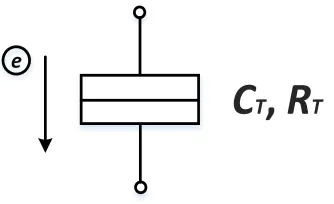
junction, whose circuit symbol is shown in Fig. 2.1, as below.
C
T,
R
T eFigure 2.1. Circuit symbol of a single electron tunnel junction with capacitance CT and resistance RT; an
electron can tunnel through the junction if certain tunnel criteria (which will be discussed in detail in Section 2.2.1) is satisfied.
The tunnel junction is usually recognized as an energy barrier between two electrodes, whose
height and width corresponding to its capacitance CT and tunnel resistance RT, which are the
phenomenological quantities based on the orthodox theory. It should be noted that the tunnel
junction is a representative model for a board range of permeable nanoscale structures fabricated
by different methods on different materials. The electron can tunnel through the junction one by
one if the capacitances of the junction as well as capacitances at two terminals are small enough,
8
which means the voltage across the junction can be changed significantly due to few electron
tunnels. After an electron tunnel happened, the voltage across the junction would decrease then
suppressing the following tunnel events. This is the basic principle how the electron manipulation
can be realized. Such phenomenon is known as so-called Single Electron Tunneling (SET); and
those devices and circuits that utilize SET effects are usually recognized as SET-based devices
and circuits.
R
T,C
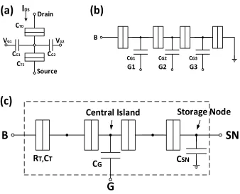
TCentral Island
Storage Node
B
G
SN
(c)
C
GC
SNDrain
I
DSCG2
CG1
VG2
VG1
Source
(a)
(b)
CTD
CTS
B
G2
CG2 CG3
CG1
G3 G1
Figure 2.2. Circuit schematic of (a) SET transistor, (b) SET charge pump and (c) SET turnstile.
Those SEDs composed by tunnel junctions are SET transistors, SET pumps and SET turnstiles,
as shown in Fig. 2.2(a-c), respectively; where those are not shown including resonant tunneling
devices (RTDs) and quantum dots (QDs). The most popular one among them might be SET
transistors consists of two tunnel junctions separated by a nanoscale island to ensure the
occurrence of Coulomb blockade. It has three terminals (viz., drain, source and gate terminals), as
the traditional CMOS transistor; however, its Coulomb oscillation character is unique and useful
for circuit designers.
The SET turnstile is yet another nanometer device that offers a promising way to develop
9
[29] and, since then, various modeling and fabrication techniques have been reported, including
the multilevel memory cell in 2004 [40] and a room temperature data processing turnstile circuit
in 2006 [19]. In the rest of this Section, the SET turnstile is also the main subject of our research
work. For more detail review of SEDs I refer our reader to [4].
2.1.2 Experimental studies and fabrication methods
In 1920s, Robert Milikan showed his famous oil drop experiment which gives possibility to
localize single electrons on oil drop and measure their elementary charge. In 1951, C. Gorter
explained correctly a current suppression at low bias voltage as the cause of Coulomb repulsion
[10]. The electron manipulation of electron in solid material is realized until 1980s. In 1985 D.
Averin and K. Likharev [129] formulated so-called “Orthodox theory” of single electron
tunneling, which quantitatively describes important charging effects such as the Coulomb
blockade and single-electron tunneling oscillation [10]; and the first SET transistor was built by
Fulton and Dolan [128] in 1987. The standard repeatable procedure to build single-electron device
with a double angle evaporation method in the Al/AlO2 material system was also developed by
Dolan [130]. This technique and its variations are still today the most prevalent ones to
manufacture SEDs in metallic material systems [10]. After that, several SEDs and their simple
application circuits with variety of structures or architectures have been proposed and fabricated
based on different procedures and materials [17-38], thanks to the growing studies of production
techniques for small structures.
The recent progress in SEDs manufacturing using electron beam lithography (EBL) is
reported in 2009 [18]. The device dimension of less than 10nm needed for their room temperature
operation is achieved in this work. In 2011, the silicon SET transistor fabrication method based on
optical lithography is proposed by Sun [17] in Singapore. The fabricated SET transistors exhibit
Coulomb oscillation at room temperature due to their extreme small feature size of 4nm. The
optical lithography approach also looks like promising since it is compatible with the
conventional CMOS fabrication process.
2.1.3 Current modeling and simulation methods
The growing studies on single electronics have been made the revolution of microelectronic
industry possible. Since that, the SEDs are more and more involved in the new generation circuit
architecture design. Therefore, the modeling techniques and simulation frameworks of these
SET-based devices are increasingly desired. In terms of SEDs modeling, recently the research on this
10
approaches are currently used for simulation: Monte Carlo (MC) method, Master Equation (ME),
and macro-modeling method. Here, I give a quick review of these three methods; some detail
discussion will also be presented in next Chapter Section 3.4.
The MC method (or, more accurately, kinetic Monte Carlo method) is the most popular
technique. MOSES by Chen et al. [22] and SIMON by Wasshuber [52] are two commonly-used
simulators based on MC method. This approach simulates the electron tunneling events in order
to directly emulate the actual behavior of electrons in SET circuits. In transient simulation, it is
assumed that tunneling events occur instantaneously as a competing Poisson process. In stationary
simulation, a transient simulation is run for a certain number of events per time step. State
probabilities, voltages, and steady currents are calculated as averages over these tunnel events.
The main drawback of MC simulation is that it usually needs large number of simulation trials to
converge into stable and accurate results. Since that, it is only suitable for small scale SE circuits
simulation. Some other simulators based on this method are [57-60].
The ME is the direct description for the underlying Markov process of electron tunneling; and
it is the exact mathematical model for the electron tunneling events involved, which is able to
describe both SEDs static/dynamic characteristics comprehensively. The pioneering simulators
applying this method include SENECA by Fonseca et al. [54] and SETTRAN by Korotkov [3].
The ME simulators are also suffered from the unrealistic long simulation time for even medium
size SE circuits.
On the other hand, the macro-modeling method looks at the macro-characteristics of electron
tunneling, which enable SET circuit simulation using CAD tools (e.g., SPICE) with significant
increase in efficiency for large circuits. For the past few years, this approach is increasingly
employed when simulating SET circuits. While different SEDs need their specific model (e.g.,
single-electron transistors [47-51, 61-64] and turnstiles [53, 91-94]), the macro-modeling method
is very efficient, thanks to the powerful CAD tools. Some existing models can also deal with
certain secondary effects such as background charge and temperature effect. In summary, each of
the above three methods has its own advantages and limitations for static and dynamic
characteristics of SEDs simulations, which inspires us to analyze and evaluate them based on
different performance requirements under different cases.
2.2 Method
In this section, I present a compact model for SET based turnstiles. This macro model is based
11
models (most of them are based on SPICE). This proposed model accurately captures the tunnel
process within the SET turnstile. The device characteristics produced are verified by MC
simulation. The hybrid SET/MOS con-simulations are successfully performed using Spectre
simulator in Cadence platform. In addition, based on the unique functionalities offered by SET
turnstile, some application circuits are designed; and their advantages compared to CMOS
implementations are showed by extensive simulation results.
2.2.1 Working principle of SE turnstiles
SET-based turnstile is a promising device that can accurately transfer single electrons at high
frequency and low power dissipation. Its schematic is shown in Fig. 2.3(a), which consists of four
single-electron tunnel junctions with a bias terminal (B), gate terminal (G), storage node (SN),
and two coupling capacitances CG and CSN.
N1
N2
N3
N4
N5
R
T,C
TCentral Island
Storage Node
C
SNC
GB
G
SN
(a)
(b)
SN
B
G
Source
Figure 2.3. (a) Circuit schematic of a SET turnstile, and (b) its circuit symbol.
The operation principle of the SET turnstile is described briefly as follows. With a proper
value of the bias voltage VB, one or several electrons are pulled into the central island (i.e., node
N3) from the source node N1 (or the storage node SN) by increasing the gate voltage VG beyond a
certain threshold, and then pushed out to the SN (or N1) by decreasing VG. If VG is a periodic
signal, a number of electrons are transferred between the source and the SN over each period. The
direction of electron transfer and the number of electrons transferred during each period depend
12
To model the above turnstile, we assume: 1) the “orthodox theory” of single electron
tunneling is use, 2) the interconnect capacitances are much larger than device capacitances. This
ensures that the device characteristics only depend upon the node voltages, and 3) the initial
charges on all islands in the turnstile are zero, and all tunnel junctions have capacitance CT and
resistance RT. From the turnstile architecture, the charge on node i can be expressed as:
j N
j ij
i
C
V
q
1
(2.1)
where Cij denotes the elements of the capacitance matrix. The voltages and charges on all nodes
(islands) can be derived by solving a set of equations from (2.1) with i = 1, 2, … 5.
The orthodox theory explains how and when the electron will tunnel through the junction,
which is actually due to quantum effect. However, the orthodox theory gives good agreements
with experimental results by using some classical mechanic concepts, certainly by holding some
assumptions and approximations (this is also where its name comes from). In this theory,
tunneling events are modeled as stochastic events, with a certain tunnel rate Γ (probability per
unit time), which depends solely on the reduction of the free energy ΔE of the system as a result
of this tunneling event as given by:
2
[1 exp( / )]
T B
E
e R E k T
(2.2)
where kBT is the thermal energy, e is the charge of an electron, and ΔΕ is the electrostatic energy
difference before and after the tunnel event, and is given by ΔΕ = −e(|Vij|−VC) [68], where Vij is
the voltage across the tunnel junction and VC is the threshold voltage of the junction.
Note that V12 = V23 and V34 = V45 due to the symmetrical structure of Fig. 2.3(a). The above
threshold voltage for an electron to tunnel through a junction is given by:
2( )
C
ext T e V
C C
(2.3)
where Cext is the equivalent capacitance of the reminder of the circuit viewed from the tunnel
junction. When |Vij| > Vc, an electron will tunnel (even at very low temperature) from node j to i
through the junction. This tunnel event will change qi and qj, as well as related node voltages.
The operation of a SET-based turnstile can be viewed as a cycle of electron transfers. When
VG increases from zero to a certain positive value (assume a positive value of VB), an electron
13
after another). When VG returns to a smaller value, the electron starts tunneling from N3 to N1. The transfer cycle is completed as VG returns to zero. As a result, the voltage on the storage node
(i.e., VSN) changes due to the electron charges accumulated at the SN. Here, the VSN is calculated
as:
2
5 3
2 2
2
4(
)
2
[
]
2
4
(
)
G T G T
SN B G
T T T T T G SN T G
C
C
C
C
V
V
V
q
q
C
C
C
C
C C
C
C
C
(2.4)where q3 and q5 (i.e., qSN) are charges on the central island and storage node, respectively.
2.2.2 Verilog-A model and its simulation results
The aforementioned characteristic was described using Verilog-A modeling language, and
simulated under Cadence environment in comparison with SIMON simulator [52]. The
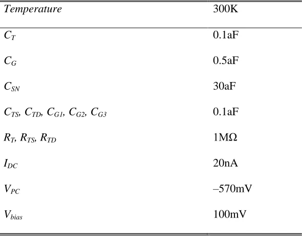
parameters used for simulation are: CT = 1aF, CG = 0.5aF, CSN = 10aF, RT = 1MΩ, VB = 0.1V, and
VG is chosen to be a triangular pulse (it can also be a rectangular pulse without affecting the
tunneling events, as will be seen later in the paper).
V
G
[V
]
V
SN
[
mV
]
0
0 0.5 1 2
25
20
10 15
5
1.5
0.3
0.2
0.1
0 0.4 0.5
Time[s]
Figure 2.4. Voltage characteristics of the proposed turnstile model at T = 0K.
The results are shown in Fig. 2.4, which reveals the accuracy of our model in predicting the
characteristic of the turnstile. I also used a SET transistor which is electrically coupled to the SN
of the turnstile (as shown in Fig. 2.5) to detect its potential change (as an electrometer). The
parameters of the turnstile are same as Fig. 2.4. The input voltage Vin is a pulse signal with
14
1aF, CG =0.1aF, CG2 = 2aF, VDS = 0.02V and the phase-control voltage VPC= 0.04V. The
simulation result is shown in Fig. 2.6. It can be seen that the SET transistor can sense the presence
of single electrons stored in SN. Furthermore, a SET transistor/MOS hybrid circuit can be used to
measure and amplify the voltage level of the SN, which corresponds to the number of electrons
stored in the SN. In this work, the MIB analytical model is used for SET transistors [47].
SN
B
G
VPC
VDS
I
DSV
BV
inCG2
CG1
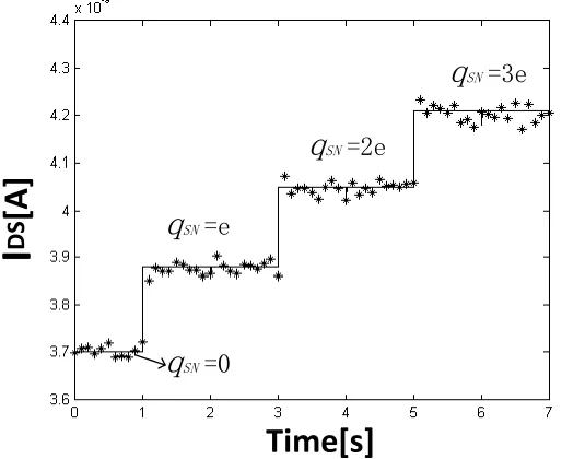
Figure 2.5. Schematic of a single-electron turnstile followed by a SET transistor (used as an electrometer).
Time[s]
I
DS
[A
]
q
SN=e
q
SN=2e
q
SN=3e
q
SN=0
Figure 2.6. Simulation result for IDS characteristics (T=5K) of Fig. 2.5 using SIMON (symbols) and
proposed model (solid line), where the gate voltage of the turnstile is a pulse signal with the period of 2s.
It should be noted that the MC simulation is usually time consuming when it involves
current-biased SET transistors, high temperature and/or high bias voltages for which the number of states
15
efficient to get the same results. One of the key features of Verilog-A model is that, combined
with Spectre, it provides circuit designers with a comprehensive environment for easily
developing proprietary models for specific device behaviors. On the other hand, although the
macro-modeling approach can be used alternatively in a SPICE-compatible environment, it
provides little physical insight into the operation of devices and may not be easily scalable due to
the fact that it is purely empirical in nature [11].
2.2.3 Temperature effects
SET-based devices always suffer from the error tunneling caused by the thermal energy. If T >
0K, the thermal tunnel events take place even if ΔΕ > 0 (i.e., |Vij| < Vc). This is the so-called
thermal error. In Monte-Carlo (MC) simulation [52], the error probability is given by the
following expression:
( ) 1 exp(
)
thermal
P
t
t
(2.5)where Pthermal denotes the probability that a thermal error happens before time t, Г is the thermal
tunnel rate which can be calculated from (2.2).
C
T[aF]Lo
g
10
(P
th
er
m
a
l)
T=40K T=50K T=60K
Figure 2.7. The error probability Pthermal as a function of junction capacitance CT and temperature T.
To explore how the temperature T affects the turnstile circuit, I calculated the Pthermal using
16
increases, so does the Pthermal. The junction capacitance CT is also a key factor. For instance, at T =
50K, Pthermal is about 1e−14 with CT = 0.1aF, and increases to 1e−6 with CT = 0.15aF. In our
model, for each possible tunneling event, we calculate the tunnel rate using (2.2). By considering
the thermal tunnel events as an independent and exponentially distributed process [52], the time
interval between two thermal tunnel events is given by: Δt = −ln(r)/Г, where r is an evenly
distributed random number within the interval [0, 1]. At each iteration, we compare the duration
Δt of all tunnel junctions, and take the shortest one (i.e. a thermal tunneling event happens at this
junction).
2.3 Application circuits
Circuit-level SET turnstile/MOS co-simulations are successfully performed by implementing
the proposed Verilog-A turnstile model in Cadence environment. Analog co-simulations are also
carried out for different application circuits, such as digital frequency divider, frequency-voltage
level converter and phase detector. Furthermore, focus on the application of self-learning network,
I analyzed the impact of using SEDs in its architecture design and discussed the performance of
proposed circuit architecture in terms of area and power consumption.
2.3.1 Reset module
As mentioned before, with a periodic pulse signal of VG in the SET turnstile, one can keep
transferring electrons to or from the SN. The charges that are accumulated at the SN increase until
no more tunneling is possible, depending on the value of VB and VG. For this reason, to ensure the
turnstile can work properly in practice, one usually has to clear the charges at the SN regularly,
which means that a reset module is needed.
To realize the reset operation, a multiplexer can be used with a feedback structure which
controls the select signal. The feedback signal is usually provided by other parts of the circuit
(refer to Fig. 2.8). If its voltage is larger than a certain threshold value, the multiplexer will switch
from VB to a specific voltage Vreset to realize the reset operation. The value of Vreset should be
selected in such a way that the following condition is met:
:|
|
0 :|
|
SN J C
SN J C
if
q
e V
V
if
q
V
V
(2.6)
where VJ is the maximum junction voltage within the turnstile. This implies that electrons can
17
the same circuit parameters as before, let us assume qSN = −e (i.e. an electron stored in SN) in the
first equation above. To pull this electron out from SN, it requires:
2 2 2
(
2
)
4(
)
2
|
|
[
]
2
4
(
)
T G SN T G T G T G
J reset C
T T G SN T G T T
C C
C
C
C
C
C
C
C
V
V
e
e V
C
C C
C
C
C
C
C
(2.7)i.e., VJ = (0.33Vreset+0.016e/CT)> VC, or Vreset > 154.5mV. After clearing the charges in SN, the
second equation in (2.6) must be satisfied to prevent any tunnel event within the turnstile, which
means Vreset < 161.9mV. Generally we can select the Vreset to be (154.5mV+161.9mV)/2 ≈ 158mV.
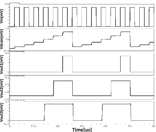
2.3.2 Digital frequency divider
Digital frequency divider (FD) is a commonly used logic circuit, and can be traditionally
implemented by using a series of n D flip-flops (for 2n-division) [107], and each of which consists of 25 or so transistors [15]. When an odd-integer division is required, the circuit could become
more complex with extra logic gates. Alternatively, one can implement the N-divider using a new
architecture based on SET turnstile FD unit (as shown in Fig. 2.8(a)). This unit has a SET turnstile,
a parallel SET/MOS, a threshold comparator, and a reset module. The input signal is connected to
the gate terminal of the turnstile. A parallel SET/MOS circuit is used to measure the charges
stored in the SN. The second gate of the SET transistor is connected to a phase-control voltage
VPC. Due to the constant current bias for MOSFET, the voltage oscillation cross the SET transistor
is amplified to the drain terminal of the NMOS. This drain voltage is sent to both reset and
comparator modules, and the source terminal of NMOS is connected to VSS to bias the transistor at
its sub-threshold region.
VresetVB
VSS
Vdrain
V
outV
inVPC
Idc1 Idc2
MUX SET NMOS
Turnstile SN
B G
Inv Inv
Reset module
(a)
(b)
÷N
IN
O
U
T
CG2
CG1
18
V
o
u
t3
[mV
]
V
o
u
t2
[mV
]
V
o
u
t1
[mV
]
V
d
ra
in
[mV
]
V
in
[mV
]
Time[us]
Figure 2.9. Simulation results of a 6-division SET turnstile FD unit in Cadencewith 1/6, 1/3, and 1/2 duty cycle.
The operating principle of the proposed FD unit is described as follows. Assume the input Vin
is a periodic pulse, the turnstile acts as a digital counter since the potential of SN (and hence Vdrain)
changes discretely with the number of input periods. If N=6 for instance, we set the Vdrain that
corresponds to qSN = 6e beyond the reset threshold. This can be done by adjusting VSS and VPC as
the NMOS operates at the sub-threshold region. Once Vdrain is larger than this threshold, the
multiplexor switches from VB to Vreset. This makes the potential of the SN as well as Vdrain and Vout
return back to their initial values, and the turnstile starts over to count the input periods from qSN =
0. Therefore, for 6 periods of Vin, the FD unit generates one pulse for the output Vout with the
frequency fout= fin/6, where fin is the frequency of Vin. In general, the value of N can be adjusted by
CG2, VPC and VSS. Also, the duty cycle of the output can be anywhere from 1/N, 2/N, …, up to (N–
1)/N by adjusting the threshold voltage of the comparator. Fig. 2.9 shows the simulation results of
a 6-division unit with different duty cycles (the parameters are: Idc1 = 40nA, CS = CD = CG1 = CG2
= 0.1aF, Idc2 = 1uA, Vss = −140mV, Vpc = 578mV, VB = 100mV, and Vreset = −158mV).
Compared with current frequency dividers, the proposed circuit is very compact. A single FD
unit only consists of one SET turnstile, one SET transistor and nine MOS transistors (one NMOS
in SET/MOS circuit, two PMOS as constant current sources, and six transistors in the extra logic).
For instance, to realize 8-division, one needs only one FD unit whose N is adjusted to 8. That
means the whole circuit consists of two SEDs and nine MOSFETs. In contrast, the traditional
19
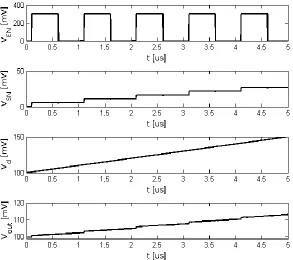
2.3.3 Frequency-voltage level converter
In some circuit applications, the digital information is represented in frequency domain. For
example, in the frequency modulation scheme proposed in [84], the result of a multiplier is
represented as the ratio of the output frequency and a reference frequency (refer to Fig. 2.10).
Frequency Synthesizer
Block
...
c
0c
1c
nfref
A B
Frequency Converter
÷2
IN
O
U
T
D Q
CLK
D Q
CLK
D Q
CLK
...
fout
=(A×B)×
fref
...
Ripple counter
÷4
IN
O
U
T
÷2
nIN
O
U
T
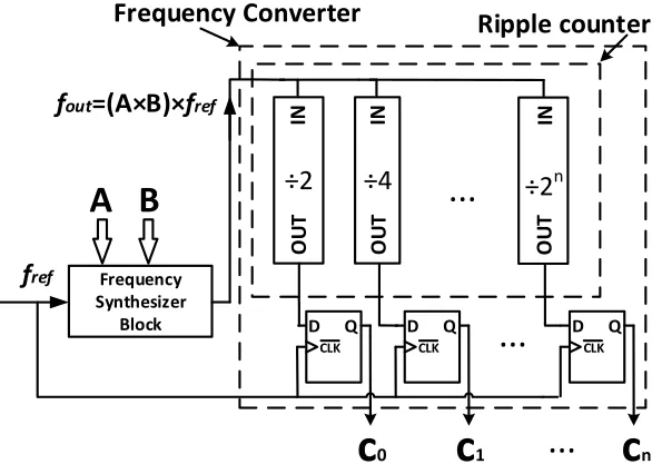
Figure 2.10. SET turnstile FD units used as a frequency-voltage level converter, where (Cn.C1C0)=(AB).
The output frequency of the frequency synthesizer block (FSB) is (AB) times the reference
frequency. To convert this ratio (i.e. AB) to a digital output, a number of SET turnstile digital
FD units are used to implement the frequency-voltage level converter. The proposed converter
consists of a ripple counter and an output module. By connecting these FD units inparallel (set N
= 2, 4, … 2n for FD units where the parameters can be adjusted accordingly as discussed above), the ripple counter counts the number of pulses of the input signal which is connected to the FSB’s
output. The output module consists of several D flip-flops that latch the results from the ripple
counter. The reference frequency is used as a clock signal. Therefore, the binary results reflect the
ratio of fout and fref (or, more specifically, (Cn.C1C0) = (AB)). In real applications, the FD units need to be reset following the output generation. Fig. 2.11 shows the simulation results for AB
20
f
re
f
V
o
u
t0
V
o
u
t1
V
o
u
t2
Time
f
out
0
1
1
Figure 2.11. Simulation results of Fig. 11 for AB = (110).
2.3.4 Phase-frequency detector
SET turnstiles can also be used for implementation of phase-frequency detector (PFD). Fig.
2.12 shows the schematic, which consists of two SET turnstiles and a series SET/MOS circuit as
an electrometer. The bias voltages of turnstiles 1 and 2 are connected to VB and −VB, respectively.
Two pulse signals Vin1 and Vin2 are applied to their gate terminals. One turnstile transfers electrons
at frequency f1, while the other does so at frequency f2. These two processes will conversely
influence the island voltage of the SET transistor that is couple-connected with the two turnstiles.
V
GGVout
Vin
1
Idc
NMOS
SET
-V
BTurnstile2
SN
B
G
Vin
2
V
BTurnstile1
SN
B
G
C
G1
C
G2
21
V
in
1
[mV
]
350
3500
0
1.3 1.7
V
in
2
[mV
]
V
o
u
t
[V
]
Time[s]
0 7
Figure 2.13. Simulation result of Fig. 2.12 in Cadence.
Assume initially there is no extra charge on SN1 and SN2, and that the phase of second input signal Vin2 is ahead. When the falling edge of Vin2 arrives, one electron is transferred to SN2, reducing the potential of SN2. This reduction is detected and amplified by the SET/MOS circuit. Similarly, at the falling edge of Vin1, an electron is pulled from SN1, which increases the potential of SN1. This will make the output voltage go back to its initial value. Therefore, the pulse width of the output voltage of SET/MOS circuit reflects the phase error of the two input signals. The
parameters of turnstiles in Fig. 2.12 are the same as before, and other components are: CS = CD =
CG1 = CG2 = 0.1aF, Vgg = 655mV, and Idc = 50nA which is to bias the NMOS to work at the
sub-threshold region. Fig. 2.13 shows the simulation results.
For comparison, the performance of PFD using different technologies was estimated. The
result is summarized in Table 2.1. In [68], a flip-flop is built using SET transistors and threshold
logic gates, and a PFD is implemented as two flip-flops. In the proposed PFD, it contains two
turnstiles, one SET transistor and two MOSFETs (one NMOS in SET/MOS circuit and one
PMOS as a constant-current source). For the typical current MOS approach [106], a PFD consists
of about 30 transistors. In the proposed circuit, Idc is generically set to about 50nA, and VDD is set
to 1.8V in 0.18μm technology. Thus, the static power is estimated as ~90nW. For a loading capacitance of 1fF at frequency of 500MHz, the dynamic power is nearly 1μW. It can be seen
from Table I that the pure SET circuit consumes extremely low power, but requires more circuit
![Figure 3.3. The Tucker’s inverter circuit schematic. The parameters are the same as in [66], i.e., Vdd =](https://thumb-us.123doks.com/thumbv2/123dok_us/1416016.1174155/54.612.227.418.493.667/figure-the-tucker-inverter-circuit-schematic-the-parameters.webp)