ABSTRACT
SCHABEL, JOSHUA CHRIS. Design of an Application-specific Instruction Set Processor for the Sparse Neural Network Design Space. (Under the direction of Paul D. Franzon.)
© Copyright 2018 by Joshua Chris Schabel
Design of an Application-specific Instruction Set Processor for the Sparse Neural Network Design Space
by
Joshua Chris Schabel
A dissertation submitted to the Graduate Faculty of North Carolina State University
in partial fulfillment of the requirements for the Degree of
Doctor of Philosophy
Computer Engineering
Raleigh, North Carolina
2018
APPROVED BY:
Raju Vatsavai James Tuck
W. Rhett Davis Paul D. Franzon
DEDICATION
BIOGRAPHY
ACKNOWLEDGEMENTS
First of all, I would like to thank my advisor, Dr. Paul D. Franzon, for being supportive and providing the opportunity for multiple rewarding research projects. Second, I would like to thank Dr. W. Rhett Davis for his advice and guidance through many of these research projects. Third, I would like to thank the following faculty: Dr. James Tuck for his mentoring on both the PERFECT and CHIPs projects. Dr. Eric Rotenberg for serving on my masters thesis committee, his mentoring on the PERFECT project, and his computer architecture courses which introduced me to much of the concepts and architectures that have had a direct influence on my research. Dr. Huiyang Zhou for his mentoring on the PERFECT project. Dr. Ginger Yu for putting up with me as the worse TA ever and always being encouraging. Dr. Robert Rodman for serving as my out-of-department committee member in my prelim before his passing, and Dr. Raju Vatsavai for serving as my out-of-department committee member for my final defense.
TABLE OF CONTENTS
LIST OF TABLES . . . .viii
LIST OF FIGURES. . . x
Chapter 1 INTRODUCTION . . . 1
1.1 Overview of the Following Chapters . . . 2
1.2 Abbreviations . . . 2
Chapter 2 Processing Architectures . . . 4
2.1 SIMD Processors . . . 4
2.2 Application-Domain Processors . . . 7
2.3 Processors-in-Memory . . . 7
Chapter 3 State-of-the-ART . . . 10
3.1 SIMD Processors . . . 10
3.2 Application-Domain Processors . . . 14
3.2.1 Reconfigurable Arrays . . . 17
3.2.2 ASIPs Utilizing SIMD . . . 21
3.2.3 Artificial Neural Networks . . . 23
3.3 Processors-in-Memory . . . 26
3.4 Conclusion . . . 28
Chapter 4 The Custom SIMD Processor. . . 30
4.1 The ISA . . . 31
4.2 The Stages of the Pipeline . . . 31
4.3 The Vector Register File . . . 42
4.4 Preliminary Results: The FFT Example . . . 45
4.5 Preliminary Results: Scaling Study . . . 49
4.6 From SIMD to ASIP . . . 54
Chapter 5 An ASIP forSparsey . . . 57
5.1 Baseline . . . 58
5.2 Implementation . . . 61
5.2.1 Step 1 . . . 63
5.2.2 Step 2 . . . 65
5.2.3 Step 3 . . . 66
5.2.4 Step 4 . . . 67
5.2.5 Step 5 . . . 67
5.2.6 Step 6 . . . 68
5.2.7 Step 7 . . . 70
5.2.8 Step 8 . . . 72
5.2.9 Step 9 . . . 72
5.2.11 Instruction-Set Extensions . . . 78
5.3 Results . . . 81
5.4 Summary of Results . . . 88
Chapter 6 An ASIP for HTM. . . 91
6.1 Numenta’s HTM Algorithms . . . 92
6.2 Baseline . . . 97
6.3 Implementation . . . 99
6.3.1 Execution Phase 1 . . . 107
6.3.2 Execution Phase 2 . . . 108
6.3.3 Execution Phase 3 . . . 109
6.3.4 Execution Phase 4 . . . 111
6.3.5 Execution Phase 5 . . . 113
6.3.6 Execution Phase 6 . . . 115
6.3.7 Execution Phase 7 . . . 118
6.3.8 Execution Phase 8 . . . 123
6.3.9 Execution Phase 9 . . . 124
6.3.10 Execution Phase 10 . . . 127
6.3.11 Execution Phase 11 . . . 128
6.3.12 Execution Phase 12 . . . 130
6.3.13 Execution Phase 13 . . . 131
6.3.14 Execution Phase 14 . . . 132
6.3.15 Execution Phase 15 . . . 132
6.3.16 Execution Phase 16 . . . 133
6.3.17 Execution Phase 17 . . . 135
6.3.18 Summary of HTM Steps . . . 138
6.3.19 Instruction-Set Extensions . . . 141
6.4 Results . . . 144
6.5 Summary of Results . . . 152
Chapter 7 The Multifunctional Processor-in-Memory . . . .154
7.1 Related Work . . . 156
7.2 Implementation . . . 158
7.3 Mapping the PIMs . . . 165
7.3.1 5x5 CGRA: "Scatter-Gather" . . . 168
7.3.2 5x5 CGRA: Weight Summation . . . 171
7.3.3 5x5 CGRA: Weight Update . . . 173
7.3.4 5x5 CGRA: Select Winner, LD . . . 175
7.3.5 5x5 CGRA: Select Winner, LE . . . 178
7.3.6 3x3 CGRA: Weight Summation . . . 180
7.3.7 3x3 CGRA: Weight Update . . . 182
7.3.8 3x3 CGRA: Select Winner, LD . . . 184
7.3.9 3x3 CGRA: Select Winner, LE . . . 186
7.4 Results . . . 188
7.4.2 M-PIM vs. PIM . . . 196
7.5 Supporting Parallelism . . . 199
Chapter 8 Conclusion and Future Work . . . .207
8.1 Summary of Contributions . . . 207
8.2 Future Work . . . 208
BIBLIOGRAPHY . . . .209
APPENDICES . . . .216
Appendix A SIMD ISA . . . 217
A.0.1 Explanation of the Instructions . . . 218
Appendix B Additional MPIM Mappings . . . 228
B.1 "Scatter-Gather" SFU for HTM . . . 232
B.2 Weight Summation PIM forSparsey . . . 238
B.3 Weight Update PIM forSparsey. . . 243
B.4 Select Winner PIMs forSparsey. . . 247
B.5 Additional M-PIM Images . . . 253
LIST OF TABLES
Table 2.1 Processor Trade Offs . . . 8
Table 4.1 FFT Twiddle Factor One . . . 46
Table 4.2 FFT Twiddle Factor Two . . . 46
Table 4.3 SIMD for FFT: Area and Energy . . . 47
Table 4.4 SIMD for FFT: Energy-per-FLOP . . . 47
Table 4.5 Process Scaling Study: Area and Power . . . 50
Table 4.6 Process Scaling Study: Power Breakdown . . . 52
Table 4.7 Process Scaling Study: Power Density . . . 53
Table 5.1 The steps ofSparsey . . . 58
Table 5.2 SparseyNetwork Baseline. . . 60
Table 5.3 SparseyStep 1 Results . . . 64
Table 5.4 SparseySteps 2 & 3 Results . . . 68
Table 5.5 SparseyStep 4 Results . . . 69
Table 5.6 SparseyStep 5 Results . . . 69
Table 5.7 SparseyStep 6 Results . . . 70
Table 5.8 SparseyStep 7 Results . . . 72
Table 5.9 SparseyStep 8 Results . . . 73
Table 5.10 SparseyStep 9 Results (LE) . . . 75
Table 5.11 SparseyStep 9 Results (LD) . . . 76
Table 5.12 SparseyStep 10 Results . . . 77
Table 5.13 Sparsey: Latency-per-Frame . . . 82
Table 5.14 SparseyASIP: Area Results . . . 83
Table 5.15 SparseyASIP: Power Results . . . 84
Table 5.16 SparseyASIP: Memory Accesses . . . 85
Table 5.17 SparseyASIP: Instruction RAM Reads . . . 86
Table 5.18 SparseyASIP: SRAM Energy . . . 87
Table 5.19 SparseyASIP: Results Summary . . . 89
Table 5.20 SparseyASIP: Communications . . . 90
Table 6.1 HTM Network Baseline . . . 98
Table 6.2 HTM Memory Requirements . . . 100
Table 6.3 HTM Array Elements . . . 102
Table 6.4 Summary of HTM Steps . . . 138
Table 6.5 HTM Performance Results . . . 146
Table 6.6 HTM ASIP: Area Results . . . 147
Table 6.7 HTM ASIP: Power Results . . . 149
Table 6.8 HTM ASIP: Instruction RAM Reads . . . 150
Table 6.9 HTM ASIP: Data RAM Reads . . . 151
Table 6.10 HTM ASIP: Data RAM Writes . . . 151
Table 7.1 M-PIM Bus Breakdown for PEs . . . 167
Table 7.2 M-PIM Bus Breakdown for Switches . . . 167
Table 7.3 M-PIM Area Results . . . 192
Table 7.4 M-PIM Power Results . . . 193
Table 7.5 M-PIM Area Results . . . 195
Table 7.6 M-PIM Power Results Cont. . . 196
Table 7.7 Breakdown of the results for the PIM and M-PIM in 32 nm for the fourSparsey functions. . . 200
Table 7.8 M-PIM Bus Breakdown for PEs for Parallelism . . . 204
Table 7.9 M-PIM Bus Breakdown for Switches for Parallelism . . . 205
Table A.1 64-bit ISA Breakdown . . . 217
Table A.2 48-bit ISA Breakdown . . . 218
Table A.3 Loads and Stores . . . 218
Table A.4 Data Movement and Synchronization . . . 219
Table A.5 Control Flow Operations . . . 220
Table A.6 Integer Operations . . . 221
Table A.7 Compare Operations . . . 222
Table A.8 Logical Operations . . . 223
LIST OF FIGURES
Figure 2.1 A SIMD Processor . . . 5
Figure 2.2 SIMD Structures . . . 6
Figure 2.3 A Simple PIM . . . 9
Figure 3.1 The Vector-Thread Architecture . . . 11
Figure 3.2 Block Diagram of the ARM NEON SIMD Co-processor . . . 12
Figure 3.3 Block Diagram of the Intel Larrabee Processor . . . 13
Figure 3.4 Predicated Vector Load in Intel Larrabee . . . 13
Figure 3.5 SIMD Challenges . . . 15
Figure 3.6 Flexibility Versus Energy-Efficiency . . . 16
Figure 3.7 Bloack Diagram of the Domain Space Processor . . . 17
Figure 3.8 Bloack Diagram of the ASIP for RSA . . . 18
Figure 3.9 Block Diagram of a CGRA . . . 20
Figure 3.10 Bloack Diagram of the SODA Processor . . . 22
Figure 3.11 Scalar-to-SIMD Operations . . . 22
Figure 3.12 Block Diagram ofAnySP’s SIMD Units . . . 24
Figure 3.13 Block Diagram of the NnSP Architecture . . . 25
Figure 3.14 Bloack Diagram of the OSA+PIMS Architecture . . . 27
Figure 4.1 The Five-Stage Processor with SIMD . . . 30
Figure 4.2 The Fetch Stage . . . 32
Figure 4.3 The Decode Stage . . . 33
Figure 4.4 The Operand Collect Stage . . . 35
Figure 4.5 The Execute Stage . . . 37
Figure 4.6 Block Diagram of Available Functional Units . . . 39
Figure 4.7 The Load-Store Unit . . . 40
Figure 4.8 The Write Back Stage . . . 41
Figure 4.9 Custom Register File: Full-Vector Access . . . 43
Figure 4.10 Custom Register File: Hybrid Access . . . 44
Figure 4.11 The Register File . . . 44
Figure 4.12 SIMD for FFT: Power Breakdown . . . 48
Figure 4.13 A Galaxy of Clusters of SIMD PEs . . . 54
Figure 4.14 32nm PE . . . 56
Figure 5.1 A HierarchicalSparseyNetwork . . . 59
Figure 5.2 SparseyLayer 1 Map . . . 61
Figure 5.3 SparseyLayer 2 Map . . . 62
Figure 5.4 A Simple PIM . . . 65
Figure 5.5 Weight Sum PIM . . . 66
Figure 5.6 The Decode Stage . . . 78
Figure 5.7 The Execute Stage . . . 79
Figure 6.2 Numenta’s HTM: Temporal Pooling Flowchart (LD) . . . 95
Figure 6.3 Numenta’s HTM: Temporal Pooling Flowchart (LE) . . . 96
Figure 6.4 HTM Converging Regions . . . 98
Figure 6.5 HTM to ASIP . . . 101
Figure 6.6 Breaking Up the HTM Structure . . . 102
Figure 6.7 Bitonic Sort . . . 110
Figure 6.8 TTMM Sort . . . 110
Figure 6.9 The Decode Stage . . . 141
Figure 6.10 The Execute Stage . . . 142
Figure 7.1 DySER Block Diagram . . . 156
Figure 7.2 DySER Config FSM . . . 157
Figure 7.3 M-PIM Block Diagram . . . 159
Figure 7.4 DySER Functional Unit . . . 161
Figure 7.5 M-PIM PE . . . 162
Figure 7.6 DySER Network . . . 163
Figure 7.7 M-PIM Switch . . . 165
Figure 7.8 M-PIM Switch . . . 166
Figure 7.9 M-PIM 5x5 Scatter-Gather . . . 169
Figure 7.10 M-PIM 5x5 Weight Sum . . . 172
Figure 7.11 M-PIM 5x5 Weight Update . . . 174
Figure 7.12 M-PIM 5x5 Select Winner with Learning Disabled . . . 176
Figure 7.13 M-PIM 5x5 Select Winner with Learning Enabled . . . 179
Figure 7.14 M-PIM 3x3 Weight Sum . . . 181
Figure 7.15 M-PIM 3x3 Weight Update . . . 183
Figure 7.16 M-PIM 3x3 Select Winner with Learning Disabled . . . 185
Figure 7.17 M-PIM 3x3 Select Winner with Learning Enabled . . . 187
Figure 7.18 M-PIM 3x3 . . . 189
Figure 7.19 M-PIM 3x3 Critical Path . . . 194
Figure 7.20 Processor Trade-offs . . . 196
Figure 7.21 M-PIM 3x5 Weight Update . . . 202
Figure 7.22 M-PIM Block Diagram . . . 206
Figure B.1 M-PIM 4x3 Weight Update . . . 229
Figure B.2 M-PIM 4x3 Weight Summation . . . 230
Figure B.3 M-PIM 4x3 Select Winner, LE . . . 231
Figure B.4 M-PIM 5x5 Scatter-Gather . . . 232
Figure B.5 M-PIM 4x4 Scatter-Gather . . . 235
Figure B.6 M-PIM 3x3 Scatter-Gather . . . 237
Figure B.7 M-PIM 5x5 Weight Sum . . . 239
Figure B.8 M-PIM 4x4 Weight Sum . . . 241
Figure B.9 M-PIM 5x5 Weight Update . . . 244
Figure B.10 M-PIM 4x4 Weight Update . . . 246
Figure B.11 M-PIM 5x5 Select Winner with Learning Disabled . . . 248
CHAPTER
1
INTRODUCTION
Machine learning has evolved in the study of artificial intelligence (AI) as the recognition that AI systems become more robust when granted the ability to extract patterns from raw sensory data to form their own knowledge base, and depends heavily on the representation of the data they are given [41].Artificial nerual networks(ANNs) are a biologically-inspired programming paradigm within machine learning that enables computers to infer rules for recognizing data from the representation of the observational or sensory data they are trained on[57]. ANNs implement learning and inference algorithms as models of neurons and weighted synaptic connections that affect the probability of a result being selected.
differentiated by their learning algorithms, which leads to different paths of implementation and optimization to be explored in this work.
1.1
Overview of the Following Chapters
Design and implementation of a SIMD and PIM optimized ASIP is the focus of this dissertation. Chapter 2 presents a brief introduction into the three main architecture structures utilized in this work: SIMD, ASIP, and PIMs. Chapter 3 presents a discussion on the state-of-the-art in SIMD, ASIP, and PIM architectures. Chapter 4 presents a detailed breakdown of the custom SIMD engine implemented in this work. Chapter 5 discusses the approach utilized in this work for breaking down theSparseyalgorithm for implementation on the SIMD processor, and the benefit of PIM acceleration to this work. Chapter 6 discusses how HTM has been implemented in this architecture, what ISEs have been identified, and how the algorithm was re-envisioned for acceleration on a SIMD architecture. Chapter 7 proposes the multifunctional PIM as a novel element of logic for providing flexibility and reusability to map additional PIMs to the ASIP post-silicon. This dissertation then concludes with a summary of contributions and discussions on future work presented in Chapter 8.
1.2
Abbreviations
µP Mircoprocessor
3DIC Three-Dimensionally Integrated Circuit
ALU Arithmetic Unit
ASIC Application-Specific Integrated Circuit
ASIP Application-Specific Instruction-set Processor
CAD Computer-Aided Design
CGRA Coarse-Grained Reconfigurable Architecture
DSP Digital Signal Processing/Processor
DoSP Domain-Specific Processing/Processor
DSRA Domain-Specific Reconfigurable Array
EDA Electronic Design Automation
FPU Floating Point Unit
FSM Finite State Machine
GPCPU General-Purpose Instruction-set Processing Unit
GPGPU General-Purpose Computing on Graphics Processing Unit
HTM Hierarchical Temporal Memory
ISA Instruction Set Architecture
ISE Instruction Set Extension
LSB Least Significant Bit
LISA Language for Instruction-Set Architecture
LUT Look-Up-Table
M-ASIC Multifunctional ASIC
M-PIM Multifunctional PIM
MSB Most Significant Bit
OTS Off-the-shelf
PCM Phase Change Memory
PIM Processor-in-memory
RA Reconfigurable Array
RRAM Resistive Random Access Memory
SENN Sparse-Encoded Neural Networks
SIMD Single-Instruction Multiple-Data
SoC System-on-Chip
CHAPTER
2
PROCESSING ARCHITECTURES
The final product of this work is an ASIP targeted for acceleratingSparseyand HTM, but can be expanded upon for other ANNs or application-domains of interest. To achieves this, this ASIP must utilize several processing techniques derived from various architectures and computing organizations. This chapter will introduce the computing organizations and architectures utilized in this work.
2.1
SIMD Processors
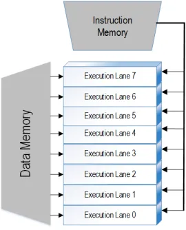
execution paths[47].
Figure 2.1A simple SIMD processor.
In his 1972 paper on computer organizations, Flynn described three basic SIMD processors: array, pipelined, and associative[27]. Flynn described anarray processor, shown in Figure 2.2a, as a number of directly connected, yet independent, processing elements, each with their own registers and local storage, operating only on command from a control unit. An example of anarray processor is the vector-thread architecture[47].
Flynn described apipelined processor, shown in Figure 2.2b, as a time-multiplexed variant of the array processor in which each individual processing element is tailored to a particular function [27]. The control unit then sets up memory for vector operations, and each processing element feeds its results to the next processing element in its pipeline, with the final processing elements streaming the result back to memory. Examples of apipelined processoris the ARM Cortex-A8 NEON Media Engine Unit[16]. Several stream processors for various domain-spaces, such as DSP and ANNs, have been proposed since Flynn’s paper that exploit streaming data between memory and functional-specific processors (the Neural Network Streaming Processors (NnSP)[23]is just one example).
(a)
(b)
(c)
2.2
Application-Domain Processors
ANNs cover several classes of constantly changing algorithms, which is one of the motivating reasons for the implementation of an ASIP in this work. Each new ANN promises some competitive edge over other ANNs and previous implementations of the same ANN. ImplementingApplication-Specific Integrated Circuits(ASICs) for such algorithms is limited by cost and the scope of the algorithm when the ASIC is implemented. By the time an ASIC reaches the market, it is possible for new or improved variations of the algorithms within the application-domain to be available, and the ASIC may have limited capability to support these changes, if any capability at all. Though ASICs can be implemented that allow some levels of programmability and reusability of the network topology, it is difficult and expensive to design an optimal ASIC that could potentially support changes to the functional or mathematical implementation of the algorithms without significant impacts to performance and power.
ASIPs are an emerging architecture concept that targets the area- and energy-efficiency of ASICs with a set level of programmability1and reusability that general-purpose processors (GPCPUs) offer. ASIPs accelerate heavy and highly used functions and bottlenecks in their directed application domain by reducing the pipeline and hardware costs of implementing an assembly instruction set that allows for recompilation of the algorithm for the hardware as changes occur[2, 4, 44, 52, 79]. This is typically done by reducing the overall ISA of a microprocessor (µP) architecture to support a fixed minimal for desired flexibilityand then identifying additional custom instruction-set extensions (ISEs) for calling custom functions for accelerating the algorithm-domain[13, 44, 66, 69]. Table 2.1 shows an abstract view of the trade offs ASIPs offer between general purpose processing and ASICs [79]. ASIPs offer a nice trade off between reusability, flexibility, performance, and power at the cost of additional area and larger software design time. They often do take longer than ASICs to get to market, but can be reprogrammed to implemented changes to the algorithms of interest, whereas ASICs cannot.
2.3
Processors-in-Memory
Previous studies on the sources of energy-efficiency in general purpose processing showed that adding SIMD and VLIW to GPCPUs grants a 10X increase in performance and a 7X decrease in energy; and then adding fused operations grants another 1.4X increase in performance, but still at
1Programmability and flexibility will often be used interchangeably in this work. Flexibility is more general in concept,
Table 2.1Trade offs between general-purpose and application-specific processing[79].
GPCPU ASIP ASIC
Performance low high very high
Flexibility very good good poor
Power very high low very low
Reuse very high high very low
Hardware Design none large very large
Software Design small large none
Market very large large small
Cost software SoC volume
controlled large sensitive
90% overhead for control[38]. What is needed is greater efficiency in processor-memory co-design. In 1970, Harold Stone defined a logic-in-memory computer, in which small functional units were placed inside the cache[71]. The cache structure was broken into sectors, and a sector command is issued, such as asector-add. This operation would then be performed on all the elements defined as operands inside that sector, with the result(s) stored inside that sector. Since 1970, processing-in-memory has remained a controversial concept in computer architecture design. This is largely due to the complications added to memory structures and hierarchies implied in traditional processing-in-memory concepts, such as computational RAM[20].
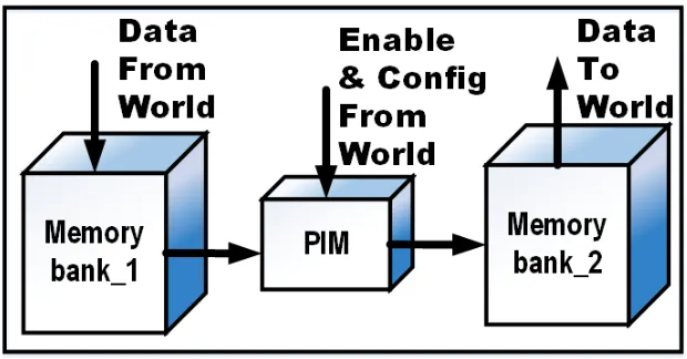
Processors-in-memory (PIMs) has gained attention as a possible solution to theVon Neumann bottleneck(VNB)[8]. The VNB refers to the throttling of processing speeds that arise from the differences between how fast the Von Neumann pipelined processor can run and how fast memory requests can be serviced. In scalar GPCPUs, solutions to the VNB are to add larger caches and larger memory access wordsizes. Parallel processing on many-core networks with advanced cache coherency protocols is another technique at reducing the VBN. PIMs target solving the VBN is two ways:
1. Eliminate the need to move data between the pipelined processor and memory, and
2. Utilization of the the full bandwidth within the banks of the memory.
Figure 2.3A simple PIM.
CHAPTER
3
STATE-OF-THE-ART
In the previous chapter, the computing organizations and architectures utilized in this work were presented. In this chapter, the state-of-the-art of these computing organizations and architectures is presented. For SIMD processors, this will include discussion on the challenges to designing SIMD processors, which is often associated with complications in generalized code and vector data movement. For ASIPs, this chapter will cover a large range application-domain processors, from reconfigurable arrays, FPGAs, and customized SIMD architectures that cover the three basic SIMD structures described in Flynn’s taxonomy[27].
3.1
SIMD Processors
The Vector-Thread Architecture (VTA)[47]is a SIMD-based processor that combines elements of the array, pipelined, and associative structures described in Flynn’s taxonomy[27]. Figure 3.1 shows the abstract model of the VTA. A control core is connected to multiplevector processors(VPs) through a command bus. It issues single commands to all VPs when running in lock-step SIMD, or issues commands to each VP to gather their own instructions, referred to asatomic instruction blocks (ATBs). The control core can synchronize all the VPs via across-VP start/stop queue.
Figure 3.1The Vector-Thread Architecture[47].
each VP’s local registers. These ATBs can be a series of operations that account for a pipelined flow of a given process, ran in lock-step with other VPs, or asynchronized execution for different sized arrays of data. This is achieved by allowing ATBs to have divergent operations that allow each VP to flow down their own execution paths, requesting additional ATBs from the control core. The control core then synchronizes all the VPs when dictated by the program being executed. The VTA is been expanded upon in the Maven Vector-Thread Architecture[50].
Figure 3.2The block diagram of the NEON SIMD co-processor utilized in the Cortex-A7 and A8 architec-tures[16].
expanded to a full media engine with several vector pipelines and data permutations to flush out parallelism at the hardware level[16, 58].
The IBM Cell Processor, utilized in the Sony Playstation 3, included a fully pipelined, 4-way, 128-bit SIMD co-processor with a optimized single-precision fused multiply-add compound instruction [61]. Implemented in 90 nm, this SIMD unit achieved a clock speed of 5.6 GHz, a performance of 44.8 GFLOPs, and a power cost of 43.75 mW/GFLOP.
Intel’s Larrabee is a many-core x86 archiecture for visual computing built upon 16-wide SIMD vector units[10, 68]. The core design of Larrabee is to combine a large L2 cache with several multi-threaded wide SIMD units, all communicating on a wide ring interconnect structure. Each Intercon-nect Access (IA) core included a scalar processor and a 16-wide SIMD unit with separate register files. The block diagram of the Larrabee SIMD unit is shown in Figure 3.3, which includes a full integer and floating point ISA, swizzle data permutations, numeric conversions, and data replication for sharing data across SIMD lanes.
Figure 3.3Block diagram of the SIMD unit inside Intel’s Larrabee[10, 68].
is to keep the SIMD lanes fed in the presence of vector loads and stores where only a few of the lanes may need to access memory. In most SIMD architectures, this would halt the SIMD engine and force the scalar load-store unit to take over to complete the memory accesses of interest.
Larrabee refers to the predicated load access as agather, since non-contiguous (not in order in memory) data elements are being gather from across the memory[28]. The predicated store access is referred to as ascatter, since the array of data elements are not being stored to a contiguous point in memory but instead to various locations in memory. An example of thegatheroperation is shown Figure 3.4.v1is the load result vector that will present the data elements to the SIMD lanes,rax
Figure 3.4Flow of thegatherpredicated vector memory load operation in Intel’s Larrabee[28].
element, andk2is the vector of masks that disable or enable the load operation for each individual data element. First, each element inv3is individually added toraxto calculate its final address to memory. Second, the vector read to memory occurs. Third,k2is checked for each element inv3, and every element with a zero ink2places a zero inv1. The remaining elements place their load results intov1and the results are returned to the SIMD register file.
Intel has implemented a reconfigurable SIMD vector permutation engine for the DSP application-domain[40]. This SIMD engine targets high-performance vector datapaths where SIMD permuta-tions are the bottleneck. These bottlenecks derive from for-loops and array indexing techniques, shown in Figure 3.5a, that are often found in generalized code. These loops induce stalls in vector execution while the data is moved among registers in the register file before the next vector read can occur. Intel implemented a register file that can handle vector reads from non-contiguous data elements in the register file, and then permute the data out into the order the SIMD unit expects it. Intel highlights three non-contiguous read accesses, shown in Figure 3.5b. This includes accessing diagonal elements across the register file bank, accessing "chessboard" elements among adjacent rows in the bank, and strided access across the bank.
Intel’s reconfigurable SIMD engine features a 4-to-32-way reconfigurable vector width, and operates on 32-bit floating point values from 256-bit wide register widths[40]. A 2-dimensional data shuffle of vertical and horizontal functions is integrated into the register file. This serves the purpose of organizing the outputs of the FPUs for storage into the register file for how they will be read back out as operands to different FPUs. The shuffle is broken into two steps to reduce the overall latency: half the shuffle is implemented in write phase, and the second half is implemented in the read out phase. In 22 nm, this SIMD engine achieves a clock frequency of 2.5 GHz at a power cost of 227 mW for both 256-bit byte-wise any-to-any permutes and 64-bit 4x4 matrix transposes.
3.2
Application-Domain Processors
(a)
(b)
for the functional unit includes concepts targeting the trade offs between generality and application-specific functional and arithmetic units, and post-silicon reconfigurability to support updates to functionality in the algorithm of interest (or to support additional algorithms not designed for pre-silicon).
While much of the related work involves utilizing reconfigurable arrays (RAs) of switching logic to achieve both control and functional flexibility, interest into finding "sweet spots" between fully programmable ISA-based processors and ASICs emerged withdomain-specific processing. Domain-specific processors (DoSPs) are optimized for a given subset of algorithms, where the optimization involves investigating the trade offs between the flexibility and generalitiy of GPCPUs, the energy-efficiency of ASICs, and the concept ofreusability, both pre- and post-silicon[1]. An abstract view of the trade-off between felxibility and energy-efficiency in DsOP is shown in Figure 3.6. The goal of DoSPs is to obtain as much energy-efficiency as possible but not to necessarily
Figure 3.6Flexibility vs. energy-efficiency in DoSP[1].
eliminate the instruction stream controlled general-purpose datapath and the flexibility it offers. Instead, DoSP targets minimizing the instruction stream’s overhead to only support what is needed by the application or domain of algorithms of interest for execution on the processor. Reusability is regained by working backwards to decide upon the minimal amount of control and communication primitives needed to support all algorithm domains of interest.
Figure 3.7The reusable DoSP architecture template[1].
with configuring the satellites and communication network to manage the overall control flow. The communications between processors are data-driven, where all processes are synchronized by passing data tokens in a two-phase asynchronous handshaking protocol ("locally synchronous, globally asynchronous").
Abnous and Rabaey show that maximum energy-efficiency is not obtained by only reducing the control overhead of the instruction stream controlled datapath, but by indentifing sources of wasted power in the architecture and designing with eliminating or minimizing those sources [1, 38]. In DoSP, this is achieved through detailed power management. Individual processors are ran at different supply voltages to reduce total switching energy by reducing voltage swing, and unused processors are turned off to eliminate their leakage power. Satellite processors are clustered into local networks to exploit locality of reference and reduce long, global communications. The communication network is segmented into buses of small, less capacitive sections via break switches.
3.2.1 Reconfigurable Arrays
battery-operated (power constrained) embedded systems[46]. Initially, integration of FPGAs into the SoC architecture and design flow was another complicated overhead, but the addition of soft-cores on FPGAs allowed designers to match the ISAs of multiple IP blocks and support custom logic calls from within those ISAs, easing the burden of integrating FPGAs into existing SoCs. Processors of such design have been previously demonstrated with ANNs[66], PIONEER[43], and on several FPGA custom processors[70].
Shrimal and Jain[70]have presented a discussion on instruction customization for ASIP realiza-tion. They discuss the challenges of creating ISEs for custom logic amid the hard constraints of of µPs, such as register file size, cache memory size, and functional unit bandwidth. This motivates the claim that soft-processors on FPGAs are ideal for implementing ISEs for custom logic as the soft-processor handles the constraints ofµPs. Shrimal and Jain[70]then compare the differences between the advantages and disadvantages of ISE customization in three soft-processors: the Altera NIOS II, the Xilinx MicroBlaze, and the Tensilica Xtensa. The authors conclude that the energy-efficiency of FPGAs remains the leading factor against utilizing soft-processors on FPGAs for ASIP architectures.
An ASIP for RSA cryptosystems has been presented by Want et al.[75]. Their ASIP is presented as a three-stage pipeline, shown in Figure 3.8, with a stripped down ISA for only supporting pro-grammibility within the algorithm domain. This includes arithmetic operations (add, sub, multiply,
Figure 3.8Block diagram of the RSA ASIP architecture[75].
addition-with-carry, and subtraction-with-borrow). The RSA domain-specific operations are im-plemented as custom logic to fit the specifications of the algorithms for speedup and efficiency. Implemented on a Xilinx Virtex5 LX110T FPGA, the authors report that adding the RSA domain-specific operations to their ISA on average grants a 2.6X-2.8X speedup, but conclude that greater speedup and efficiency could be with a highly parallel architecture for RSA.
As an alternative to generic FPGAs,Domain Specific Reconfigurable Arrays(DSRAs) have been presented for motion estimation[45], distributed arithmetic operations[46], and for generic FSM operations[53, 54]. DSRAs extend the ideas of DoSP proposed in[1]by exploiting two observations: • Most applications that would utilize reconfigurable arrays (RAs) use them for very specific
calculations that are known to the designer before implementation[46].
• Low-level, fine-grained optimization of the flexibility to these specific calculations can de-crease the area and power overheads significiantly[45].
A DSRA for distributed arithmetic operations has been presented by Khawam et al.[46]. This DSRA is implemented as an SoC comprised of several IP-blocks (GPCPUs/µPs), DSP engines, and several embedded RAs (incorporated as synthesizable soft-cores). Each RA is implemented for a specific computation in the targeted application, with specific arithmetic units (shift registers, accumulators, and adders). Multiplication tasks are optimized out of the ALUs by pre-calculating all possible multiplication results and storing them in look-up-tables (LUTs), which can be updated post-silicon. Arithmetic units are organized into clusters via configurable switches, which can change how the arithmetic units feed into one another, providing marginal post-silicon functional flexibility and reusability. Clusters are then connected via basic mesh interconnects for additional flexibility.
FLEXDET, a reconfigurable ASIP (rASIP) for multi-mode MIMO detection, is presented by Chen et al.[12]. FLEXDET utilizes a 4x4Coarse Grained Reconfigureable Array(CGRA) to execute the various matrix multiplication operations found in the domain-space (as compared to the SIMD-based approach presented in PEPSC[17]). The CGRA, shown in Figure 3.9, is comprised of several processing elements (PEs), which each contain complex1multipliers, ALUs, a bit shifter, and a logcal register file. PEs are organized into cluster for data permutations. To form the rASIP, the CGRA
Figure 3.9Block diagram of the CGRA implemented in FLEXDET[12].
is accommodated by control core based on the RISC ISA, compiled by LISA[39]. The control core serves only two purposes: 1) keep the memories up-to-date, and 2) synchronize and configure the individual PEs of the CGRA for execution. The matrix operations of the CGRA are added as ISEs to the control core, and the CGRA is enabled by the instruction-decode stage of the control core, with results returned to the register-file-write-back stage.
An ASIP for Two dimensional Discrete Fourier Transform (DFT) and Discrete Cosine Transform (DCT) is presented by Pivezhandi and Eshghi[62]. Pivezhandi and Eshghi first discuss how ASIP toolkits, such as LISATek[39, 56], which offer faster times to market and simple-to-use models for utilizing VLIW, SIMD, and RISC ISAs, but often struggle to meet the desired power and performance.
To implement the DFT and DCT, Pivezhandi and Eshghi identify a small list of instructions their ISA must support: addition, subtraction, decrement, increment, module, multiply, multiply-accumulate, AND, OR, XOR, NOT, shift right logical, shift left logical, barrel shift right, and barrel shift left. They then introduce two higher level instructions, DFT02 and DCT02, for implementing large chains of fused operations. The ASIP centers around an RA of address generators constantly working to to keep the memory units streaming to the functional units, which keep their workloads stored in a local instruction memory structure.
3.2.2 ASIPs Utilizing SIMD
There are several variations on ASIP architectures for digital signal processing (DSP). These archi-tectures typically target acceleration of custom vector engines and fused operational blocks called via very-long instruction word (VLIW) extensions supported in the ISAs of many off-the-shelf (OTS) GPCPUs andµPs[38]. This concept dates to DoSPs but has been more previously demonstrated in SODA[51], AnySP[78], Ardbeg[77], PEPSC[17], and the vision processing SoC[80], and are of increasing interest to EDA CAD tool providers, such as Synopsys[3].
The Signal-processing On-Demand Architecture (SODA) is a fully programmable CGRA that utilizes an ARM Cortex-M3 and a 32-wide custom SIMD pipeline[51]. SODA targets acceleration of the software defined radio (SDR) domain-space, with an emphasis on the high data parallelism inherent within the domain-space. This high data parallelism is accompanied by data permutations, scalar-to-vector, and vector-to-scalar operations that can slow down vector execution. The block diagram of the SODA architecture is shown in Figure 3.10a. For flexibility, SODA utilizes a 400 MHz ARM Cortex-M3µP. The ARMµP can call the PEs utilizing its embedded VLIW support. Each processing element (PE) includes a local memory and an execution unit (EU). Each EU includes a scalar core and a SIMD core, along with a WtoS and StoW unit. Each SIMD unit contains a 16-entry register file, 16-bit ALU with multiplier, and a port on a SIMD Shuffle Network (SSN) for data-permutations. The SSN, shown in Figure 3.10b, is a configurable data permutation network that allows the mapping of multiple permutation paths across the SIMD lanes.
(a) (b)
Figure 3.10a) The SODA block diagram and b) the SODA SIMD Shuffle Network implemented in SODA
[51].
AnySPis an extension to SODA that targets acceleration and optimization of any signal processing algorithm-space, beyond just SDR, presented by Woh et al.[78]. First, AnySP targets a variable SIMD width, dynamically determined by the algorithm of interest during execution. Second, AnySP targets register file waste in the SIMD by splitting the register file into small and large regions, where only the most commonly used variable are stored within the smaller, faster, and lower-power register file. Third, AnySP targets optimization through instruction pairing (also known as fusing operations). They observe that in most signal processing domains, most operations occur in patterns. Most notable of these are purmute-add, add-add, multiply-add, and shift-add. They then observe that these instruction pairs also occur in pairs, such ass add-add followed by shift-add. Utilizing the VLIW support in the ARMµP, it is possible to continuously fuse such operations together with minimal instruction-support overhead. Fourth, AnySP exploits the fixed set ofswizzleoperations found within most signal processing domains, which includes data permutations and replication of data. Custom ISEs are implemented to call and configure each of these swizzle operations. Further data permuations are supported by a crossbar in the SIMD execution lanes (shown as theXbarin Figure 3.12). This crossbar allows data movement to be fused with individual functions in each SIMD’s Flexible Functional Unit (FFU), and possibly between individual functions across SIMD lanes.
Ardbeg is another extension on SODA for commercial use presented by Woh et al.[77]. Ard-beg derives its ISA from the ARM NEON co-processor extentions, and was built utilizing the ARM OptimoDE framework[14]. OptimoDE is a configurable VLIW-style Data Engine architecture for intensive data processing, with unlimited data path configuration options and user defined ISE customization. OptimoDE utilizes data subgraphs to identify potential custom logic and ISE exten-sions, including instruction-pairs and fused operations. Ardbeg distinguishes itself from SODA and AnySP by identify the most computationally intensive algorithm within SDR: W-CDMA. W-CDMA is also the most difficult algorithm in SDR to vectorize on their SIMD since vectorization requires con-current memory accesses for larger vectors, thus the serialized memory accesses in SODA become the bottleneck. After attempting software pipeling to ease the issue, the Ardbeg designers propose a full ASIC for W-CDMA, called as a custom ISE.
Ardbeg is the first example of utilizing ISEs to call full custom logic processors and not just reconfigurable arrays of arithmetic units. Another example is the SoC for vision processing presented by Zhang et al.[80]. This processor utilizes VLIW within a 32-bit RISCµP to call several ASICs for specific operations in the vision processing domain. The individual ASICs included are a difference image unit, an edge image processing unit, and a threshold computing unit.
3.2.3 Artificial Neural Networks
the implementation of various ANNs of various topologies that groups configurable processing elements (PEs) into streaming units that rapidly stream workloads and results in and out of local caches[23, 24]. The NnSP architecture is shown in Figure 3.13. NnSP utilizes a high level arbiter
Figure 3.13Block diagram of the NnSP architecture, its processing units and processing elements[23, 24].
unit monitoring and providing work loads to several processing units (PUs) and memory structures. Each PU is comprised of a cache and several processing elements (PEs). Each PU is handed a task with start locations in memory. The PU breaks these tasks down into workloads, streams the data into its cache, and sends the workloads out to PEs. The PEs then stream their data from the cache and execute their individual workloads, asynchronously. When a PE is complete, it streams its result to the cache and requests another workload. When a PU is complete, it streams its results to its larger memory structure and requests another task for processing. The PEs are rather generalized and can be configured to support a multitude of ANNs, though typically only the inference stage algorithms.
An ASIP for bidirectional associative memories and Hopfield auto-associative memories has been presented by Shapiro et al.[69], though their work focuses more on their algorithm for au-tomating identification of custom ISEs utilizing sub-flow graphs for discovering basic functional blocks that could be implemented as fused operation blocks called with the ALU to accelerate data paths within unrolled nested for-loops. Their algorithm focuses purely on highly used functional paths within an algorithm but is unable to determine bottlenecks due to functional complexity, memory bandwidth limitations, or interconnect bandwidth limitations.
custom logic (flashed to the FPGA with the soft-core), a speedup of 50X is achievable over just running the inference algorithm in the FPU. The primary custom ISE is for implementing thetanh activation function.
3.3
Processors-in-Memory
Computational RAM (C-RAM) iis a PIM architecture implemented in a DRAM process at the IBM foundries[20, 21]. The goal of C-RAM was to integrate several SIMD processors on the same die as DRAM, pitch-matching the processing elements ot the memory columns, and then control the processors from a control core implemented on separate die of logic-optimized silicon. C-RAM can be operated as any of the three SIMD types (array, pipelined, and associative) from Flynn’s taxonomy[27]. C-RAM also sought to preserve and exploit native feature of the memory and the open bandwidth across the banks.
A distributed multiple-SIMD PIM for Parallel Processing in Memory (PPIM) has been imple-mented that targets matching the DRAM memory organization to the access patterns required by program being executed to the multiple-SIMD units[64]. This is achieved by adding multiple controllers that can adjust the numner of SIMD units under their control dynamically according to the needs of the program. These controllers can also adjust the clock speeds of the SIMD units to match the latency of the access patterns, thus reducing power when possible, or increasing when needed.
Video-Active RAM (VA-RAM) is an PIM architecture for the video encoding application-domain space[67]. The VA-RAM architecture consists a large embedded SRAM that is address by a horizontal address decoder, which reads an entire row at once. The data is read out to a data distributor, which distributes the data out to all of the PEs. The PEs operate in parallel (SIMD), and are implemented specifically for a certain class of multimedia applications.
A PIM architecture for accelerating the cryptography application-domain space has been pre-sented by Chang, Liu, and Gaudiot[11]. They target the cryptography applicaiton-domain space since data encryption and decryption algorithms require many arithmetic and logical operations to be executed, with a large amount of memory accesses. The PIM architecture is pursued as it:
1. reduces the penalty caused by an excessive amount of memory accesses among a limited amount of transferring bandwidth between the processor and memory, and
2. exploit the inherent parallelism within the algorithms.
Optimal Adiabatic Scaling (OAS) is a concept introduced to increase performance efficiency while utilizing existing technologies[18]. OAS combines the power efficiency of adiabatic circuits with 3D scaling to target application-level parallelism.Adiabatic circuitsdefine a class of circuit design where energy per gate operation is proportional to clock rate, of which the authors of OAS utilize to define new rule for semiconductor scaling2. 3D stacking is utilized in OAS to reduce wire lengths, decrease power for long transmissions lines, decrease the latency between processors and memory, and open up the bandwidth between processors and memory. As OAS circuits scale, computational throughput increases and clock rates drop with the square root of the growth of the number of devices. As traditional von Neumann GPCPUs cannot utilize this growth in computing throughput, largely via parallelism with wide memory bandwidth requirements, Processor-in-Memory-and-Storage (PIMS) is introduced as a PIM architecture to exploit this increase in computing throughput [18]. PIMS is implemented in non-volatile devices (RRAMs and PCMs), targeting problems associated with data in storage only. The OAS+PIMS concept is shown in Figure 3.14, which is shown as a single-tier or processing elements stacked underneath a 3D stack ofadiabatic memory. The PIMS
Figure 3.14The OAS+PIMS architecture of 3D stacked memory and replicated PIM units[18].
architecture divides the processors intostreaming processorsthat are each connected to dedicated banks of memory in the 3D stack, and is described as a non-von Neumann architecture where each individual PE operates asyncrhonously, as triggered by the data assigned to it (similar to an associative SIMD processors from Flynn’s taxonomy[27]).
2Scaling that is based on unchanging devices, where they consider scaling at a single given technology node, not
3.4
Conclusion
In Chapter 4, design and implementation of the custom, instruction-extendable SIMD processor presented in this work will be explored. In Chapters 5 & 6, utilization of this SIMD processor as the building blocks of our ASIP for two sparse neural networks (SpNNs) will be explored, focusing on the iterative process of implementation and optimization of the algorithms for the SIMD processor to identify custom ISEs to add to the SIMD’s ISA for accelerating performance. This work builds on several of the processing concepts and architectures discussed in this chapter (along with Chapter 2). A summary of these concepts include:
• Similar to several of the ASIPs for DSP applications implemented as arrays of SIMD processors, this work implements a hierarchical array of SIMD units with custom logic called by ISEs for accelerating the application-domain of interest. This work pulls from many of these ASIPs to identify several data permutation and shuffle patterns that are common to SIMD execution. ISEs are added to support these data permutation and shuffle patterns.
• For processing the SpNNs, this architecture executes in phased-based processing, where each phase is either a processing phase (of a single function) or a communications phase. Each execution phase is implemented with phase blocking in mind, which implies that an entire execution phase must complete before any SIMD starts executing the next phase. Similar to the VTA[47], when utilizing multiple SIMD units within aclusterto execute a phase, this architecture utilizes a control core to start the units in lock-step. During the processing of the phase, each SIMD can diverge down its own paths as the data directs, but the control core is responsible for synchronizing all SIMD units for the next execution phase.
• The ring-based network for communication phases implemented in this work is in part based on the token-ring memory bus implemented in the IBM Cell Processor[61].
• This work utilizes per-lane predication for accelerating the SpNNs to deal with vector execution on uneven vectors (vectors not divisible by widht of the SIMD unit). This is implemented in a similar fashion as implemented in Intel’s Larrabee SIMD processor[10, 28, 68]by utilizing bit masks for nullifying the data on lanes not working on a valid element in the vector. Larrabee nullifies such data after loading from memory. This work targets nullifying the data and addresses to memory before loading from memory to reduce the energy costs of unnecessary data accesses.
divergent to map well to the SIMD processor, resulting in purely scalar execution with negative impacts on performance or energy-efficiency. The second reason is that the data the function is operating on is so large that 20-50X more time is spent moving the data during the function rather than performing useful work. Implementing these functions as PIMs reduces the time it takes to move the data between the memory and processing element, and allows for much rapid execution through the function without instruction and pipeline overheads.
CHAPTER
4
THE CUSTOM SIMD PROCESSOR
The basic processing unit implemented in this work is a five stage scalar processor, shown in Figure 4.1. The stages of this pipelined processor include fetch, decode, operand colllect, execute, and write back. The execution stage in this processor has been implemented as a SIMD execution path. The register file is custom implemented for vector access for the SIMD execution path, including three modes of instruction-configurable access.
4.1
The ISA
The ISA currently implemented in this architecture is derived from the 64-bit NVIDIA FERMI ISA [6, 7, 76]. Though the naming conventions of the ISA breakdowns, including the instruction type and individual instruction specifiers (name_a,name_b) are still utilized, much of the structure of the ISA has been changed to meet the needs of the processor, and to simplify the decode logic in the processor to reduce power. The ISA currently has twovariations on instruction width (48-bits and 64-bits), each investigated in this architecture to work with multiple wordsizes (8-bits, 16-bits, 32-bits, and 64-bits). A full breakdown of the ISA is provided in Appendix A. Appendix A also provides the ISA to-date, excluding any instruction set extensions (ISEs) that have been added to support Sparseyand HTM, which will be discussed later in this chapter.
The 64-bit ISA (ISA64) was initially implemented a 32-bit wordsize (32WS) architecture that could accomidate operations with 1-3 operands or one operand and a 32-bit immediate. The ISA64 could also support 64-bit integer and floating point operations with 1-3 operands, but no operations involving a 64-bit immediate. The 48-bit ISA (ISA48) was implemented to accommodate the 16-bit wordsize (16WS) architecture. In this architecture, only 16-bits are needed to support operations with an immediate, and the additional 16-bits is removed from the instruction width. The 16WS architecture includes additional load and store operations to accommodate for a 32-bit address space to memory since 16-bits would only allow for addressing to 65,536 elements in memory.
4.2
The Stages of the Pipeline
Low power is the primary goal of this five stage pipeline. Performance is regained through parallelism in the coding and the SIMD execution lanes within the execute stage. To date, no branch prediction is implemented. When a branch is encountered, the decode and fetch stages stall until the branch is resolved. There is no support for out-of-order execution, register renaming, or feedback path between the write back stage and the operand collect stage.
The fetch stage is implemented to fetch a single instruction from the instruction storage each cycle, unless stalled by either the decode stage or the operand collect stage. Figure 4.2 presents a block diagram of the inputs and outputs of the instruction fetch stage.
• d e c o d e_d i s a b l e_i n : If a cluster control core exists, this signal disables the SIMD unit by the control core’s command.
Figure 4.2Block diagram of the inputs and outputs of the instruction fetch stage.
• e x_r e s u l t : Ife x_c o n d_r e s u l t==T RU E, thene x_r e s u l t contains the PC the branch jumps to.
• s t a r t : Signifies if the fetch stage will start executing atP C =1 or the address signified in s t a r t_p c. Utilized to tell the SIMD unit to start a specific instruction memory address.
• s t a r t_p c : The program counter (PC) starts fetching fromP C =1 when ther e s e t signal goes high; or if thes t a r t signal goes low, then the PC is set to the instruction memory address ins t a r t_p c.
• R F_s t a l l : From the operand collect stage. IfR F_s t a l l ==T RU E, the instruction currently in the operand collect stage is waiting on entries in the register file to become ready. The R Fst a l l flag stalls the fetch stage and the decode stage until the entries in the register file
become ready.
• I D_s t a l l : From the instruction decode stage. IfI D_s t a l l ==T RU E, the fetch stage stalls. In the decode stage,I D_s t a l lis raised if an instruction calling an SFU or PIM is encountered, or if a branch or jump operation is encountered.
• P C : The PC is utilized as the address to the instruction memory for reading the next instruc-tion.
• r e a d_t o_i n s t r_r a m: Read flag to the instruction memory most local to the SIMD pipeline. Whenr e a d_t o_i n s t r_r a m==T RU E, a new instruction is fetched (read from the instruc-tion memory).
identify theo p c o d e to be sent down the pipeline. Figure 4.3 presents a block diagram of the inputs and outputs of the instruction decode stage.
Figure 4.3Block diagram of the inputs and outputs of the instruction decode stage.
• v e c t o r_o p_o u t : If more than one SIMD execution lanes exists, thev e c t o r_o p_o u t flag signifies if the current operation in a pipeline stage is a scalar operation, full vector/SIMD operation, or a hybrid-vector operation. This is taken from them o d parameter in the instruc-tion.
– Ifv e c t o r_o p_o u t ==20b00, a scalar operation will occur.
– Ifv e c t o r_o p_o u t ==20b01, a hybrid-vector operation will occur.
– Ifv e c t o r_o p_o u t ==20b11, a full vector/SIMD operation will occur.
• f r o m_e x_b r a n c h_c o n d: When a branch operation occurs, a comparison of two values occurs in the execute stage. The result of this comparison is utilized to determine if the branch is taken or not. If the condition is true, the branch is taken; else if the condition is false, the branch is not taken. A jump operation always results in a taken branch. Used to clear the decode stage stall flag that was raised when the branch instruction was decoded.
• e n a b l e_p i p e l i n e : Signal into SIMD pipeline utilized to continue the pipeline from the PC is was at when it was disabled.
• c l e a r_s t a l l : Signal from the execute stage utilized to clear stalls in the decode stage.
• r f_s t a l l : From the operand collect stage. Ifr f_s t a l l ==T RU E, the instruction currently in the operand collect stags is waiting on entries in the register file to become ready. The fetch stage and the decode stage must stall until these entries become ready.
• d i s a b l e_p i p e l i n e : Signal going out of the SIMD pipeline that signifies that the decode stage has encountered anE X I T operation.
• o p c o d e_o u t : The particular operation that been decoded from the instruction through the n a m e_aandn a m e_bparameters. Them o dparameter can also affect theo p c o d eselected, such as choosing between unsigned and two’s compliment integer operations. Utilized through out the remaining pipeline stages for control flow.
• s t a l l_o u t : Stall flags are currently raised in the decode stage if an SFU or PIM operation is encountered, or a branch operation is encountered.
• d e s t_o u t : Destination address to the register file where the result of the operation signified ino p c o d e_o u t (if one exists) will be stored in the register file during the write back stage (or in the load-store unit if aLO AD operation). Derived from thed e s t parameter in the instruction.
• s r c1_o u t : Address to the register file where the first operand for the operation signified in o p c o d e_o u t is currently stored. Derived from thes r c1 parameter in the instruction.
• s r c2_o u t : Address to the register file where the second operand for the operation signified ino p c o d e_o u t is currently stored. Derived from thes r c2 parameter in the instruction.
• i m m e_o u t : Immediate value derived from thei m m e parameters of the instruction for operations that operate on an immediate value. Could also contain the address to the register file where the third operand (s r c3) for the operation signified ino p c o d e_o u t is currently stored.
The first responsibility of the operand collect stage is to collect the operands from the register file for the operation represented by theo p c o d e_i n parameter. The second responsibility is that if the operands are not ready, which implies they are currently being produced in the execute stage, the operand collect stage is responsible for stalling the fetch and decode stages until the operands are ready as no out-of-order execution is supported. The third responsibility is to clear the ready bit of the destination register of the operation represented by theo p c o d e ∈parameter. Figure 4.4 presents the block diagram of the inputs and outputs of the operand collect stage.
Figure 4.4Block diagram of the inputs and outputs of the operand collect stage.
• o p1_i n,o p2_i n,o p3_i n: From the instruction decode stage, this signals represent the results of reads operations to the register file.
• t o_e x_o p1,t o_e x_o p2,t o_e x_o p3 : The operands collected from the register file and are sent to the execution stage. One of each per SIMD execution lane.
• v e c t o r_o p_i n,t o_e x_v e c t o r_o p: If more than one execution lane exists, thev e c t o r_o p flag signifies if the current operation, represented byo p c o d e_i n, is a scalar operation, a full vector/SIMD operation, or a hybrid-vector operation.
• t o_r f_r e a d_v : Flag to the register file the signifies if a read operation, for all ports, is a vector read or not.
• o p1_r e a d y,o p2_r e a d y,o p3_r e a d y : Flags from the register file, one per read port, that signify if the registers being read from are ready or not.
• s r c1_i n,s r c2_i n: From the instruction decode stage, addresses to the register file to be read for collecting the operands for the operation represented byo p c o d e_i n.
• i m m e_i n : From the instruction decode stage, an immediate value utilized operations that operates on an immediate as an operand. Duplicated for all the SIMD execution lanes if a vector operation.
• t o_e x_d e s t : To the execute stage, address to the register file that signifies where the result of the operation represented ino p c o d e_i n (if any exists) will be stored. Utilized in either the load-store unit or the register write back stage.
• t o_r f_d e s t : To the register file. Address to the register file that signifies where the result of the operation represented ino p c o d e_i n(if any exists) will be stored. Utilized in this operand collect stage to clear the ready bit of the register so that it is not prematurely read from before it it produced.
• t o_r f_c l r : To the register file. Flag that signifies the ready bit of the register represented in t o_r f_d e s t should be cleared.
• t o_r f_s r c1,t o_r f_s r c2,t o_r f_s r c3 : To the register file. Address, one per read port, to an entry in the register file that will be read from to send to the execute stage as an operand.
• p o l l_r f : Flag to the register file for "waking up" entries that may have been set ready while the pipeline has been stalled.
• s t a l l : To the fetch and decode stages, and to outside the SIMD pipeline.s t a l l ==T RU E if an operand is not ready in the register file.
Once the execute stage receives theo p c o d e, operands, and vector status flag, it selects how many execution lanes are enabled and the internal logic on each execution lane utilizes theo p c o d e to enable the appropriate functional unit. Figure
• o p c o d e_i n: From the operand collect stage. Signifies the operation that is currently operat-ing in the stage. Determines the control flow.
• v e c t o r_o p_i n : From the operand collect stage. Signifies if the operations represented by o p c o d e_i nis a scalar operation, a full vector/SIMD operation, or a hybrid-vector operation. • o p1_i n,o p2_i n,o p3_i n : From the operand collect stage. Operands that will be executed
on by the operation represented byo p c o d e_i n. One of each per SIMD execution lane.
• d a t a_r a m_d a t a_i n : From the most local memory to the SIMD pipeline. Result of a LOAD operation in the load-store unit. Will be stored in the register file by the load-store unit.
• d e s t_i n: From the operand collect stage. Address to the register file where the result of the operation represented byo p c o d e_i n will be stored by the write back stage or the load-store unit.
Figure 4.5Block diagram of the inputs and outputs of the execute stage.
• i n t_v e c t o r_o u t : Signifies if the operations represented byi n t_o p c o d e_o u t is a scalar operation, a full vector/SIMD operation, or a hybrid-vector operation. To the write back stage.
• f p_v e c t o r_o u t : Signifies if the operations represented by f p_o p c o d e_o u t is a scalar operation, a full vector/SIMD operation, or a hybrid-vector operation. To the write back stage.
• i n t_e x_z_o u t : To the write back stage. Results of the integer path (most integer operations, logical operations, branch operations, etc). One per SIMD execution lane.
• f p_e x_z_o u t : To the write back stage. Results of the floating path, which is two cycles longer than the integer path. One per SIMD execution lane.
• i n t_d e s t_o u t : To the write back stage. Address to the register file where the result of the operation represented byi n t_o p c o d e_o u t will be stored by the write back stage or the load-store unit.
• f p_d e s t_o u t : To the write back stage. Address to the register file where the result of the operation represented by f p_o p c o d e_o u t will be stored by the write back stage or the load-store unit.
pipeline. Address either to read from (forLO AD operations) or write to (forS T O R E opera-tions).
• l d s t_t o_d a t a_r a m_d a t a : From load-store unit to the most lost memory to the SIMD pipeline. Data to be written to the memory atl d s t_t o_d a t a_r a m_a d d r forS T O R E op-erations.
• l d s t_t o_d a t a_r a m_r e a d : From load-store unit to the most lost memory to the SIMD pipeline. Read enable to the memory forLO AD operations.
• l d s t_t o_d a t a_r a m_w r i t e : From load-store unit to the most lost memory to the SIMD pipeline. Write enable to the memory forS T O R E operations.
• t o_d e c o d e_c l e a r_s t a l l : To the decode stage. Clears the stall status in the decode stage started when the decode stage encountered a branch operation.
• t o_f e t c h_b r a n c h_c o n d : To the fetch stage. Conditional result for branch operations. Utilized to change the PC in the fetch stage if the branch is taken.
• l d s t_t o_r f_d e s t : From load-store unit to the register file. Address where the result of a LO AD operation is stored.
• l d s t_t o_r f_d a t a: From load-store unit to the register file. Result of aLO AD operation to be stored in the register file.
• l d s t_t o_r f_w r i t e : From load-store unit to the register file. Write enable to the register file.
Figure 4.6 presents a block diagram of the execution unit in each SIMD lane, which shows all currently available functional units in the ISA, except for the ISEs added forSparseyand HTM. Every execution lane is compiled or synthesized for identical functionality, with the only exception being the first execution lane, which contains the logic for supporting conditional branches. When in a vector operation is received, all execution lanes execute in lock-step on their individual data.
Figure 4.6Abstract of the available functional units in the SIMD execution lanes of the five stage processor implemented in this work.
is adjusted to meet the same latency as other operations in the FPU. The floating point units are modeled on algorithms for IEEE compliance, but the stage for normalization on the output for IEEE compliance is left as it accounts for around thirty percent of the total energy per operation. The NEON SIMD co-processor provides both IEEE and non-IEEE compliance floating point units (see Figure 3.2)[16]. The floating point pseudo-random number generator is implemented from code on a stack overflow forum, but then edited for providing a floating point value.
The Load-Store Unit is also housed within the execute stage. For aLO AD orS T O R E operation, two operands from the register file are sent into the load-store unit for calculating the address to load from in the SIMD’s local memory.LO AD−I M M E D I AT E andS T O R E −I M M E D I AT E operations utilizes one operand from the register file and an immediate from the instruction. LO AD −I M M E D I AT E andS T O R E−I M M E D I AT E are useful for arrays of data, where the offsets are calculated from the base address of the array. The load-store unit contains its own inte-ger addition unit to calculate the addresses to local memory. The load-store unit also takes in the d e s t_r f parameter for storing the result of the load into the register file, for which the load-store unit owns a write port into the register file for writing the results of load operations. Figure 4.7 presents the block diagram of the inputs and outputs of the load-store unit.
• o p c o d e_i n: From the execute stage. Signifies if the operation is aLO AD orS T O R E type operation.
• l d_d e s t_i n : From the execute stage. Address to register file where theLO AD result will be stored.
![Figure 2.2 The three basic SIMD structures proposed by Micheal J. Flynn: a) array, b) pipelined, and c)associative [27].](https://thumb-us.123doks.com/thumbv2/123dok_us/1328099.1165728/20.612.177.454.73.633/figure-basic-structures-proposed-micheal-flynn-pipelined-associative.webp)
![Table 2.1 Trade offs between general-purpose and application-specific processing [79].](https://thumb-us.123doks.com/thumbv2/123dok_us/1328099.1165728/22.612.191.441.105.243/table-trade-offs-general-purpose-application-specic-processing.webp)
![Figure 3.1 The Vector-Thread Architecture [47].](https://thumb-us.123doks.com/thumbv2/123dok_us/1328099.1165728/25.612.148.484.71.302/figure-the-vector-thread-architecture.webp)
![Figure 3.2 The block diagram of the NEON SIMD co-processor utilized in the Cortex-A7 and A8 architec-tures [16].](https://thumb-us.123doks.com/thumbv2/123dok_us/1328099.1165728/26.612.158.474.68.277/figure-block-diagram-neon-processor-utilized-cortex-architec.webp)
![Figure 3.4 Flow of the gather predicated vector memory load operation in Intel’s Larrabee [28].](https://thumb-us.123doks.com/thumbv2/123dok_us/1328099.1165728/27.612.148.482.394.602/figure-gather-predicated-vector-memory-operation-intel-larrabee.webp)
![Figure 3.5 a) Loop structures commonly found in generalized code that present a challenge to vectorexecutionshuffle unit in the register file of the Intel reconfigurable SIMD vector permutation engine [35]](https://thumb-us.123doks.com/thumbv2/123dok_us/1328099.1165728/29.612.136.489.132.548/structures-commonly-generalized-challenge-vectorexecutionshufe-register-recongurable-permutation.webp)
![Figure 3.7 The reusable DoSP architecture template [1].](https://thumb-us.123doks.com/thumbv2/123dok_us/1328099.1165728/31.612.226.407.68.309/figure-the-reusable-dosp-architecture-template.webp)
![Figure 3.8 Block diagram of the RSA ASIP architecture [75].](https://thumb-us.123doks.com/thumbv2/123dok_us/1328099.1165728/32.612.133.498.393.597/figure-block-diagram-rsa-asip-architecture.webp)