Abstract
SINGH, PRAVEEN RAJAN. Micro-stimulator design for retinal prostheses. (under the direction of Dr. Wentai Liu.)
The purpose of this research is to design an integrated circuit (IC) to stimulate
retina. The IC is able to generate electrical stimulus specified by medical researchers. The IC is optimize for power and area, as it has to be implanted inside the eye. Specified area
goal is to provide 1000 outputs in 5mm x 5mm implementation. Analysis is done to understand and explain the theory for power reduction. To provide large number of stimulus outputs, improvements in the previous design were made. A number of circuits
have been proposed to attain better performance. New circuit designs include active feedback output stage, design in advance process technology (TSMC 0.35 µm), variable
Micro-stimulator Design for Retinal Prostheses
by
PRAVEEN RAJAN SINGH
A thesis submitted to the graduate faculty of North Carolina State University
in partial fulfillment of the requirement of the Degree of
Master of Science
ELECTRICAL AND COMPUTER ENGINEERING Raleigh
2002
Approved By:
__________________________ __________________________
Biography
Praveen Rajan Singh was born in Jalandhar, Punjab, India on 21st September 1978. He did his schooling at Etawah, UP, India. He did his under graduation in Electrical
Engineering at Indian Institute of Technology, Madras, India. He received Best hardware undergraduate project in Electrical Engineering award at IIT, Madras. He joined the
North Carolina State University, Raleigh for graduate studies in August 2000. He was research assistant at Power Semiconductor Research Center from August 2000 to July 2001. He joined Integrated Circuit and Advance Technologies (ICAT) group at NCSU in
Acknowledgements
I would like to thank my advisor, Dr. Wentai Liu for his guidance and support. I would like to thank my advisory committee members Dr. Lazzi and Dr. Misra. I would like to
thank ICAT group members especially Chris, Kasin, Rizwan, and Yoshio for their invaluable suggestions. Last but not the least, I would like to thank my parents for their
Table of Contents
List of Figures……….……….…………..vi
List of Tables………..………....…….…...ix
Chapter 1 Introduction... 1
Chapter 2 Circuit Design ... 7
2.1 Advance Fabrication process ... 7
2.2 High voltage operations ... 8
2.2.1 Output stage ... 8
2.2.2 Voltage level shift ... 9
2.3 Reliability... 10
2.3.1 Oxide stress... 11
2.3.2 Hot carrier effects ... 12
2.4 Power supply reduction... 14
2.4.1 Matlab simulations... 14
2.4.2 Alternative output circuit ... 15
2.4.3 Op-amp design... 17
2.5 DeMultiplexing... 21
2.6 Variable supply voltage ... 24
2.6.1 Matlab simulations... 24
2.6.1.1 Current variations ...24
2.6.1.2 Load variations ...25
2.6.1.3 Multiple power supply chip...26
2.6.2 Circuit and simulations ... 28
2.7 Variable Output... 29
2.8 Maintaining charge neutrality... 32
2.9.1 DAC performance... 38
2.10 The stimulus circuit... 38
Chapter 3 A Test Chip and Circuit Layout... 41
3.1 Test chip objective ... 41
3.2 Test chip design ... 41
3.3 Circuit layout ... 42
3.3.1 Matching ... 42
3.3.2 Test chip layout... 44
Chapter 4 Measurements and Results ... 45
4.1 Testing setup ... 45
4.2 Measurements ... 47
4.2.1 Power supply reduction... 47
4.2.2 Anodic/Cathodic waveforms ... 48
4.2.3 Demultiplexing ... 49
4.2.4 Variable supply voltage ... 50
4.2.5 Variable amplification factor... 50
4.2.6 Charge cancellation... 51
4.2.7 Matching ... 52
Chapter 5 Conclusion... 54
5.1 Conclusion ... 54
5.2 Future work... 54
References…..……….…..……….……….….56
Appendix………..………58
List of Figures
Figure 1.1: A schematic diagram of retina... 3
Figure 1.2: Required Biphasic pulse... 4
Figure 1.3: Evolution of the chips, Retina-1, 2, 3, 3.55, 4 (clockwise from top left)... 5
Figure 2.1: (i) Typical output stage (ii) Output with protection transistor ... 9
Figure 2.2: Digital output to driver circuit interface circuit... 10
Figure 2.3: Drain current as a function of drain source voltage to compare devices ... 13
Figure 2.4: Matlab simulation of the power supply variation for a driver... 15
Figure 2.5: Output stage with op-amp feedback circuit... 16
Figure 2.6: Current mirror ratio as a function of op-amp gains and offsets ... 17
Figure 2.7: Current mirror ratio for large currents as a function of op-amp gains and offsets... 18
Figure 2.8: Cathodic current mirror op-amp... 19
Figure 2.9: Frequency response of cathodic op-amp ... 20
Figure 2.10: Frequency response of anodic op-amp... 20
Figure 2.11: Current amplification for cathodic stimulus... 21
Figure 2.12: Current amplification for anodic stimulus... 21
Figure 2.13: De-multiplexed output stage ... 23
Figure 2.14: Simulation results of demultiplexing circuit ... 23
Figure 2.15: Power curves for variable supply ... 25
Figure 2.16: Power curves for variable power supply at reduce load... 26
Figure 2.17: Regions for variable stimulus... 27
Figure 2.19: Variable amplification illustration... 30
Figure 2.20: Variable amplification circuit... 31
Figure 2.21: Variable amplification simulation... 31
Figure 2.22: Charge cancellation circuit... 33
Figure 2.23: Discharge current with respect to the output voltage ... 34
Figure 2.24: Charge cancellation transient response ... 35
Figure 2.25: DAC circuit ... 37
Figure 2.26: DAC bias circuit... 37
Figure 2.27: Power supply variation effect on the DAC ... 39
Figure 2.28: Transient staircase response of the DAC ... 39
Figure 2.29: INL, DNL and absolute variation of the DAC ... 40
Figure 2.30: The stimulus circuit... 40
Figure 3.1: Driver layout in TSMC 0.35 µm process ... 42
Figure 3.2: Part of the current mirror circuit... 43
Figure 3.3: Test chip layout ... 44
Figure 4.1: Picture of the test chip... 45
Figure 4.2: Measurement setup... 46
Figure 4.3: Output with ±6.5 V power supply ... 47
Figure 4.4: Output current and input current ratios for fullscale current of 600 µA ... 48
Figure 4.5: Cathodic pulse leading output waveform... 48
Figure 4.6: Anodic pulse leading output waveform... 49
Figure 4.7: Demultiplexed outputs of a driver... 49
Figure 4.9: Output current for amplification factor of 6... 51
Figure 4.10: Output current and input current ratios for fullscale current of 120 µA ... 51
Figure 4.11: Output waveform in the absence of charge cancellation... 52
Figure 4.12: Output waveform with charge cancellation... 53
List of Tables
Chapter 1
Introduction
A number of research groups are pursuing semiconductor based implants. The main functions of these implants are biological signal sensing and biological cell
stimulation. Some of the successful implants are pacemaker [1], cochlear [2], and artificial limbs [3]. One of the prime reasons for the progress is availability of miniaturized technologies. Current generation devices are on par with scale of biological
cells. The scope and functionality of the implant is increasing with smaller and faster circuit, and with advances in MEMS technologies. One of the projects being pursued is aimed at providing vision to the blind.
The visual sensation is a multi-step process in humans. The light emanating from the object is refracted through the eye lenses and image is formed at the retina. The image
is processed through the multiple retina layers and the signal is passed to the brain through optical nerves. For a blind person the problem may be located at any stage(s) of this system. Researchers are pursuing to provide the stimulation at various stages. One
approach to the problem involves directly stimulating the brain. Unfortunately this approach is complicated mainly due to incomplete understanding and sensitivity of the
that the processing done by the retina or any other previous stages have to be understood and implemented through the electronics processing. So for simplicity, most followed approach is to stimulate the retina.
In retinal prostheses, the image is broken in to pixels and later the image is projected on retina through electrodes in one-to-one configuration. Retinal stimulation
has two approaches – epi-retinal and sub-retinal. In epi-retinal and sub-retinal approach the stimulus are placed on top and bottom of the retina respectively. For a number of reasons, retinal prostheses are more complex than some of the already developed
implants like cochlear implants. Retina is very delicate structure like a wet tissue paper
just 500-600 µm thick and hence requires sophisticated stimulus structure. To create a
meaningful pixel vision significant number of outputs has to be provided. To support
large number of outputs, continuous data with high bandwidth is required necessitating a better data link. Finally, the power requirement for retinal stimulation is bigger. Implanted batteries may not be used and power link has to be established.
Some of the other prominent groups working on retinal prostheses are – a German consortium [6] focusing on epi-retinal and sub-retinal, Alan Chow’s group [7] focusing
on the sub-retinal, MIT-Harvard group [8] focusing upon epi-retinal, and hybrid retinal group in Japan [9].
Our research is based upon the finding of Dr. Mark Humayun’s group [10]. This
medical research demonstrated that the retina of patient affected with Retinits Pigmentosa (RP) or Age-Related Macular Degradation (AMD) can be stimulated with electrical pulse
malfunctioning, the other layers of retina remains functional. The electrical stimulation directly couples with these other layer bypassing malfunctioning photoreceptors.
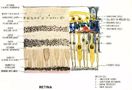
A diagram of retina is shown in figure1.1. The retina is made of many layers of
different cells. The cones and rods form the photoreceptor layer. These cells convert the optical information to the electrical signal. The final signals are passed to the ganglion
cells, which forms the optical nerves. Middle layers process the signal, compressing the information from approximately 100 million cells to 1 million cells.
Figure 1.1: A schematic diagram of retina
Required electric stimulus is a biphasic current pulse of variable durations as shown
in figure 1.2. Though cathodic leading pulses are preferred the circuit should also be able to deliver anodic leading pulses. Each pulse width is up to 1 ms. Main reason for using
path to ground, which may not be desired or feasible. Any net charge also leads to corrosion of electrode in saline fluid environment present in the eye and may limit the
long-term usage of implant. From the initial studies, 10 kΩ resistive load is determined
for the stimulator. It should be pointed out that the experiments have shown that the
stimulus and the load are variable and depend upon the retinal degradation and the position of the excitation at the retina. The load is also found not to be purely resistive
and can be modeled as a capacitor connected in parallel to the resistor. To achieve flicker free vision stimulus is required to have refresh rate of at least 50-60 Hz.
Figure 1.2: Required Biphasic pulse
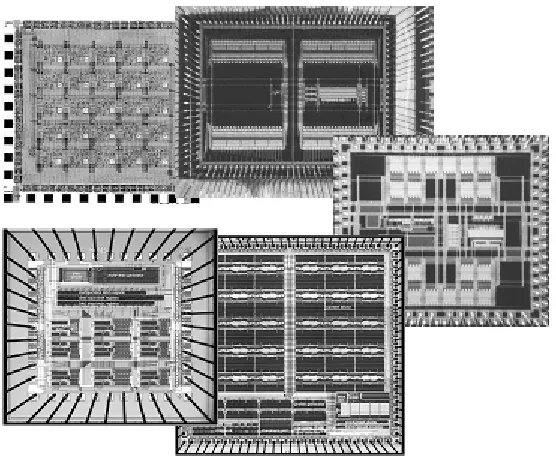
Retinal prosthesis group at NC state university has developed several generations
of Multiple Artificial Retinal Chipset (MARC), shown in figure 1.3. First chip, Retina-1
had 5x5 photo sensor array and current drivers and was fabricated in 2.0 µm technology.
From this chip, it was concluded that the photo sensor array on the implanted chip is not a
viable solution. Variation in the intensity of the light makes the design complex and hence increasing the chip size. Such sensing circuits also require large power. So the photo sensing circuits were shifted outside the eye and data link was established. Retina-2
demultiplexing. It had current scalability with 200, 400 and 600 µA full scale currents. It
had single rail supply voltage and a single current source with a bridge circuit providing both cathodic and anodic currents. Retina-3 chip had additional circuit for data recovery from a data link. An ASK demodulator and DLL was used for alternate PWM data
recovery. This chip was fabricated in AMI 1.2 µm technology.
Figure 1.3: Evolution of the chips, Retina-1, 2, 3, 3.55, 4 (clockwise from top left)
Recently developed Retina-3.5, Retina-3.55, Retina-4 chips have been fabricated in
AMI 1.2 µm process [11]. All chips have similar output driver design with changes in the
DAC structure and digital circuits. Retina-3.5/3.55 chips have 60 un-multiplexed driver
output. The chip area is 4.6 mm X 4.7 mm. A 4-bit DAC is used to deliver a current up to
600 µA. This current is amplified 10 times to achieve full-scale output current of 600 µA.
Wide swing current mirror is used for its low headroom requirement. Data is serially
and checksum. First the configuration data is used to set the timing and other parameters. The continuous data is distributed to the drivers for each frame. In Retina-4 amplification factor is increased from 10 to 30 to attain lower power. A single DAC is used so that the
there is better matching between anodic and anodic pulse. A multi-bias low-area 8 bits DAC was incorporated in the chip.
Initial studies have concluded that a 32x32 pixels (=1024) stimulus will provide face recognition. So the objective of this research is to increase the number of output channels in the stimulus chip to 1000. Initial estimations showed that the use of previous driver
design would not meet the power and area goals. So areas for improvements have to be identified and circuit modifications should be made. New functionality should be added
to enhance the usefulness of the chip. The resolution of the stimulus is increased from 4 bits to 6 bits or equivalently from 16 levels to 64 levels.
This report is presentation of ideas, simulations, circuit design and measurements
on the test circuit to achieve the goal. In the chapter two, the circuit analysis is done and circuit improvements are suggested. In this chapter, the calculations and simulated results are presented. A test chip is planned to test the circuit design and the design is presented
in chapter three. Chapter three also documents the circuit layout design. Measurement setup and results of the test chip are presented in chapter four. Chapter five concludes
Chapter 2
Circuit Design
2.1 Advance Fabrication process
Limited size of eye imposes a stringent condition on the size of the chip. Our aim is to limit IC size to 5 mm x 5 mm as determined by the medical specifications. An
extrapolation of area from previous chip showed that the design in AMI 1.6 µm process would not meet the criterion. Advance technologies with smaller feature size are evaluated for design. Estimation of the size for TSMC 0.35 µm technology is found to
meet the criterion. This estimated is verified by layout as will be shown in section 3.3. Feature size of TSMC 0.35 µm process is 4 times smaller than feature size of AMI 1.6 µm process. The reduction in the feature size reduces area of digital circuits by 16 (4x4)
times. Moreover, TSMC 0.35 µm has 4 metal layers compare to the 2 metal layers available in AMI 1.6 µm. Higher circuit densities can be achieved with more metal layer
as local and global routing takes considerable less area. It is pointed out that
approximately half of the area in the previous designs, in AMI 1.6 µm, was taken by
routing. It is estimated that to have 1000 outputs with the given chip size will require area
2.2 High voltage operations
High output stage power supply requirement is the main problem associated with
using the advance process technologies. TSMC 0.35 µm technology supports two power supply levels. Typical power supply is 3.3 V with minimal device drawn length of 400
nm. 5 V devices using second poly layers are also available. To support higher voltage HV devices have thicker oxide and increased minimal drawn length of 600 nm.
To overcome this problem, use of modified high voltage devices has been
suggested in the previous work [11]. These devices can be fabricated by simple modification in layout [12]. The basic principle of operation is to provide low-doped
region around the drain to reduce the maximum electric field. Channel implant layer and/or wells below the thick oxide layer are used to obtain low-doped region. These devices are reported to operate well in 10’s of volts for 5 V standard process and have
been demonstrated in number of standard process technologies. It should be noted though the Vds can be high, maximum Vgs is limited due to same thickness of thin oxide. After
careful analysis these devices are found to be unsuitable for our application due to big size, high series resistance, and poor matching.
The circuit is designed to operate at ±6.5 V. It was noticed that a circuit could be
designed such that the maximum voltage on the devices is limited to 6.5 V. In this circuit, use of 5 V devices at 6.5 V is justified in section 2.3.
2.2.1 Output stage
If typical NMOS/PMOS output stage is used maximum voltage appearing on the
M2 at 12.5 V. This problem can be alleviated with protecting transistors M3, M4 as shown in figure 2.1(ii). In this circuit, additional transistor M3 and M4 have gate connected to gnd, so 12.5 V drops across two transistors. Vds for M4, and M2 is
6.0+|Vthp|, and 6.5-|Vthp| respectively.
-6 .0
M 1 M 2 + 6 .5
- 6 .5 + 6 .5
V o n
- 6 . 0
M 1 M 2 + 6 . 5
- 6 . 5 + 6 . 5
V o n 0 . 0
+ |V t h p |
M 3 M 4
Figure 2.1: (i) Typical output stage (ii) Output with protection transistor
2.2.2 Voltage level shift
The digital circuit is operating at 3.3 V with respect to the Vss supply rail. The
gnd can be achieved with circuit shown in figure 2.2. The second stage is not necessary if the output voltage swing to the gnd is not required.
o u t
D ig ita l_ in
V s s V d d
g n d b ia s
Figure 2.2: Digital output to driver circuit interface circuit
2.3 Reliability
As mentioned previously, the TSMC 0.35 µm process provides only 5 V devices
and use at 6.5 V has to be justified. As the stimulator has to be implanted inside the eye, which obviously may not be repeated often, the design should work reliably for at least a
decade. In our context reliability refers to the failure of the circuit. Increase in operating voltage causes stress resulting in time dependent device degradation. Oxide stress and hot carrier effect are two prominent effects that need to be considered [13]. Time dependent
2.3.1 Oxide stress
TDDB is results of the wear-out of the insulating properties of the gate oxide.
Most of the models for predicting the lifetime are based upon curve fitting. Thick oxide under high field stress usually follows the 1/E model given in equation 2.1.
∗ = OX BD t GE
t exp (2.1)
At 250 C reported values of t is1.0E-11 sec, and G is 350 MV/cm. Temperature effect are
taken into account by temperature dependent t and G with the following relationship:
− − ∗ = 300 1 1 exp ' T k E t t B
B (2.2)
− + = 300 1 1 1 0 T k G G B δ (2.3)
Thick oxide with moderate electric field follows the E model given in equation 2.4.
(
OX)
BD t E
t = 1∗exp −γ ∗ (2.4)
At 1250 C reported values of t1, and γ are 6.3x10¹⁴ sec, and 2.66 cm/MV respectively. The above values are obtained by curve fitting including thickness of at 15 nm. The temperature dependence can be accounted by equations 2.5 and 2.6.
∆ ∗ = T k H t t B
BD 10 exp 0 (2.5)
T c b+ =
γ (2.6)
Increasing the thickness of oxide results in lower oxide electrical field. For example the
oxide thickness is increased from 7.5 nm to 14.6 nm. For the typical value of thick oxide of 14.6 nm, the Eox is 4.45 MV/cm, which is approximately equal to oxide field in 3.3 V
devices. From the above equations, considering normal temperature and parameter
variations the predicted lifetime is over 60 years. In literature, acceptable value for reliable device performance is reported as 7 MV/cm [14]. This analysis is also supported
by lifetime measurement values reported in [15].
2.3.2 Hot carrier effects
It is well known that the hot-carrier induced device degradation is limiting factor for deep submicron device applications [16]. The hot carrier models are not available in
cadence simulator. There are no simple expressions to calculate device degradation for submicron devices. The exact modeling of the device lifetime is beyond the scope of this research. In this section, conclusions are drawn from published work.
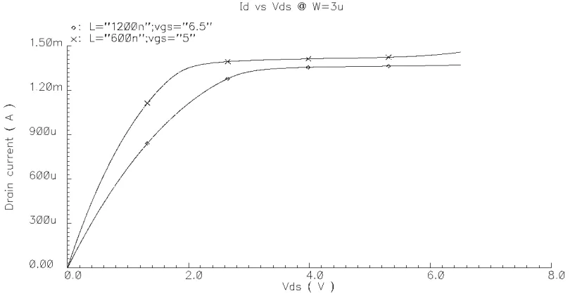
A way to reduce this high field in the channel is to increase the length of the devices [17]. For example in TSMC 0.35 µm devices, 3.3 V and 5 V devices have
minimum drawn length of 400 nm and 600 nm respectively. This increment of length is used to limit the maximum current and lower the electrical field. For this reason, all the devices subjected to 6.5 V have minimum drawn length of 1200 nm (2 x 600nm). PMOS
performs better than NMOS for hot carrier effect and analysis for NMOS is shown in this section. The increment of length limits the maximum current as shown in figure 2.3.
Hot carrier damage rate is highest in a NMOS when the drain-source voltage is the maximum permitted voltage while the gate-source voltage is around half of the drain-source voltage [13]. Device degradation due to hot carrier is measured by reduction in
n Ts m SUB m D s
it N W H I t I t dt
N • • • ∝ ∆
∫
− 01 ( ) ( )
1
(2.7)
Where Ns, Ts, ID, ISUB are number of transitions, time duration per transition,
drain current and substrate current respectively. H, n and m are degradation parameters determined by the experiments.
Figure 2.3: Drain current as a function of drain source voltage to compare devices The lifetime is determined assuming the worst-case scenarios in the circuit design. Actually the device is designed for ASIC purposes and is usually overkill for circuits. In
the circuit design, where spice level circuits are available, these conditions may be checked and prevented. The effect of degradation on the circuit is to be considered on the basis of the five factors [19]:
1. Hot-carrier degradation model precision and accuracy 2. The specific MOSFET terminal waveform
3. MOSFET switching activity
5. Relative importance of the degraded circuit paths
The circuit degradation is a linear function of the frequency of operation as shown in equation 2.7. While the process has been designed to operate at 100’s of MHz, in our
application where all transistors operating at higher voltage are required to work at relatively low frequency of a few kHz. Circuit sensitivity to the device degradation is
very less. Usually 5%-10% variations in device currents are used for design lifetime calculations. This circuit can tolerate 10’s of percentage of change in all 6.5 V devices. Moreover there are no critical paths in the design.
2.4 Power supply reduction
The circuit power consumption should be reduced to increase the number of drivers on the chip. Currently ±7 V power supply is being used. 7 V is required as the 600
µA of maximum current at the 10 kΩ load means 6 V of drop and circuit has 1 V
headroom to sustain proper operation. Reducing the power supply will reduce power dissipation of the circuit. Power supply voltage reduction is also desired for better device lifetime.
2.4.1 Matlab simulations
the driver is obtained when the output power is maximum. Since the overall power available to the implant may be limited this result is a desired feature.
Figure 2.4: Matlab simulation of the power supply variation for a driver
2.4.2 Alternative output circuit
In the driver circuit the output stage is a wide swing current mirror stage. The
headroom requirement for a wide swing circuit is: Vheadroom=2∗Vov+2∗Vmargin.
Where Vov is the overdrive voltage (Vgs – Vth) of a transistor and Vmargin is the excess voltage required for guaranteed saturation operation of the transistor. The first step towards the solution is to realize that the current is mirrored by bottom most transistor in
the stack and other transistor(s) is(are) used to increase the output impedance of the driver. Active feedback current mirror circuits that work at lower headroom are reported
For this circuit, as shown in figure 2.5, the headroom voltage requirement will be:
Vres in Vm Vov
Vheadroom= + arg + . The Vres is the voltage required by the stacked
transistors operating in linear region, which is in the range of 50-100mV. The Vmargin is chosen to be 50 mV and the Vov is 350mV and hence headroom voltage is reduced to 500
mV. A further reduction in Vov can be obtained but with some penalties. Reduction in overdrive voltage makes the circuit more vulnerable to the Vth variations. Specially, at the lower range of operation the effect will be more prominent due to the lower Vgs.For
example with 6-bit resolution minimum Vov is equal to 44.1 mV
(
350mV∗ 63)
. Also toreduce overdrive voltage, width of the transistors has to be increased, which will result in bigger driver size.
_ +
D A C
M 1 M 2 M 3 M 4 gnd V ss vbias O utput M 5
Figure 2.5: Output stage with op-amp feedback circuit
In this circuit the transistor M5 is used as a protective device. For output up to
|Vth|, all stacked transistor (M1, M3, M5) are in saturation region. For output below -|Vth| M5 enters in linear region. To provide near maximum voltage, M3 can not remain in the saturation region and also enters the linear region. For this range the op-amp output
transistor except during the maximum current output, M3 and M5 remain in saturation region and hence circuit has very high output impedance. Though only NMOS side is shown for cathodic output, similar PMOS structure exists to provide anodic output.
2.4.3 Op-amp design
To determine op-amp requirements a circuit with an ideal op-amp is simulated. Results, shown in figure 2.6, indicate that the gain of the op-amp is not important for the lower 90% of the range as the stacked transistors operating in the saturation region
provide sufficient output impedance.
Figure 2.6: Current mirror ratio as a function of op-amp gains and offsets
At higher current output, shown in figure 2.7, a minimum gain is required to suppress the effect of offset and to maintain minimum output impedance. The figure
plotted for ±20 mV offset shows that a gain of 70-80 would be sufficient to obtain a good
Figure 2.7: Current mirror ratio for large currents as a function of op-amp gains and offsets
For this specific design op-amps also have to meet following requirements. The op-amp should consume small power. If the power requirement is big than the incentive
to use op-amp will be lost. Secondly, the circuit should be small as it is associated with every driver and will be repeated as many times. Thirdly, the circuit has to operate for input very close to the one side of the supply rail. Fourthly, the output of the op-amp
should be able to swing to the ground rail. Finally, the op-amp in the feedback loop should be stable.
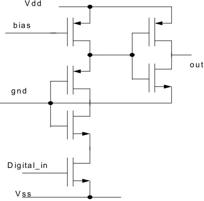
To meet all above requirement a two stage circuit is employed as shown in the figure 2.8. This circuit is modified from the circuit presented in [20]. The modification is required as the load capacitance to the op-amp is bigger in the present application leading
achieved through the second stage. It should be noticed that the transistor design is not
in + in - output
vss gnd
M1 M2
M3 M4
M5 M6
opam p bias
Figure 2.8: Cathodic current mirror op-amp
symmetric and hence the transistors should be sized carefully to achieve to minimized systematic offset. All the transistors have to be few times of minimum size so that the process variation can be reduced. Though the circuit would tolerate moderate offset as
shown previously.
Similarly anodic op-amp is also designed where the NMOS and PMOS devices
are interchanged. Stability and gain of the amplifiers is the main criterion of the design. Any op-amp used with feedback has to be stable so that the oscillation can be prevented. Frequency response of cathodic and anodic op-amps is plotted in figure 2.9 and 2.10.
Figure 2.9: Frequency response of cathodic op-amp
Figure 2.10: Frequency response of anodic op-amp
Figure 2.11: Current amplification for cathodic stimulus
Figure 2.12: Current amplification for anodic stimulus 2.5 DeMultiplexing
cathodic pulses is 1 ms each. Effectively any output is ‘on’ for 2 ms for each time period. So it is concluded that a driver can be demultiplexed to provide stimulation at 8 outputs.
Use of transmission gate is a standard method to demultiplex current output.
Current demultiplexing with transmission gates causes problems in this circuit. To pass
600 µA of current with small voltage drop would require large transmission gate. The
output voltage is of the driver is up to ±6 V, so source-gate/drain-gate voltages of
transmission gate transistors would be up to 12 V. Transistors designed for 5 V supply
can not be used at such high voltages.
The solution lies in the integration of the demultiplexing with the output stage of
the driver. The resulting circuit is shown in the figure 2.13. In this circuit, M1 forms a current mirror with M2 to amplify the DAC current 30 times. M5, M7,….M19, with gate connected to the gnd are protective transistors as explained earlier. The middle transistors
in the stack, M3, M6,…., M18, are used to switch ‘on/off’ the demultiplexed output. Gates of these transistors are connected to Vss to switch ‘off’ and to output of the op-amp to switch ‘on’.
Simulation result of demultiplexing circuits is shown in figure 2.14. In figure 2.14(a), the digital control signal of output 1 and output 5 are displayed. In figure 2.14(b),
+
DAC
M1 M2
M4 gnd
Vss vbias
_
M3 Output 1 M5
M6 Output 2 M7
M18 Output 8 M19
Figure 2.13: De-multiplexed output stage
(a) Outputs (b) Control Input
2.6 Variable supply voltage
One of the problems faced in the design is an inaccurate model of load presented
to the circuit from the retina. The problem is that without implant correct tissue impedance can not be found and without precise impedance values an optimal implant
circuit can not be designed. 10 kΩ impedance is reported in single electrode experiments.
Actually, the tissue impedance as well as the maximum current requirement may vary. If the actual requirements are over the designed values, the circuit will not be able to deliver
that. On the other hand if the actual values are smaller than estimated, the circuit will be wasting a large amount of power in the driver circuit. In this section, analysis of these variations on circuit performance is presented. Circuits capable of operating at variable
supply are shown to be efficient.
2.6.1 Matlab simulations
In matlab simulations chip power refers to the power of the output stage of the driver. This assumption is justified due to large power consumption in the output stage
compared to the full circuit. It is noticed that any reduction in Vdd (Vss = -Vdd)will also reduce power in other circuits. Power in digital circuit is not affected by output power
requirements. In these simulations, the output power Pload =Iout2×Rload
, total power
out dd total V I
P = × and chip power Pchip =Ptotal −Pload.
2.6.1.1 Current variations
In figure 2.15, the power curves for various Vdd and 10 KΩ load are plotted. The load power is independent of the supply voltage. If the maximum current required for
as shown by the chip power curves. The power reduction is due to decrease in unnecessary voltage drop
Figure 2.15: Power curves for variable supply
across the output driver stage. Proposed reduction of Vdd up to 3.5 V can reduce power consumption of the total power and output driver stage power up to 46.1% and 85.7%
respectively.
2.6.1.2 Load variations
Any reduction of load will results in linear reduction in the load power. Due to constant Vdd total power of the circuit is not reduced. This implies that the chip power is increased significantly. In the figure 2.16, the power curves for 5 KΩ resistant (half of the
specified load) are plotted for Vdd values of 6.5 V and 3.5 V. Increases in chip power at 6.5 V should be noticed. If the Vdd is reduced to 3.5 V, the total power and output stage
Figure 2.16: Power curves for variable power supply at reduce load
2.6.1.3 Multiple power supply chip
The chip may be stimulating different part of the retina. It has been reported that
the part of retina close to fovea requires less stimulation. A power efficient chip will require multiple Vdd so that driver operation can be optimize to variable load resistance
and maximum current requirements. It is recognized that the providing multiple power supply will have a cost in term of area on the chip as well at the power supply circuit. An analysis was done to find the power savings, which could be used in such cost benefit
analysis.
A model is constructed for 1000 output chip to predict the power savings. We
figure 2.17. Area I, II, III are formed with three concentric circles and area IV is the difference between the square and the largest circle.
1 un
it
0.8 un
it
0.
6 un
it
Area I Area II
Area III Area IV
Figure 2.17: Regions for variable stimulus
The center of theses circle is at the point of least required stimulus and hence 3.5 V power supply is used. Area II, III and IV progressively far and are supplied with 4.5,
5.5 and 6.5 V supplies respectively. The number of drivers associated with each supply is proportional to the area associated with it for a constant density of electrodes. For this
model 283, 220, 283, and 214 outputs are found in area I to IV respectively.
Maximum stimulus current of 300 µA, 400 µA, 500 µA and 600 µA can be provided in area I-IV respectively. Fixed 10 KΩ load resistance is assumed in all regions.
One set of simulations is done under maximum current condition to find out maximum power savings. Simulations for uniformly distributed currents are done to find typical
savings of approximately 20% and maximum chip power saving of 72.1% can be expected.
Table 2.1: Simulated power for variable supply voltage
Fixed supply voltage (mW)
Variable supply voltage (mW)
Power saving (%) Output
Currents Total power Chip power Total power Chip power Total Power Chip Power
Maximum 359.8 99.2 288.2 27.7 19.9 72.1
Uniformly distributed
185.9 93.9 149.3 57.0 19.7 39.1
2.6.2 Circuit and simulations
The designed circuit was changed to accommodate the power supply variation. Care is taken especially to set bias point with respect to correct power supplies. The
circuit can be operated from ±6.5 V to ± 3.5 V with lower margin of 0.1 V. Any further
reduction may not be tolerated as it affect the op-amp operation which has three stacked transistor operating in saturation region. Output at various Vdd is shown in figure 2.18.
Figure 2.18: Output for variable power supply
2.7 Variable Output
As stated previously, the circuit may not require high current. Present studies
conclude that the maximum current may be as low as 30 µA. In such case required
resolution can not be provided with high amplification factor. For example, 9.52 µA of resolution is provided with 6-bit DAC when maximum current is 600 µA. This is
illustrated in figure 2.19, where curve A and curve B represent 600 µA and 300 µA maximum current respectively. For a driver with 200 µA of maximum current
requirement curve A has 21 level resolution while curve B has 42 level resolution.
In the previous IC design, variation in the amplification was achieved through change in bias current in bias generation circuit. The bias current values of 10, 20 and 30
designed for maximum bias current and reduction in bias current results in lower overdrive voltage and poor matching. Secondly, bias current may not be reduced to very small value due to problem in generating accurate small currents and biasing with low
currents. This means that maximum output current can not be reduced arbitrarily. Thirdly, bias circuit is a global circuit and individual driver can not be programmed.
D A C I n p u t
1 0 2 0 3 0 4 0 5 0 6 0 6 3
1 0 0 2 0 0 3 0 0 4 0 0 5 0 0 6 0 0
0 0 St im ul at or Ou tp ut ( u A )
C u r v e A
C u r v e B
Figure 2.19: Variable amplification illustration
A different approach is proposed in the circuit shown in figure 2.20. In this
circuit, current mirror amplification factor changed by selecting fewer output stage mirror transistors. Maximum current may be selected from 20 µA to 600µA in steps of 20 µA. This selection range can be fully or partially hardwired and/or made programmable.
While it is possible to make the fully programmable, doing so requires overhead circuit in terms of implementing the switches and control circuits. The best solution will be to
amplification factors of 6 and 30, corresponding to the maximum output current of 120 µA and 600 µA respectively, are chosen. Simulation results are shown in figure 2.21.
_ +
M1 M32
M31
Vss
Mi Mj M30
M33
Figure 2.20: Variable amplification circuit
Figure 2.21: Variable amplification simulation
programmability will be very beneficial. Area of the circuit could also be reduced when the ratios are hardwired and unused mirrors are removed. Power dissipation of this approach is more than previous approach. This increase is due to the fact that the current
of the stages other than the output stage is not reduced. But the increase is mostly insignificant part of overall power. It is significant only when the overall power is small,
hence performance is not affected.
2.8 Maintaining charge neutrality
The circuit is designed to output charge balanced biphasic pluses. It is noticed that the final output may not be a fully charge balanced. The process deviation will affect the
current mirror matching leading to a mismatch in the anodic/cathodic pulses. Other unintended sources may also make a small finite build up of charges. The chronic effect of the charge build up is unacceptable. Hence an effective means for charge removal
should be presented.
The desired element for charge removal is a switch-activated resistor connected to
the gnd. An optimal value of resistor has to be decided by two conflicting requirements. Small resistance will induce large discharge current in the circuit. Large resistance will require more discharge time.
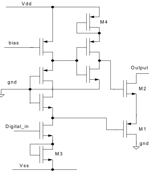
The previous design used a PMOS transistor connected between output and gnd to remove the charge from the output. The PMOS gate is switched to the Vdd to during ‘off’
state and connected to Vss during ‘on’ state. A problem with the circuit is that during PMOS ‘off’ state and output being low the voltage difference between the gate and drain voltage is 12.5 V, way more than allowed. Secondly, the transistor works as a resistance
A new circuit, shown in figure 2.22, has been proposed. A PMOS, M1 and a NMOS, M2 is connected in series to form a path to gnd from the output. A benefit of series connected PMOS and NMOS is that at high output voltages one of the transistors
works as current source to limit the current irrespective of the charge polarity. Sizing of PMOS and NMOS can be adjusted to fix maximum positive and negative currents.
Maximum current and resistance can be adjusted with sizing and applied gate voltages.
D ig ita l_ in
V s s V d d
g n d b ia s
O u tp u t
g n d M 4
M 1 M 2
M 3
Figure 2.22: Charge cancellation circuit
Gates of M1 and M2 are controlled using modified level shifting circuit. M3 and
gate to source/drain voltage. To reduce the maximum current, more such diode connected transistors can be added to further reduce the applied gate voltage.
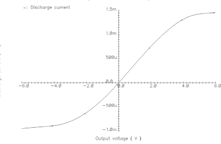
Simulations of the circuits are presented in the figure 2.23 showing the discharge
current with respect to the output voltage. Straight-line response close to the origin shows 3 KΩ discharge resistance. Maximum anodic and cathodic currents are 1.5 mA and 1.0
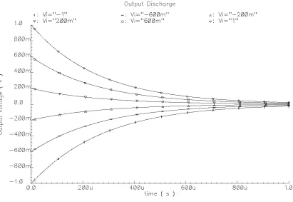
mA respectively. Figure 2.24 shows the transient behavior for small output voltages for both polarities. A 100 nF capacitor is added to the output for this simulation.
Figure 2.24: Charge cancellation transient response
2.9 DAC
Binary DAC and multi-bias DAC are two main types of DAC topologies. In binary DAC all transistor gates are biased at same potentials and the width of transistors are varied in the powers of two. Multi-bias DAC has all transistors of same size and gate
voltage of transistor is varied. Binary DAC has better integral non-linearity (INL) and dynamic non-linearity (DNL) than multi-bias DAC but requires more area. In binary
DAC the active device area increases by a factor of two for each additional bit.
In the stimulus chip, DAC is a dedicated part of a driver and hence will be replicated 125 times in a 1000 output chip. So small area DAC is very much desired. A
between transistors in DAC bias circuit and DAC. Biases, used in DAC, are generated in one central bias circuit and are distributed throughout the chip. Mismatches in distant transistors will be considerable compare to proximity transistors. There are many reasons
for mismatch for example W/L, mobility, and Vth variations.
If 6-bit binary DAC is used, for reasonable size of transistors the bias voltage will
be very small. Such bias voltage will enhance problems due to Vth variations. Secondly, size of this DAC will be much bigger. If 6-bit multi-bias DAC is used, six bias voltages will be required resulting in more routing area. Multi-bias DAC also has more DNL
problem compared to binary DAC.
It is noticed that in this application DNL is more important compared to INL or in
other words output should be monotonic. INL mismatch results in having a same output on two different pixels for the same input. DNL mismatch can result in having a same output for two different inputs for same driver. Drivers located close to each other will
have similar INL and hence will be less problematic. The problem found in both above-mentioned architectures is attributed to use of binary codes and can be alleviated by using thermal codes [23]. Using a full thermal coded DAC will result in unacceptably big DAC.
A new DAC designed with above-mentioned considerations is shown in figure 2.25. In this circuit, 2 most significant bits (MSBs) are implemented with thermal codes.
4 LSBs are implemented as binary coded conventional binary DAC circuits. Separate biases for these circuits are used. DAC bias circuit is shown in figure 2.26. Highest possible bias potentials are used. Bias values are limited by lower limit of Vdd (=3.5 V).
W/L gnd Binary_Bias Thermo_Bias 2*W/L 4*W/L 8*W/L W2/L2 gnd DAC Output Cascode_Bias W/L 2*W/L 4*W/L 8*W/L W2/L2 W2/L2 W3/L3 W3/L3 W3/L3
Figure 2.25: DAC circuit
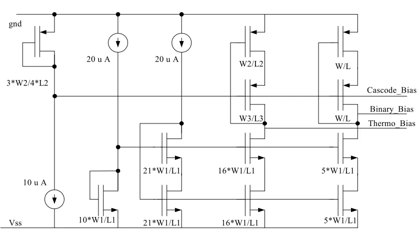
gnd Binary_Bias Thermo_Bias W/L W2/L2 3*W2/4*L2 Vss W/L W3/L3 16*W1/L1 16*W1/L1 5*W1/L1 21*W1/L1 21*W1/L1 10*W1/L1 5*W1/L1
20 u A 20 u A
10 u A
Cascode_Bias
Table 2.2: Transistor sizes for DAC circuit
Transistor size Value (µm)
L 3.6 L1 4.8 L2 4.8 L3 3.6 W 1.8 W1 1.8 W2 1.8 W3 3.6
2.9.1 DAC performance
Maximum DAC current at power supply values from 3.5 V to 6.5 V is shown in
figure 2.27. Overall current variation is less than 0.25% or 0.15 LSB. Figure 2.28 shows the transient response of circuit in staircase format. The spikes are present due to absence
of significant capacitance at the output. Figure 2.29 shows INL, DNL and absolute accuracy of the DAC. All of these parameters are found to be within 0.16 LSB.
2.10 The stimulus circuit
The resulting circuit is shown in the figure. 2.30. A 6-bit DAC produces current
up to 20 µA determined by the pixel intensity of the image. DAC output is amplified with current mirrors of ratios up to 30 to provide maximum current of 600 µA. Variable
current mirror ratios are used to maintain resolution for lower stimulus requirement. The current mirror is implemented with active feedback so that the voltage headroom can be reduced to 0.5 V while maintaining output resistance. The mirror output is demultiplexed
Figure 2.27: Power supply variation effect on the DAC
Figure 2.29: INL, DNL and absolute variation of the DAC
The switches are implemented with single NMOS or PMOS transistor based upon the voltage levels. For anodic output, the DAC current is reflected to the Vdd rail using 1:1
current mirror and similar circuit using complementary devices is used.
Demux & discharge
8 output8
DAC Current mirror
(with feedback op-amps and variable ratios) Demux & discharge 1 Switches output 1 …. Digital input Demux & discharge
8 output8
DAC Current mirror
(with feedback op-amps and variable ratios) Demux & discharge 1 Switches output 1 …. Digital input
Chapter 3
A Test Chip and Circuit Layout
3.1 Test chip objective
As stated before a chip is to be fabricated in TSMC 0.35 µm technology. The chip
will not only contain the circuit described in the previous chapter but also bias and digital circuit. The digital circuit will mainly consist of the data acquisition and transfer, timing profile generation, and control units. A central bias circuit will be required to generate
reference current. A test chip was planned in AMI 1.6 µm process technology to demonstrate and debug the driver circuit. Careful planning is required to demonstrate the
functionality and to draw inferences for TSMC 0.35 µm design. Test chip circuit is designed as discussed in the previous chapter but does not include DAC. The design was sent to MOSIS for fabrication.
3.2 Test chip design
The AMI 1.6 µm process technology is different from TSMC 0.35 µm process technology in many aspects. Usually a design can be scaled by the lambda rule. However lambda scaling may not be done in this case due to separate lambda rules for AMI 1.6 µm
(SCMOS) and TSMC 0.35 µm (SCMOS sub-micron). TSMC 0.35 µm allows stacked vias, which AMI 1.6 µm does not allow. The scaling is also not possible as the process
3.3 Circuit layout
To put 1000 outputs on the chip requires not only better design but also dense layout. Layout rules are followed diligently in the layout to achieve dense circuit. TSMC
0.35 µm design layout was completed to verify our initial claims of achieving 1000
output in 5 mm x 5 mm chip. The layout of a driver with 8 outputs is shown in figure 3.1. The size of this layout is 92 µm x 525 µm and 125 driver circuits will take 6.04 mm2.
Which is just 25 % of the chip area. Assuming equal digital area (as approximately in previous chips), it can be concluded that the area goal can be achieved. It is noticed that the routing area may not be significant as metal layer 3 and 4 can be used for routing.
Figure 3.1: Driver layout in TSMC 0.35 µm process
3.3.1 Matching
Matching between transistors is considered in current mirrors and op-amp circuits. Capacitive matching (symmetric circuit topology) is not required as operational
example, the reference current is mirrored to generate bias voltages for DACs, DAC uses a mirror stage and the DAC current is mirrored to the final output stage. Also op-amps require good matching to minimize offset.
The ground rules to obtain good matching are followed [24]. Some of the highlights of the circuit layout are the same orientations, proximities, same environment,
and bigger size. A circuit layout of the output stage current mirror is shown in figure 3.2. Bottom and top rows are of NMOS and PMOS respectively. For current mirrors, input transistors M1 and M3 are located in the middle of the row to follow the common
centroid approach. Transistor M2 is used to reflect the DAC current to the PMOS row as only one DAC is used in design. Proximity of M1 and M2 is important to the design. All
transistors are oriented in the same direction and have similar environment.
3.3.2 Test chip layout
The test chip layout is shown in figure 3.3. The chip has two drivers, a bias circuit
and few test structures. In one of the drivers, probe pads are connected to the output of the main blocks. These probe pads would have been helpful in debugging the circuit in
case of any malfunction. A NMOS, a PMOS and both type of op-amps are placed as test
devices. Two external 20 µA current sources are used as reference in the bias generation
circuit.
Chapter 4
Measurements and Results
4.1 Testing setup
A microphotograph of the fabricated test chip is shown in figure 4.1. A breadboard
test setup is designed as shown in figure 4.2. Use of breadboard in place of PCB is
justified, as the frequency of operation of the circuit is very low. 20 µA bias current for
anodic and cathodic circuits are achieved using fixed and variable resistances. 5 KΩ load resistors of 1% accuracy are used for current bias measurement. The switching inputs
1 2 3 4 5 6 7 8 9 10 11 12 13 14 15 16 17 18 19 20 40 39 38 37 36 35 34 33 32 31 30 29 28 27 26 25 24 23 22 21 10 Kohm 10 Kohm 10 Kohm 10 Kohm 10 Kohm 10 Kohm 10 Kohm 10 Kohm 10 Kohm 10 Kohm 10 Kohm 10 Kohm 10 Kohm 10 Kohm 10 Kohm 10 Kohm HP 4142B 10 Kohm 100 pF 10 Kohm 100 pF 10 Kohm 100 pF 10 Kohm 100 pF 10 Kohm 100 pF 10 Kohm 100 pF 10 Kohm 100 pF 10 Kohm 100 pF 10 Kohm 100 pF 10 Kohm 100 pF 10 Kohm 100 pF 10 Kohm 100 pF 150 Kohm 1.5 Mohm Vdd Vdd Vdd First driver output 1 input output 2 output 3 output 4 output 5 output 6 output 7 output 8 Second driver output 1 output 2 output 3
output 4 output 5 output 6 output 7 output 8 input Vdd floating anodic circuit bias cathodic circuit bias Vss gnd anodic switch cathodic switch amplification selection switch charge cancellation switch Vss Vss Demux 1 switch Demux 2 switch Demux 3 switch Demux 4 switch Demux 5 switch Demux 6 switch Demux 7 switch Demux 8 switch 100 Kohm 150 Kohm 100 Kohm
Figure 4.2: Measurement setup
are sensitive to high voltage that may be induced due to transients. The sensitivity is due to the high impedance and low breakdown voltage of gate. So these pins are connected
full-scale current of 20 µA is generated through HP 4142B instrument. The output is also
measured through this equipment. The ‘C program’ used in the instrument is attached in appendix A.1.
4.2 Measurements
4.2.1 Power supply reduction
The circuit is designed to operate at lower power supply of ±6.5 V in place of ±7 V. The anodic and cathodic response of the circuit is plotted in figure 4.3. The drop of the current
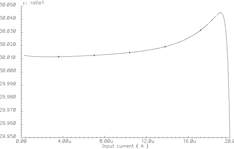
toward the end of the range is due to limited gain of the op-amp. This problem will be alleviated in TSMC 0.35 µm process due to higher one stage gain. The output current to input current ratios are shown in figure 4.4. The effect of Vth variation is evident at the
lower range. The ratio variation is within 1% for cathodic current and 2% for the anodic current.
Figure 4.4: Output current and input current ratios for fullscale current of 600 µA
4.2.2 Anodic/Cathodic waveforms
Figure 4.5 and 4.6 show anodic and cathodic pulse leading voltage waveform at ±6.5 V supply voltage respectively. The frequency of operation is 60 Hz. The load for these plots is 10 KΩ and in the plot the voltage across the load is displayed. The rise and
fall times of the wave are sharp due to absence of external capacitive load.
Figure 4.6: Anodic pulse leading output waveform
4.2.3 Demultiplexing
Figure 4.7 shows the output waveforms of two demultiplexed outputs of a driver circuit. The frequency is adjusted at 60 Hz and the pulse width is 2 ms. The DC level has been shifted to show the waveforms clearly.
4.2.4 Variable supply voltage
The figure 4.8 shows the output at the reduced power supply. Flattening of the
curve is seen as the output reaches power supply rail and further current can not be sustained.
Figure 4.8: Output with ±3.5 V supply
4.2.5 Variable amplification factor
Output for reduced amplification factor of 6 can be seen in figure 4.9.
Amplification factor of 6 corresponds to maximum output current of 120 µA. The output
current to input current ratio is shown in figure 4.10. The effect of Vth variation is evident at the lower range. The ratio variation is within 0.8% for cathodic current and 3% for the
Figure 4.9: Output current for amplification factor of 6
Figure 4.10: Output current and input current ratios for fullscale current of 120 µA
4.2.6 Charge cancellation
Charge cancellation mechanism is desired to remove accumulation of charge. To
Figure 4.11 shows the anodic output waveform in the absence of charge cancellation. The time constant of this output load is τ = RC = 4 ms. Output discharge time is visible in that range. When the charge cancellation mechanism is applied the discharge of the output is
much faster as shown in the figure 4.12. From this measurement, approximated resistance of the charge cancellation circuit is 3 kΩ.
Figure 4.11: Output waveform in the absence of charge cancellation
4.2.7 Matching
Output stage anodic/cathodic current matching is one of the important aspects of this design. Matching is result of the manufacturing variations and is statistical in nature. Since 5 chips with two drivers each were fabricated, we have 10 drivers to find statistical
Figure 4.12: Output waveform with charge cancellation
Chapter 5
Conclusion
5.1 Conclusion
Driver is an important part of retinal prosthesis project. From power perspective, it
is the most critical block consuming most of the power budget. The analysis presented in this thesis is not only limited to the present work but also to the general driver design. The analysis results are obtained through matlab simulations. Circuits with new
topologies and application of previous works are presented. Circuit simulation results are shown and analyzed. A test chip has been fabricated to demonstrate the circuit feasibility. Measurement results are presented and found to be as expected.
5.2 Future work
Some suggestions for future work are listed in this section. Though the driver design has been completed, digital circuit and bias circuit has to be incorporated in the
chip. The chip data is serially acquired, checked and distributed to the driver. In the previous design data was serially pushed to each driver. As the number of driver increases, a global bus for data transfer to the drivers may be a good approach. Or several
drivers may be clustered and data would be serially supplied to each cluster.
Arbitrary waveform generation can be achieved by some circuit modification. In
output constantly ‘on’. The digital controller circuit needs to be modified from previous designs to incorporate demultiplexing and additional bits for the DAC. Bias generation circuit has to be modified to operate from 3.5 V to 6.5 V. Multiple supply may be
References
[1] J. Kirk, “Machines in our hearts: the cardiac pacemaker, the implantable defibrillator, and American Healthcare,” John Hopkins University Press, 2001.
[2] F.A. Spelman, “The past, present and future of cochlear prostheses,” IEEE Engineering in medicine and biology magzine. Page 27-33 may-june 1999.
[3] “The bionic man: Restoring Mobility,” Science, vol. 295, 8th February 2002. [4] Website: http://www.bioen.utah.edu/faculty/RAN/index.html.
[5] Website: http://www.dice.ucl.ac.be/Mivip/.
[6] Website: http://134.2.120.19/index_en.html [7] Website: http://www.optobionics.com.
[8] Website: http://rleweb.mit.edu/retinaold/.
[9] Website: http://www.cmplx.cse.nagoya-u.ac.jp/research/retina/.
[10] M. S. Humayun, E. de Juan Jr., J. D. Weiland, G. Dagnelie, S. Katona, R. Greenberg, and S. Suzuki, “Pattern electrical stimulation of human retina,” Vision research, vol. 39, pp. 2569-2576, 1999.
[11] S. C. DeMarco, “The architecture, design, and electromagnetic/thermal modeling of a retinal prostheses to benefit the profoundly blind,” PhD thesis, NC state university, to be published.
[12] C. Bassin, H. Ballan, and M. Declercq, “High Voltage devices for 0.5 µm standard CMOS Technology,” IEEE Electron Device Letters, vol. 21, January 2000.
[13] MOSIS Inc. Reliability in CMOS IC design: Physical Failure Mechanism and their modeling. [Online]. Available: http://www.mosis.org/Faqs/tech_cmos_rel.pdf.
[14] R. Moazzami and C. Hu, “Projecting gate oxide reliability and optimizing reliability screens,” IEEE Trans. Electron Devices, vol. 37, pp. 1643-1650, July 1990.
[16] S. H. Renn, J. L. Pelloie and F. Balestra, “On the determination of the time-dependent degradation laws in deep submicron SOI MOSFETs,” European Solid-State Device Research Conference, September 1997.
[17] Y. Tsividis, “Operation and modeling of the MOS transistor,” 2nd edition, McGraw-Hill, 1999, pp. 286-290.
[18] K. N. Quader, P. K. Ko, C. Hu, P. Feng, and J. T. Yue, “Simulation of CMOS circuit degradation due to hot -carrier effects,” International Reliability Physics Symposium, 1992.
[19] W. Jiang, H. Le, J. Chung, T. Kopley, P. Marcoux and C. Dai, “Assessing circuit-level hot-carrier reliability,” International Reliability Physics Symposium, 1998.
[20] D. Schmitt, and T. S. Fiez, “A Low voltage CMOS current source,” International Symposium on Low Power Electronics and Design, pp. 110-113, Aug. 1997.
[21] J. R. Ramirez-Angulo, R. G. Carvajal and A. Torralba, “Low supply voltage high-performance CMOS current mirror with low input and output voltage requirements,”
IEEE Midwest Symposium on Circuits and Systems, pp. 510-513, Aug. 2000.
[22] S. C. DeMarco, W. Liu, P. R. Singh, G. Lazzi, M. S. Humayun, and J. D. Weiland, “An arbitrary waveform stimulus circuit for visual prostheses using a low area multi-bias DAC,” submitted to the IEEE Journal of Solid State Circuits, August 2002.
[23] B. Razavi, “Principles of data conversions system design,” John Wiley and Sons, 1995.
Appendix
A.1 Current measurement program for HP 4142B
#include <gpib.h>
#define GPIB_DEFAULT_ADDRESS 8 #define VMAX 6.5
#define IMAX 1e-3
int gpib_address; time_t timestamp; int HP4142,HP8510; char save_filename[512];
int main (int argc, char *argv[]) { int retstat,steps,i;
char hpresp[256],command[256],out_cur[20]; double in_cur,vmax,imax,ifull,istep;
double ratio,meas_cur;
gpib_address = GPIB_DEFAULT_ADDRESS; GPIBInit(gpib_address,&HP4142);
steps=63; ifull=20e-6; in_cur=0;
istep=(ifull-in_cur)/steps; vmax = VMAX;
imax = IMAX;
retstat = 13;
retstat = GPIBSendStringCR(HP4142,"*RST"); retstat = GPIBSendStringCR(HP4142,"CN2,3"); retstat = GPIBSendStringCR(HP4142,"FL1,2,3"); retstat = GPIBSendStringCR(HP4142,"AV-10,1");
for (i=0; i<=steps; i++) {
/* MPSMU, channel #3, to set the input current*/
/* DI ch#,output range, output current, [,Vcompliance] */
/* HPSMU, channel #2, setting zero v for i measurement */ /* DV ch#,output range, output voltage [,Icompliance] */
sprintf(command,"DV2,0,%e,%e",1e-6∗,imax); retstat = GPIBSendStringCR(HP4142,command); sleep(1);
retstat = GPIBSendStringCR(HP4142,"MM1,2,3"); retstat = GPIBSendStringCR(HP4142,"XE"); retstat = GPIBGetString(HP4142,hpresp,256);
strncpy(out_cur,hpresp+3,12); meas_cur = strtod(out_cur,NULL);
printf("%e %e\n", in_cur, meas_cur);
in_cur = in_cur + istep; }
retstat = GPIBSendStringCR(HP4142,"DZ2,3"); retstat = GPIBSendStringCR(HP4142,"CL2,3"); GPIBDone(HP4142);