ISSN(Online): 2319-8753 ISSN (Print): 2347-6710
I
nternational
J
ournal of
I
nnovative
R
esearch in
S
cience,
E
ngineering and
T
echnology
(An ISO 3297: 2007 Certified Organization)
Website: www.ijirset.com
Vol. 6, Issue 4, April 2017
A Comparative Study of Shift Register Using
Flip-Flops and Latches
Sreevarsha.V1 , Femy Sunny2, Jili K P3
P.G Student, Department of ECE, Cochin College of Engineering and Technology, Valanchery, Kerala, India1
P.G Student, Department of ECE, Cochin College of Engineering and Technology, Valanchery, Kerala, India2
Assistant Professor, Department of ECE, Cochin College of Engineering and Technology, Valanchery, Kerala, India2
ABSTRACT: This paper mention the comparative study of shift register using flip-flops and latches. Flip-flop and latches are the basic building blocks in VLSI circuits. Here consider the shift register with latches and flip-flops. Latches are smallest circuit of flip-flops, so to reduce area and power, flip-flops are replaced by latches. In the literature study of several methods of shift register based on latches are compared in this paper. Based on the result a accurate method is to consume less the area and power is that the shift register is build with multiple non overlap delayed clock pulsed latches. To avoid the timing problem in shift register by using latches instead of flip-flop, multiple non overlap delayed pulsed clock is applied to the latches. The ordinary 2:4 decoder is enables each latches. This is a efficient method for low power and area efficient shift register in VLSI circuits.
KEYWORDS: Decoder, Flip-flops, VLSI, pulsed latches, Shift registers.
I. INTRODUCTION
The power and area are the important constrain in the VLSI circuit technology. This technology world needs a low power and area efficient circuit design for the digital system applications. Shift registers are very important in VLSI design because it is the basic building block in many VLSI circuits such as communication receivers[1],image processing ICs[2], displays and digital filters[3]. In application take an example, the demand for high quality image data increased so the size of image data is also increased because of this the word length of the shift register must be large to process large image data in image processing ICs. An N bit shift register is compose of N bit D flip-flops. As the word length of the shift register increases, the area and power consumption of the shift register also increases so it becomes an important design consideration.
Flip flop and latches can store a single bit of binary data i.e. 1 or 0. If it needs to store many bits of data, need multiple flip-flops or latches. As a single flip-flop is used to store one bit, then n flip-flops are connected in an order to store n bits of data. In digital electronics, a register is a device which is used to store the information. Flip-flops are used in constructing registers. But it takes a large power and area, to reduce the power and area the large flip-flops are replaced by small flip-flops that are the pulsed latches [4]. The timing problem of pulsed latches is solved by using multiple non overlap delayed circuit [4]. The comparative study of shift register based on flip-flops, latches, pulsed latches and decoder enabled pulsed latches are mentioned in this paper.
The rest of the paper is organized as follows: Section II Shift register using latches, Section III proposed shift register, Section IV Result and Discussion, finally the section V shows the Conclusion of the work.
II. SHIFT REGISTER USING LATCHES
ISSN(Online): 2319-8753 ISSN (Print): 2347-6710
I
nternational
J
ournal of
I
nnovative
R
esearch in
S
cience,
E
ngineering and
T
echnology
(An ISO 3297: 2007 Certified Organization)
Website: www.ijirset.com
Vol. 6, Issue 4, April 2017
But, flip-flop is a combination of latch and clock that continuously checks input and changes the output time adjusted by the clock. Conventional Shift registers built using flip-flops are take more power and area.
Fig. 1 (a) Master-slave flip-flop. (b) Pulsed latch.[7]
The flip-flops are cascaded to form the shift register which shares the same clock, the output of each flip-flop data is given to next flip-flop. A master-slave flip-flop using two latches shown in Fig. 1(a), it can be replaced by a pulsed latch with a latch and a pulsed clock signal is shown in Fig. 1(b)[7]. All pulsed latches are share the pulse generation circuit for the pulsed clock signal. As a result, the area and power consumption of the pulsed latch become almost half of those of the master-slave flip-flop. From this the pulsed latch is an attractive solution for small area and low power consumption is understood. Using pulsed latches there occurs timing problem is shown in fig.2. Arrangement of such circuit is shown in fig.2 (a) and result wave form is shown in fig.2 (b). the operational wave form shows the timing problem between latches in shift register. The output signal of the first latch (Q1) changes correctly because the input
signal of the first latch (IN) is constant during the clock pulse width (Tpulse) But the second latch has an uncertain output
signal (Q2) because its input signal (Q1) changes during the clock pulse width.
Fig. 2 Shift register with latches and a pulsed clock signal. (a) Schematic. (b) Waveforms
To solve this timing problem there are several methods[4].
ISSN(Online): 2319-8753 ISSN (Print): 2347-6710
I
nternational
J
ournal of
I
nnovative
R
esearch in
S
cience,
E
ngineering and
T
echnology
(An ISO 3297: 2007 Certified Organization)
Website: www.ijirset.com
Vol. 6, Issue 4, April 2017
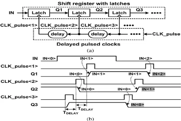
Fig. 3 Shift register with latches, delay circuits, and a pulsed clock signal. (a) Schematic. (b) Waveforms.
Method II: Another solution is to add delay in clock signal, ie. Multiple non overlap delayed pulsed clock is used to enables each latch. Fig.4 (a) shows the architecture and (b) is the output wave form. From this wave form it is understood that the timing problem is eliminated.
Fig. 4 Shift register with latches and delayed pulsed clock signals. (a) Schematic. (b) Waveforms.
But the method I and method II solves the timing problem but take more power and area because of the delay circuits. Here the number of delay circuit is large.
ISSN(Online): 2319-8753 ISSN (Print): 2347-6710
I
nternational
J
ournal of
I
nnovative
R
esearch in
S
cience,
E
ngineering and
T
echnology
(An ISO 3297: 2007 Certified Organization)
Website: www.ijirset.com
Vol. 6, Issue 4, April 2017
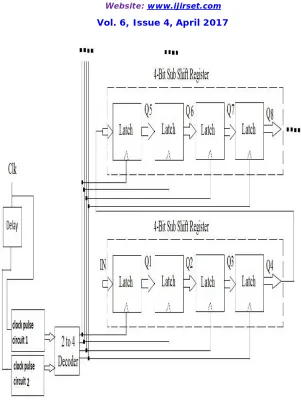
Fig.5 shift register. (a) Schematic. (b) Waveforms[4]
In this method the m bit shift register is divided in to 4 bit sub-shift register and each sub shift register consist of 5 latches from this one latches are used for temporary storage. And the clock pulse generator is used to enable the pulsed clock signal. Pulsed clock generator has 5 clock pulse circuit and each clock pulse circuit consist of a delay circuit, two inverter, a AND gate and a buffer. This method is better than the previous method. But it also use more area for temporary storage latches and pulsed clock generator circuit.
III PROPOSED SHIFT REGISTER
ISSN(Online): 2319-8753 ISSN (Print): 2347-6710
I
nternational
J
ournal of
I
nnovative
R
esearch in
S
cience,
E
ngineering and
T
echnology
(An ISO 3297: 2007 Certified Organization)
Website: www.ijirset.com
Vol. 6, Issue 4, April 2017
Fig. 6 proposed shift register using decoder enabled pulsed latch
ISSN(Online): 2319-8753 ISSN (Print): 2347-6710
I
nternational
J
ournal of
I
nnovative
R
esearch in
S
cience,
E
ngineering and
T
echnology
(An ISO 3297: 2007 Certified Organization)
Website: www.ijirset.com
Vol. 6, Issue 4, April 2017
Fig.7 Delayed clock pulse generator using decoder
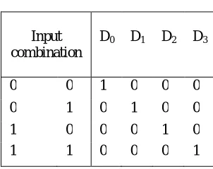
A binary decoder is a combinational logic circuit that converts a binary integer value to an associated pattern of output bits. It will convert binary information from n input signals to as many as 2n unique output signals. In this application a decoder has 2 input and 4 outputs that combination is shown in table 1.
Table 1: Truth table of decoder
Input combination
D0 D1 D2 D3
0 0 1 0 0 0 0 1 0 1 0 0 1 0 0 0 1 0 1 1 0 0 0 1
A0 and A1 are inputs And D0-D3 are outputs, both inputs are 0 then get D0 as high, A0 is 0 and A1 is 1 then D1 is high,
A0 is 1 and A1 is 0 then D2 is high and both inputs are 1 then get D3 is high. These output are act as delayed clock pulse
for the proposed shift register. The input of decoder, A0 and A1 signals are generated by the clock pulse circuits from
the main clock.
IV. RESULT AND DISCUSSION
ISSN(Online): 2319-8753 ISSN (Print): 2347-6710
I
nternational
J
ournal of
I
nnovative
R
esearch in
S
cience,
E
ngineering and
T
echnology
(An ISO 3297: 2007 Certified Organization)
Website: www.ijirset.com
Vol. 6, Issue 4, April 2017
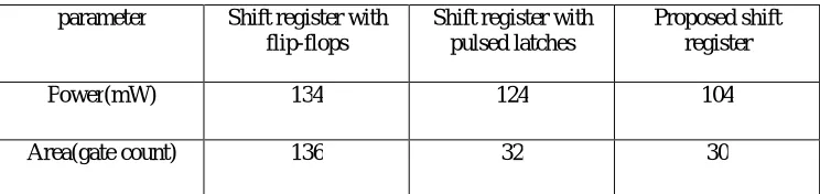
Table 2 Power and Area comparison.
parameter Shift register with flip-flops
Shift register with pulsed latches
Proposed shift register
Power(mW) 134 124 104
Area(gate count) 136 32 30
From the comparison table 2, the proposed shift register based on decoder enabled pulsed latch can save more power and area than conventional shift register using flip-flops. The shift register based on latches are more suitable for low power VLSI applications and it also reduces the chip size.
V. CONCLUSION
From the analysis the shift register with latches can reduce the area and power. The proposed 16- bit shift register consumes more the power and area than the conventional shift register using flip-flops and other methods with latches. The proposed shift register is constructed using pulsed latches, each latches are enabled using decoder. Here the 16 bit shift register is divided into 4 bit sub shift registers and the main clock is changed to delayed non-overlap multiple pulses that can solve the timing problem in the latches. The delayed clock pulses are generated using two clock pulse circuit and a 2:4 decoder it can reduce area and power more efficiently. This type of arrangement is less complex and simple than other conventional methods. It can save more power and area compared conventional shift registers used by flip-flops and other pulsed latches methods.
REFERENCES
[1] M. Hatamian et al., “Design considerations for gigabit ethernet 1000 base-T twisted pair transceivers,” Proc. IEEE Custom Integr. Circuits Conf., pp. 335–342, 1998.
[2] H. Yamasaki and T. Shibata, “A real-time image-feature-extraction and vector-generation vlsi employing arrayed-shift-register architecture,”
IEEE J. Solid-State Circuits, vol. 42, no. 9, pp. 2046–2053, Sep. 2007.
[3] P. Reyes, P. Reviriego, J. A. Maestro, and O. Ruano, “New protection techniques against SEUs for moving average filters in a radiation environment,” IEEE Trans. Nucl. Sci., vol. 54, no. 4, pp. 957–964, Aug. 2007.
[4] Byung-Do Yang “low power and area efficient shift register using pulsed latches,” IEEE Transactions on circuits and systems-1 regular papers,vol.62,no.6, pp.1564-1570,June 2015.
[5] H.-S. Kim, J.-H. Yang, S.-H. Park, S.-T. Ryu, and G.-H. Cho, “A 10-bit column-driver IC with parasitic-insensitive iterative charge-sharing based capacitor-string interpolation for mobile active-matrix LCDs,” IEEE J. Solid-State Circuits, vol. 49, no. 3, pp. 766–782, Mar. 2014. [6] S.-H. W. Chiang and S. Kleinfelder, “Scaling and design of a 16-megapixel CMOS image sensor for electron microscopy,” in Proc. IEEE
Nucl. Sci. Symp. Conf. Record (NSS/MIC), 2009, pp. 1249–1256.
[7] S. Heo, R. Krashinsky, and K. Asanovic, “Activity-sensitive flip-flop and latch selection for reduced energy,” IEEE Trans. Very Large Scale Integr. (VLSI) Syst., vol. 15, no. 9, pp. 1060–1064, Sep. 2007.
![Fig. 1 (a) Master-slave flip-flop. (b) Pulsed latch.[7]](https://thumb-us.123doks.com/thumbv2/123dok_us/1610822.1199591/2.595.156.440.496.648/fig-master-slave-flip-flop-b-pulsed-latch.webp)