Scholarship@Western
Scholarship@Western
Electronic Thesis and Dissertation Repository
3-6-2013 12:00 AM
Carbon Nitride and Conjugated Polymer Composite Materials
Carbon Nitride and Conjugated Polymer Composite Materials
Josh Byers
The University of Western Ontario
Supervisor Oleg Semenikhin
The University of Western Ontario Graduate Program in Chemistry
A thesis submitted in partial fulfillment of the requirements for the degree in Doctor of Philosophy
© Josh Byers 2013
Follow this and additional works at: https://ir.lib.uwo.ca/etd
Part of the Condensed Matter Physics Commons, Materials Chemistry Commons, Physical Chemistry Commons, Polymer and Organic Materials Commons, Polymer Chemistry Commons, and the
Semiconductor and Optical Materials Commons
Recommended Citation Recommended Citation
Byers, Josh, "Carbon Nitride and Conjugated Polymer Composite Materials" (2013). Electronic Thesis and Dissertation Repository. 1135.
https://ir.lib.uwo.ca/etd/1135
This Dissertation/Thesis is brought to you for free and open access by Scholarship@Western. It has been accepted for inclusion in Electronic Thesis and Dissertation Repository by an authorized administrator of
by
Joshua Byers
Graduate Program in Chemistry
A thesis submitted in partial fulfillment of the requirements for the degree of
Doctor of Philosophy
The School of Graduate and Postdoctoral Studies The University of Western Ontario
London, Ontario, Canada
ii
Abstract
The semiconductor and photovoltaic properties of carbon nitride (CNx) thin films prepared
using a reactive magnetron sputtering technique were investigated both individually and as
composites with the organic conjugated polymers polybithiophene (PBT) and
poly(3-hextlthiophene) (P3HT). At low nitrogen content, the film structure was dominated by
graphitic sp2 percolation networks, whereas at higher nitrogen contents CNx films started to
demonstrate semiconductor properties, as evidenced by the occurrence of photoconductivity
and the development of a space charge region. When CNx was deposited onto a PBT
substrate, it was found to function as an acceptor material improving the photocurrent
generation both in solution and in solid state photovoltaic devices, with the external quantum
efficiencies reaching 1% at high nitrogen contents. The occurrence of the donor–acceptor
charge transfer was further evidenced by suppression of the n-doping of the PBT polymer by
CNx. Nanoscale atomic force microscopy (AFM) and current-sensing AFM data suggested
that CNx may form a bulk heterojunction with PBT. Thermal annealing of nitrogen rich CNx
films led to n-type semiconductor materials consisting of a graphitic carbon nitride network
as determined using X-ray photoelectron spectroscopy, and these materials exhibited
photovoltaic properties.
Intensity modulated photocurrent (IMPS) and photovoltage (IMVS) spectroscopies were
used to study the mechanism of photoprocesses in P3HT:PCBM ([6,6]-phenyl C61 butyric
acid methyl ester ) bulk heterojunction organic solar cells at various light intensities. The use
of the frequency domain techniques allowed us to separate the bulk and interfacial processes
and gain valuable insight into the mechanism of losses in these devices. The results provide
direct evidence that interfacial nongeminate recombination is one of the dominant loss and
aging mechanisms in bulk heterojunction organic solar cells. The trapping of photoexcited
holes in the P3HT phase was found to contribute to the increased recombination rate. It was
determined that interfacial recombination occurs at the P3HT/PCBM interface and that
higher PCBM contents help to improve charge carrier extraction. The results suggest that
promising ways of improving the efficiency of bulk heterojunction solar cells may be
reducing the charge trapping both at and near the P3HT:PCBM interface, as well as
iii
iv
Co-Authorship Statement
All of the experimental work was carried out by Joshua Byers under the direction and supervision of Dr. Oleg Semenikhin except where noted below. All of the chapters in this thesis were originally written, edited, and revised by Joshua Byers under the supervision of Dr. Oleg Semenikhin who was actively involved in all steps through the entire process.
Chapter 3. A. Pailleret assisted with editing and revising the manuscript. F. Billon deposited CNx substrates for XPS collection and analysis by C. Debiemme-Chouvy for the data shown in the supporting information for Chapter 3 in the appendix. S. Borensztajn carried out SEM of CNx films for thickness determination shown in the supporting information for Chapter 3 in the appendix.
Chapter 4. M. Biesinger carried out XPS experiments and peak fitting.
Chapter 5. S. Ballantyne prepared bulk heterojunction photovoltaic devices and characterized them using an AM 1.5 Solar Simulator.
v
First and foremost I must sincerely thank my supervisor Dr. Oleg Semenikhin for providing
an excellent research environment along with tremendous opportunity to explore several
related areas of research to the work presented. I have learned a tremendous amount under
your mentorship and guidance over the years and greatly enjoyed your enthusiasm for
science. I would also like to thank all of the members of the Semenikhin group (Trissa,
Kevin, Radu, Adam, John, Mike) over the years for making the lab/office more than just an
enjoyable place to be each day.
This work represents the effort of several collaborative projects and I would like to thank all
of those involved. Dr. Alain Pailleret is gratefully acknowledged for his host supervision
during several extended visits to his laboratory at the University of Pierre and Marie Curie
where I was able to benefit from his experience and knowledge in the fabrication of carbon
nitride thin films. As well, I must thank Alex Mann and Konstantin Rodionov who I had the
pleasure of working with and for providing a glimpse into the exciting world of a start-up
company.
Finally, I must thank my family and in particular my wife Danielle who has been an
unwavering source of support over this entire journey. I dedicate this work to you.
Funding provided from the Department of Chemistry, The University of Western Ontario, the
Ontario Graduate Scholarship program and the France Government are gratefully
vi
Table of Contents
Abstract ... ii
Acknowledgments ...v
List of Tables... ix
List of Figures ...x
List of Appendices ... xvii
List of Abbreviations ... xviii
Chapter 1 ...1
1 Introduction ...1
1.1 Motivation for this work ...2
1.2 Scope of thesis ...4
1.3 References ...6
Chapter 2 ...7
2 Background...7
2.1 Organic Photovoltaics ...8
2.2 Bulk Heterojunction Polymer Solar Cells ... 11
2.3 Loss Mechanisms ... 15
2.4 Methods of Improvement ... 17
2.5 Carbon Thin Film Materials ... 19
2.6 Carbon Nitride ... 20
2.7 Methods to Study Photovoltaic Devices ... 24
2.7.1 Steady-State Current-Voltage Measurements ... 24
2.8 Frequency Domain Techniques ... 27
2.8.1 Electrochemical Impedance Spectroscopy ... 27
vii
Chapter 3 ... 43
3 Photocurrent Generation in Carbon Nitride and Carbon Nitride/Conjugated Polymer Composites ... 43
3.1. Introduction... 44
3.2. Experimental ... 46
3.3 Results and Discussion ... 49
3.4 Conclusions... 65
3.5 References ... 66
Chapter 4 ... 71
4 Nitrogen Rich Carbon Nitride Photovoltaic Materials ... 71
4.1 Introduction ... 72
4.2 Experimental ... 75
4.3 Results and Discussion ... 77
4.4 Conclusions ... 104
4.5 References ... 105
Chapter 5 ... 109
5 The Mechanism of Recombination Losses in Bulk Heterojunction P3HT:PCBM Solar Cells Studied Using Intensity Modulated Photocurrent Spectroscopy ... 109
5.1 Introduction ... 110
5.2 Experimental ... 113
5.3 Results and Discussion ... 117
5.4 Conclusions ... 136
5.5 References ... 138
viii
6 Influence of Preparation Conditions of Bulk Heterojunction Solar Cells Studied using
Intensity Modulated Photocurrent Spectroscopy ... 141
6.1 Introduction ... 142
6.2 Experimental ... 144
6.3 Results ... 145
6.4 Discussion... 159
6.5 References ... 170
Chapter 7 ... 172
7 Conclusions ... 172
7.1 Conclusions ... 173
7.2 Future Work ... 175
ix
Table 4-2. Binding energies and peak areas for peaks used to fit N 1s spectra. ...100
Table 4-3. Binding energies and peak areas for peaks used to fit C 1s spectra. ...100
Table 6-1. Device efficiencies for bulk heterojunction devices measured shortly after
fabrication………..…147
Table 6-2. Device efficiencies for bulk heterojunction devices measured aging……….….149
Table 6-3. Values for the low frequency ReJ0, high frequency gac, and (1 – γ) determined
from the IMPS plots………...………156
Table 6-4. Values for the rate constant for charge transfer ktr from the surface states to the Al
x
List of Figures
Figure 2-1. Bi-layer architecture. (a) Two materials with different ionization
potentials/electron affinities. (b) Light absorption and exciton formation (c) Charge transfer
and exciton dissociation. ... 10
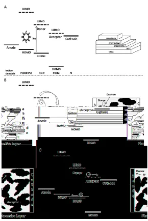
Figure 2-2. (A) Left: Absorption of light by donor material. Right: Solid state photovoltaic
device. (B) Right: Exciton splitting at donor acceptor interface. Left: Exciton diffusion in
donor material to acceptor interface. Dark area is acceptor material. Light area is donor
material. (C) Right: Electron is transported to cathode through the LUMO and hole is
transported to anode through the HOMO. Left: Electron transport through acceptor material
to cathode and hole transport through donor material to anode. ... 13
Figure. 2-3. Chemical structures of (A) poly(3-hexylthiophene), (B)
poly(3,4-ethylenedioxythiophene) and (C) phenyl-C61-butyric acid methyl ester. ... 14
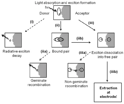
Figure 2-4. Bulk heterojunction active layer showing donor (white) and acceptor (grey)
interface. Illustration of (i) exciton decay, (ii) charge transfer state formation and (iii) exciton
dissociation in an organic bulk heterojunction device. Adapted from Ref. 21. ... 16
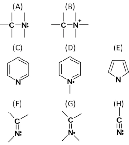
Figure 2-5. Different possible bonding arrangements in nitrogen doped t:aC and carbon
nitride. Only bonding arrangements (B), (D), and (G) in the centre column represent the
possible doping configurations... 22
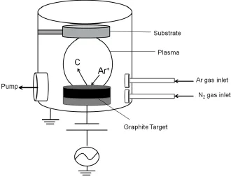
Figure 2-6. Illustration of the magnetron sputtering process. ... 24
Figure 2-7. Illustration of a JV curve obtained under illumination showing the open circuit
voltage Voc, the short-circuit current Isc, the point along the curve where the maximum power
is generated Pmax. The dotted square represents the area covered within the fill factor FF. .. 25
Figure 2-8. Example of a (A) Nyquist plot and corresponding Bode plots of (B) the
impedance magnitude |Z| and phase angle φ. The values for the elements used to generate
xi
organic solar cell and can be used to fit the data shown in Figure 2-8. ... 30
Figure 2-10. Photocurrent transients on the left and their complex plot representation on the
right. (A) Left: Light is switched on and immediately reaches steady state. Right:
Corresponding IMPS plot is located on real axis with no phase shift. (B) Left: Photocurrent
spikes when light is switched on and then decays. Right: IMPS plot is located in the first
quadrant in this case (C) Left: Photocurrent lags light intensity and slowly rises with time.
Right: The IMPS plot is located in the fourth quadrant in this case... 35
Figure 2-11. A typical IMPS spectrum shown in Nyquist plot representation. The IMPS
curve begins at the origin at a high frequency and moves across the fourth quadrant until it
crosses over at the real axis into the first quadrant and eventually reaches the steady-state
value ReJ0. ... 36
Figure 2-12. Schematic illustrating (i) charge carrier collection at the electrodes, and (ii)
charge carrier trapping at an interfacial state leading to (iia) extraction or (iib) interfacial
recombination. Adapted from Ref. 59. ... 37
Figure 3-1. Conductivity of CNx films as a function of N2 content in the gas mixture for films
prepared with a deposition power of 25 W (plot 1), 50 W (plot 2), 100 W (plot 3) during
deposition. The deposition time for all films was 20 minutes. The lines are guides for the eye.
... 50
Figure 3-2. Dark conductivity (plot 1) and photoconductivity (plot 2) for ITO/CNx/Au. CNx
was prepared at 100 W and 50 % N2. ... 52
Figure 3-3. (A) Mott-Schottky plot for CNx on an ITO substrate in aqueous 0.1 M KCl. CNx
was prepared at 50 W and 25 % N2. (B) Donor density determined from slopes of
Mott-Schottky plots for CNx films as a function of nitrogen content for deposition powers of 25 W
(■), 50 W (●) and 100 W (▲). ... 55
Figure 3-4. Energy level diagram of a CNx/PBT interface illustrating the proposed
xii
Figure 3-5. Net photocurrent generation of PBT/CNx composites on ITO substrates in
aqueous 0.1 M KCl. CNx films were prepared at 25 W and nitrogen contents of 5 % (plot 1),
25 % (plot 2), and 50 % (plot 3). Photocurrent generation of a pristine PBT film is included
for comparison (plot 4). ... 59
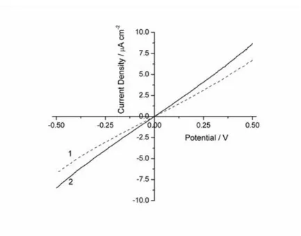
Figure 3-6. Current-Voltage plot of a solid state ITO/PEDOT/PBT/CNx/Al (plot 1) and a
ITO/PEDOT/PBT/Al (plot 2) photovoltaic device. CNx film was prepared at 25 W and 10 %
N2. ... 60
Figure 3-7. Quantum efficiency of PBT/CNx composites on ITO substrates in aqueous 0.1 M
KCl. CNx films were prepared at 25 W and nitrogen contents of 5 % (plot 1), 25 % (plot 2),
and 50 % (plot 3). A pristine PBT film is included for comparison (plot 4). Scan rate: 100
mV s-1. ... 61
Figure 3-8. 500 nm by 500 nm topography (left) and CS-AFM current (right) images of a
CNx film on PBT. A bias of + 500 mV was applied to the tip. Height scale bar: 200 nm.
CS-AFM current scale bar: 50 pA. ... 63
Figure 3-9. Cyclic voltammograms of (1) ITO/PBT and (2) ITO/PBT/CNx in acetonitrile and
0.1 M TBAPF6... 64
Figure 4-1. Dark J-V plots of CNx films prepared at (A) 25 W, (B) 50 W, (C) 100 W and (D)
150 W for nitrogen plasma compositions indicated. ... 79
Figure 4-2. Dark J-V plots of CNx films prepared using a deposition power of 25 W and
nitrogen contents of (A) 1 % N2, (B) 50 % N2, (C) 100 % N2. ... 81
Figure 4-3. (A) Nyquist plot and (B) Bode plot of CNx films prepared at 25 W and nitrogen
content of 1 % N2, 5 % N2 and 100 % N2 (1 Pa total pressure). (C) Equivalent circuit
element used to fit the data. Applied potential was 0 V in dark. ... 82
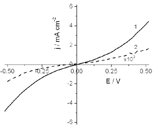
Figure 4-4. Illuminated (1) and dark (2) J-V plots of a CNx film prepared using a deposition
xiii
Note the current density of the aged film has been multiplied by a factor of 10 . ... 85
Figure 4-6. Nyquist plot of an aged CNx film prepared using a deposition power of 25 W in a
100 % nitrogen discharge plasma. ... 86
Figure 4-7. Dark (1) and illuminated (2) J-V plots of a CNx film prepared using a deposition
power of 25 W in a 100 % nitrogen containing plasma at 1 Pa after aging... 87
Figure 4-8. (A) Photocurrent and (B) photovoltage transients for photoconductive (plot 1 -
fresh) and photovoltaic (plot 2 - aged) CNx films prepared in 100 % N2 plasma at 1 Pa. ... 88
Figure 4-9. Dark current-voltage plots of CNx prepared at 1 Pa (plot 1), 3 Pa (plot 2) and 5
Pa (plot 3) pure nitrogen plasma discharge pressures. Current density values for films
prepared at 3 Pa and 5 Pa have been multiplied by a factor of 25 and 500 respectively to
more clearly display on the same plot. ... 90
Figure 4-10 Values for the (A) parallel capacitance and (B) parallel resistance as a function
of annealing temperature determined using a Randles equivalent circuit for CNx films
prepared at 1 Pa, 3 Pa, and 5 Pa pure nitrogen plasma discharge pressures. All films were
annealed for 60 minutes. (C) Figure 4-10A re-plotted as a function of total plasma pressure.
... 92
Figure 4-11. Typical J-V plot under illumination for CNx films prepared at 3 Pa (plot 1) and
5 Pa (plot 2) pure nitrogen plasma discharge pressures. The films were annealed for 60
minutes at 150oC. ... 94
Figure 4-12. Photocurrent transient for a CNx film at an applied bias of – 70 mV. The film
was prepared in a 5 Pa pure nitrogen discharge plasma and annealed for 60 minutes at 150oC.
... 96
Figure 4-13. (A) C 1s XPS spectrum for an as deposited CNx film prepared in a 5 Pa
discharge plasma. (B) N 1s XPS spectrum for an as deposited CNx film prepared in a 5 Pa
xiv
Figure 4-14. (A) C 1s XPS spectrum for an annealed CNx film prepared in a 5 Pa discharge
plasma. Films were annealed for 60 minutes at 150oC. (B) N XPS 1s spectrum for an
annealed CNx film prepared in a 5 Pa discharge plasma. Films were annealed for 60 minutes
at 150oC. ...102
Figure 4-15. Photocurrent transients for a CNx single layer device (plot 1), P3HT single layer
device (plot 2) and a CNx-P3HT heterojunction device (plot 3) measured at short-circuit
conditions. All films were annealed at 150oC for 60 minutes. ...104
Figure 5-1. Experimental I-V curves for two P3HT:PCBM cells after fabrication (plot 1, cell
B; plot 2, cell A) prepared on the same photovoltaic slide. ...118
Figure 5-2. (A) Experimental IMPS spectra obtained at short-circuit conditions for two
P3HT:PCBM photovoltaic cells (plot 1, cell A; plot 2, cell B) prepared on the same
photovoltaic slide. (D) Comparison of experimental IMPS spectra for cell A (1) after
fabrication and (2) after ageing for 2 months. The arrows indicate the direction of increasing
frequency. IMPS spectra are presented as Bode plots of (B,E) the imaginary and (C,F) the
real components of the photocurrent response vs. the modulation frequency. The dc light
intensity for all spectra was 8.2×10¹⁵ s-1cm-2. ...122
Figure 5-3. The intensity dependence of IMPS spectra measured at short-circuit conditions
for photovoltaic cell A. The dc light intensities were (1) 8.2×10¹⁵ 1cm-2; (2) 2.2×10¹⁶
s-1cm-2; (3) 3.5×10¹⁶ s-s-1cm-2; (4) 5.0×10¹⁶ s-1cm-2 and (5) 6.4×10¹⁶ s-1cm-2. The IMPS
spectra are presented as (A) a Nyquist complex plane plot as well as Bode plots of (B) the
imaginary and (C) the real components of the photocurrent response vs. the modulation
frequency. The arrow indicates the direction of increasing frequency. ...126
Figure 5-4. The intensity dependence of IMVS spectra measured at open-circuit conditions
for photovoltaic cell A. The dc light intensities were (1) 8.2×10¹⁵ s-1cm-2; (2) 2.2×10¹⁶ s-1cm
-2
; (3) 3.5×10¹⁶ s-1cm-2; (4) 5.0×10¹⁶ s-1cm-2 and (5) 6.4×10¹⁶ s-1cm-2. The IMVS spectra are
presented as (A) a Nyquist complex plane plot as well as Bode plots of (B) the imaginary and
(C) the real components of the photovoltage response vs. the modulation frequency. (D)
xv
Figure 5-5. (A) Experimental IMPS spectra obtained at cell biases of 0.0 V (plot 1), +0.25 V
(plot 2), +0.5 V (plot 3) as well as Bode plots of (B) the imaginary and (C) the real
components of the photocurrent response obtained at these bias values vs. the modulation
frequency. ...130
Figure 5-6. Mott-Schottky plots for photovoltaic cell A measured in the dark (plot 1) and as a
function of the dc light intensity (plots 2-6). The light intensity values were (2) 8.21015 s
-1
cm-2; (3) 2.21016 s-1cm-2; (4) 3.51016 s-1cm-2; (5) 5.01016 s-1cm-2 and (6) 6.41016 s-1cm-2.
The inset shows an enlarged Mott-Schottky plot at a dc light intensity of 5.01016 s-1cm-2. 132
Figure 5-7. Dependencies on the dc light intensity of (A) interfacial recombination rate
constant derived from the IMPS plots and (B) trap density obtained from the Mott-Schottky
plots for photovoltaic cell A. For each graph, plot 1 corresponds to the photovoltaic cell after
ageing for 2 months and plot 2 corresponds to a photovoltaic cell after fabrication. ...134
Figure 6-1. J-V plots of encapsulated bulk heterojunction devices containing a P3HT:PCBM
mass ratio of (A) 1:0.5, (B) 1:0.6, (C) 1:0.7, and (D) 1:0.8. ...146
Figure 6-2. J-V plots of non-encapsulated bulk heterojunction devices containing a
P3HT:PCBM mass ratio of (A) 1:0.5, (B) 1:0.6, (C) 1:0.7, and (D) 1:0.8. ...147
Figure 6-3. J-V plots of aged non-encapsulated bulk heterojunction devices containing a
P3HT:PCBM mass ratio of (A) 1:0.5, (B) 1:0.6, (C) 1:0.7, and (D) 1:0.8. ...149
Figure 6-4. Experimental IMPS spectra obtained at short-circuit conditions for a
P3HT:PCBM ratio of 1:0.7 in (A) Nyquist and (B,C) Bode plot representation. The dc light
intensity used was (1) 3.07x10¹⁶, (2) 1.62x10¹⁷, and (3) 2.95x10¹⁷ s-1 cm-2...151
Figure 6-5. The value of the rate constant for recombination ω* for P3HT:PCBM mass ratios
of 1:05, 1:0.6, 1:0.7 and 1:0.8 as a function of the dc light intensity. The line is not a fit and is
xvi
Figure 6-6. Experimental IMPS spectra obtained at short-circuit conditions for P3HT:PCBM
ratios of (1) 1:0.5, (2) 1:0.6, (3) 1:0.7, and (4) 1:0.8 in (A) Nyquist and (B,C) Bode plot
representation. The dc light intensity for all spectra was 1.62x10⁻¹⁷ s-1 cm-2. ...154
Figure 6-7. Normalized IMPS spectra (from Figure 6-6 (A)) obtained at short-circuit
conditions for P3HT:PCBM ratios of (1) 1:0.5, (2) 1:0.6, (3) 1:0.7, and (4) 1:0.8 in Nyquist
plot representation. The dc light intensity for all spectra was 1.62x10⁻¹⁷ s-1 cm-2. The high
frequency intercept gac, low frequency intercept 1-γ and the maximum of the imaginary
photocurrent ω* are indicated . ...155
Figure 6-8. Experimental IMPS spectra of aged films obtained at short-circuit conditions for
P3HT:PCBM ratios of (1) 1:0.5, (2) 1:0.6, (3) 1:0.7, and (4) 1:0.8 in (A) Nyquist and (B,C)
Bode plot representation. The dc light intensity for all spectra was 1.62x10⁻¹⁷ s-1 cm-2. ...157
Figure 6-9. Normalized IMPS spectra of aged films obtained at short-circuit conditions for
P3HT:PCBM ratios of (1) 1:0.5, (2) 1:0.6, (3) 1:0.7, and (4) 1:0.8 in (A) Nyquist and (B,C)
Bode plot representation. The dc light intensity for all spectra was 1.62x10⁻¹⁷ s-1 cm-2. ...159
Figure 6-10. (A) Short-circuit current density and (B) open-circuit voltage as a function of
PCBM content for (1) fresh cells and (2) aged cells. A light intensity of 1.62x10¹⁷ s-1 cm-2
was used. ...160
Figure 6-11. Schematic showing the possible interfaces where interfacial recombination may
occur in a bulk heterojunction P3HT:PCBM device. ...162
Figure 6-12. (A) Values for the (1) high frequency intercept gac and the (2) low frequency
intercept ReJ0 for aged cells as a function of PCBM content in the film. (B) Fraction of
charge carriers collected as a function of PCBM content for (1) fresh cells and (2) aged cells.
xvii
Nitride and Carbon Nitride Conjugated/Polymer Composites ...177
Appendix B: Copyright Release from Publisher for Chapter 3 ...184
xviii
List of Abbreviations
Abbreviation Definition
A electrode surface area
AFM atomic force microscopy
AM air mass
BDD boron doped diamond
BE binding energy
BT 2,2-Bithiophene
Bu4NPF6 tetrabutylammonium hexafluorophosphate
CB conduction band
CELIV charge extraction by linearly increasing voltage
cm centimetre
CNx carbon nitride
C capacitance
Cp parallel capacitance
CS-AFM current-sensing atomic force microscopy
CSC space-charge capacitance
CV cyclic voltammetry
DC direct current
DLC Diamond like carbon
eo elementary charge
e- electron
Ef Fermi level
Efb flat-band potential
Eg band-gap
EIS electrochemical impedance spectroscopy
ε dielectric constant
εo permittivity of free space
eV electron volt
gac high frequency photocurrent
xix
h hole
HOMO highest occupied molecular orbital
Hz hertz
Imax photocurrent at maximum power
IMPS intensity modulated photocurrent spectroscopy
IMVS intensity modulated photovoltage spectroscopy
ISC short-circuit current density
ITO indium tin oxide
j imaginary part
J current density
κ Boltzmann constant
kHz kilohertz
LUMO lowest unoccupied molecular orbital
M molar
m metre
μA microampere
ml millilitre
mm millimetre
mV millivolt
mW milliwatt
ηe efficiency
N newton
NA acceptor density
ND donor density
nm nanometre
ω circular frequency
Ω ohm
OPV organic photovoltaic
P3HT poly(3-hexylthiophene)
xx
PBT polybithiophene
PCBM [6,6]-phenyl C61 butyric acid methyl ester
PEDOT:PSS poly(3,4-ethylenedioxythiophene):polystyrene sulfonate
Φ phase shift
Pin power in
PMax maximum power point
π pi bonding orbital
π* pi antibonding orbital
ps picosecond
σ sigma bonding orbital
σ* sigma antibonding orbital
ReJ0 low frequency photocurrent
RF radiofrequency
Rp parallel resistance
Rs serial resistance
s second
SCCM standard cubic centimeters per minute
SCE saturated calomel electrode
SEM scanning electron microscope
t:aC tetrahedral amorphous carbon
T absolute temperature
TOF time of flight
V volt
Vmax voltage at maximum power
VOC open-circuit voltage
VB valence band
W watt
XPS X-ray photoelectron spectroscopy
1.1
Motivation for this work
As the demand for energy continues to grow it is evident that new sources will be needed
in the future to continue to satisfy the world’s energy needs. Furthermore, it is becoming
increasingly clear that anthropogenic green house gases are having a detrimental impact
on our climate, which makes the development of sustainable energy sources an important
global goal. It has been suggested, that by 2050, the world energy demand could reach 60
terawatts, which is the equivalent of 900 million barrels of oil per day. The anticipated
need for this overwhelmingly large amount of energy has been referred to as “The
Terawatt Challenge”.1
This type of demand will undoubtedly only be met through a
combination of traditional energy sources such as oil, hydroelectric, coal, gas, and
fission, along with renewables such as wind, solar and geothermal energy playing an
increasingly prevalent role. Ultimately, economics will to a large extent determine the
most likely energy sources that are used in the future and therefore the development of
renewable energy sources using low cost and high-throughput methods represent a
promising path towards this goal.
Photovoltaic devices represent a vital part of a sustainable future and are based on the
separation of charge at the interface of two materials as a result of light absorption in one
or both materials. Commercially available solar cells, often referred to as generation one
and generation two devices, use solid state architectures made from inorganic materials.
The main drawbacks of these technologies include high processing costs, the use of toxic
materials in some cases and an inability to generate a large and significant source of
energy due to manufacturing limitations.2,3 However, third generation devices, which
take advantage of nanostructured films and organic materials are being intensely
investigated for potential low cost, high throughput solar energy generation for large
scale exploitation.4 The realization of efficient and practical photovoltaic systems for
energy conversion requires the continued development and understanding of new
materials that can be used on a large scale, while remaining economically viable.
Photovoltaic devices based on conjugated polymers continue to generate significant
interest due to their potential application as a low cost material combined with high
potential of organic solar cells. However, the lifetimes of these devices are still very low
and remain a significant barrier toward their large scale production. The understanding
and knowledge of the loss mechanisms in these devices is much more limited and
represents an important area of research where new methods and techniques are needed
to study these nanostructured devices.
The generation of free charge carriers in organic photovoltaic devices is quite different
from that of many other traditional solar cells such as silicon due to the increased exciton
binding energy in organic materials. Organic photovoltaic devices typically consist of a
conjugated polymer mixed with a fullerene derivative to maximize charge carrier
generation by solar radiation. The most efficient polymer solar cells combine these two
materials with a nanoscale phase separation on the order of 10’s of nm’s to form a
composite photoactive layer. The photoactive layer is sandwiched between two selective
contacts for electron and hole extraction resulting in the formation of a bulk
heterojunction organic solar cell. To improve charge carrier extraction, interfacial
materials between the anode and/or cathode are often employed. The introduction of
these layers increases the number of thin film materials and interfaces in these devices
that photogenerated charge carriers must be efficiently transported to and across. It is
very important to understand the dynamics of charge transport across these interfaces to
develop more effective interfacial materials that will continue to improve the efficiency
of organic solar cells. A powerful technique that had not been applied to the investigation
of bulk heterojunction polymer photovoltaic devices at the commencement of this thesis
was intensity modulated photocurrent spectroscopy (IMPS). Intensity modulated
photocurrent spectroscopy is a technique where the complex ratio of photocurrent flux to
incident light flux is measured over many decades of frequency using a frequency
response analyzer. Analysis of these spectra provides insight into the parameters that
control charge transport and recombination at the interfaces in bulk heterojunction
The vast majority of organic photovoltaic devices employ a fullerene derivative as an
acceptor material in combination with a donor conjugated polymer. However, in
polymeric photovoltaic devices, the majority of light absorption is due to the p-type
donor polymer and not fullerenes. One of the advantages of using conjugated organic
polymers is a high absorption coefficient that can be tuned to match the solar spectrum.
Due to the large volume of fullerenes in these devices, the amount of light absorbing
polymer is greatly reduced in the active layer, which ultimately limits the amount of light
that can be absorbed. The constraints of high loading ratios combined with the low solar
absorbance of fullerenes present an important area of improvement for future devices.
Therefore new materials that can act as effective electron acceptor materials similar to
fullerenes while also contributing a significant amount towards photocurrent generation
represents an extremely important goal in the realization of more efficient organic
photovoltaic devices. Another disadvantage of fullerenes is that they are small molecules
rather than continuous materials, and therefore any nanostructure formed with fullerenes
will be prone to morphological changes, phase segregation, etc. Carbon nitride (CNx) is a
potentially promising material for this type of application as it has been shown to exhibit
semiconductor properties that could be beneficial for use in a photovoltaic device.
However, very little work has been done in this area with no reports of composite organic
photovoltaic devices based on these materials having been studied prior to the
commencement of this thesis. It is shown in this work for the first time that n-type carbon
nitride materials can be developed that exhibit photovoltaic properties and function as an
electron acceptor material when combined with a conjugated polymer.
1.2
Scope of thesis
This thesis examines two very important issues in the development of photovoltaic solar
cells including the development of new photovoltaic materials and new methods for
studying charge transport and recombination in these devices.
Chapter 2 provides a brief overview of the development of organic solar cells and the key
milestones that have guided research in this field. As mentioned, there is a need for the
development of alternative acceptor and semiconductor materials for photovoltaic solar
provided. Many of the measurements carried out in this thesis use frequency resolved
techniques to study the dynamic processes occurring in organic photovoltaic materials
and devices, and an overview of their application to photovoltaic devices is included.
In Chapters 3 and 4 the semiconductor and photovoltaic properties of carbon nitride
(CNx) thin films prepared using a reactive magnetron sputtering technique were
investigated both individually and as composites with the organic conjugated polymers,
poly(2,2′-bithiophene) (PBT) and poly(3-hexylthiophene) (P3HT). When CNx was
combined with a conjugated polymer they were shown to function as an acceptor material
leading to an increase in photocurrent generation in the composite materials. The
influence of the deposition conditions (target power, nitrogen partial pressure, and total
pressure) was studied to understand their role on the resulting optical and electronic
properties of the thin film materials. The elimination of graphitic percolation networks
accompanied by improved structural ordering led to nitrogen rich carbon nitride materials
that exhibited photoconductive and photovoltaic properties. Structural ordering was
promoted through film relaxation using thermal annealing that led to fabrication of single
layer photovoltaic carbon nitride thin film materials. This represents the first
demonstration of a photovoltaic effect in carbon nitride thin film materials prepared using
reactive magnetron sputtering. A prototype p-n heterojunction device made up of a p-type
P3HT layer and n-type CNx layer was shown to exhibit enhanced photovoltaic properties
relative to either of the single layer devices demonstrating the potential of CNx as a new
type of photovoltaic solar cell material.
In Chapters 5 and 6 intensity modulated photocurrent (IMPS) and photovoltage (IMVS)
spectroscopies were used to study the mechanism of photoprocesses in P3HT:PCBM
(Phenyl-C61-Butyric-Acid-Methyl Ester) bulk heterojunction organic solar cells
containing varying amounts of P3HT and PCBM in the active layer. The use of the
frequency domain techniques allowed us to separate the bulk and interfacial processes
and gain valuable insight into the mechanism of losses in these devices. The results
dominant loss and aging mechanisms in bulk heterojunction organic solar cells. It is also
shown that high loading ratios of PCBM are beneficial for the enhanced stability of
organic solar cells with device aging. This is attributed to improved carrier extraction at
the interface between PCBM and the metal cathode, which limits the amount of charge
carriers that are lost to interfacial recombination. These results demonstrate the
importance of the PCBM content on device stability, an important aspect, which is often
overlooked in the search for alternative acceptor materials.
Chapter 7 summarizes the main conclusions reached in this thesis and considers their
significance in the context of the development of high stability and efficient organic solar
cells and discusses future directions of research that build upon the results presented.
1.3
References
(1) Smalley, R. E. MRS Bulletin.2005, 30, 412.
(2) Zweibel, K. Science2010, 328, 699.
(3) Peter, L. M. Philosophical Transactions of the Royal Society, A 2011, 369, 1840.
(4) Kamat, P. V. Journal of Physical Chemistry C2007, 111, 2834.
(5) Small, C. E.; Chen, S.; Subbiah, J.; Amb, C. M.; Tsang, S. W.; Lai, T. H.; Reynolds,
J. R.; So, F. Nature Photonics2012, 6, 115.
(6) Sondergaard, R.; Hosel, M.; Angmo, D.; Larsen-Olsen, T. T.; Krebs, F. C. Materials
.
2.1
Organic Photovoltaics
Organic photovoltaic devices are a promising platform for the conversion of solar energy
into electricity as these materials can be synthetically tailored permitting molecular
control of the electronic and optical properties. Many of the early organic solar cells were
fabricated using small organic molecules such as phthalocyanines and merocyanines.1
The simplest device architectures consisted of a single molecular organic active layer
sandwiched between two electrodes with different work functions, which were typically a
transparent semi-metallic material such as indium tin oxide (ITO) combined with a
second metal electrode. The difference in work function of the two electrodes generated
an electric field across the thin organic layer and helped to direct and transport the
photogenerated charge carriers through the active layer. While early devices
demonstrated the potential of organic materials in solar cells, their efficiencies were quite
low. These low efficiencies were attributed to the formation of excitons, instead of
separated electrons and holes as in conventional solar cell devices.2 An exciton is an
uncharged coulombically bound electron-hole pair and it is necessary to dissociate the
exciton into free charge carriers to generate a photocurrent. Exciton dissociation can
occur at the interface between two different materials. In the case of a single layer
organic solar cell, this interface is created between the organic material and the
electrode.3 Due to the short exciton lifetime and diffusion length, photocurrent generation
is confined to the organic/electrode interface representing a small fraction of the film,
which reduces the amount of material that can generate an electric current.
The formation of excitons in organic solar cells emphasizes the importance of different
dynamic processes compared to conventional solar cells such as silicon. The important
parameters affecting organic photovoltaic device efficiency include:
(1) Exciton generation
(2) Exciton diffusion length
(5) Charge extraction at the electrodes
The electrically neutral exciton has a limited diffusion length of approximately 5 – 10 nm
in conjugated polymers.4 Recombination of an exciton can occur if it is not separated into
a free electron and a hole, limiting the maximum attainable photocurrent. Typical binding
energies of an exciton are approximately 0.3 eV requiring a similar difference in energy
at the interface for dissociation to occur.5 Upon exciton dissociation, the negative and
positive charges must be transported across the active layer, to the proper electrodes.
Charge transport of free charge carriers across the film and their extraction at contacts,
represents a serious loss mechanism in these devices, especially with aging, and a part of
this thesis includes the development and use of the technique intensity modulated
photocurrent and photovoltage spectroscopy (IMPS/IMVS) to bulk heterojunction
organic solar cells to address these issues in further detail.6
A significant milestone in the development of organic photovoltaic devices occurred
through the demonstration of a bi-layer arrangement that significantly enhanced
photocurrent generation.7 This innovative device architecture consisted of two different
organic materials in the active layer. Due to differences in ionization potentials and
electron affinities in these materials, the dissociation of excitons at the organic/organic
interface was much more efficient. This led to increased photocurrent generation, with
device efficiencies approaching approximately 1 %. The bi-layer device architecture is
illustrated below in Figure 2-1 to demonstrate how excitons are generated and dissociated
at the interface of two different organic materials. The majority of organic solar cells
today exploit the differences in the HOMO/LUMO levels of two different materials to
Figure 2-1. Bi-layer architecture. (a) Two materials with different ionization
potentials/electron affinities. (b) Light absorption and exciton formation (c) Charge
transfer and exciton dissociation.
Figure 2-1A shows that before illumination the highest occupied molecular orbital
(HOMO) and lowest unoccupied molecular orbital (LUMO) of each organic material are
offset. The material with a smaller ionization potential is known as the electron donor,
while the material with a larger electron affinity is referred to as the electron acceptor.
Illumination of the organic materials with visible light leads to formation of an exciton,
which diffuses to the interface of the two organic materials (Fig. 2-1B). Dissociation of
the exciton at the donor-acceptor interface generates a negatively charged electron on the
acceptor material and a positively charged hole on the donor material. These charged
species then travel across the active layer towards the cathode and anode respectively to
generate a photocurrent (Fig. 2-1C). The bi-layer architecture marked a significant
advancement in the efficiencies of organic photovoltaic devices, but it still did not
overcome the problem of the short diffusion length of excitons in organic materials.
Excitons created farther away from this interface still did not contribute to the
photocurrent and limited the region of the light harvesting active layer to the immediate
vicinity of the donor-acceptor interface. Therefore, the conversion of photons into
electrons could not occur across the entire film, placing a significant limit on the
maximum achievable photocurrent in these devices. This was, amongst other reasons, one
of the major motivating factors for the development and application of conjugated
Due to their extended conjugated structure, conjugated polymers exhibit a high
absorption coefficient that is on the order of 105 cm-1 and as a result, a film of only ca.
200 nm is needed to absorb all photons at the peak absorption.8 Similar to organic small
molecules, their electronic and optical properties can be controlled through chemical and
electrochemical modification leading to materials with electronic properties that exhibit
exceptionally high conductivities similar to metals, as well as semi-conducting and
insulating properties.9 The use of conjugated organic polymers opens the door towards
the development of materials that combine the processability of polymers with useful
electronic and optical properties. Moreover, these materials can be deposited onto a
substrate directly from solution, which allows for the development of high-throughput
deposition techniques such as ink-jet printing, spray coating, electrochemical deposition,
etc.10 All of these factors highlight the significant driving force behind the development
and use of conjugated polymer materials in organic solar cells.
Two concepts demonstrated 15 – 20 years ago still underline the design and architecture
of the majority of organic polymer photovoltaic devices today. The first was the
demonstration that fullerenes were found to be extremely effective materials for
promoting the photoinduced electron transfer from a conjugated polymer to a fullerene
molecule as observed by photoluminescence quenching that was almost 100%
efficienct.11 Later it was shown that a similar bi-layer device containing a donor
conjugated polymer combined with a fullerene acceptor thin film generated a
heterojunction device that exhibited promising semiconductor and photovoltaic
properties.12 While these devices were still limited by the short diffusion length of
excitons, this early result paved the road toward the formation of an interpenetrating bulk
heterojunction active layer, which opened the way towards high efficiency organic solar
cells. A major shift in the fabrication of polymer solar cells occurred following the
demonstrations that a donor and acceptor conjugated polymer, or a donor conjugated
polymer mixed with a soluble fullerene acceptor phenyl-C61-butyric acid methyl ester
(PCBM), can be cast from the same solution to form a nanoscale interpenetrating
networks formed a 3-dimensional bulk heterojunction photoactive layer and maximized
the interfacial area between the two different materials, which led to significantly
enhanced exciton dissociation and photocurrent generation. It is the bulk heterojunction
active layer that is used in the vast majority of polymer solar cell architectures today,
with fullerenes and their derivatives being ubiquitous in their use in the most highly
efficient devices.15
The left hand side of Figure 2-2A illustrates the absorption of light by a semiconducting
conjugated polymer in a bulk heterojunction solar cell leading to the formation of an
exciton. The right hand side of Figure 2-2A shows the multi-layer structure that is typical
of a bulk heterojunction organic solar cell. A transparent conductor indium tin oxide is
coated onto a glass slide and this is the side of the photovoltaic device where light enters.
The light is absorbed by the photoactive layer, eventually leading to charge carriers being
generated, with holes being extracted at the ITO electrode and electrons being collected
at the low work function metal electrode, which is often aluminum in organic solar cells.
As mentioned above, dissociation of an exciton is necessary to create a free electron and
hole to generate a photocurrent. In polymer bulk heterojunction solar cells the conjugated
polymer is responsible for light absorption and this is where the exciton is formed, as
shown in Figure 2-2B. To separate the exciton, an acceptor material with a LUMO that is
lower in energy is combined in the bulk heterojunction to increase charge carrier
generation. In the right hand side of the diagram, the donor material (grey shading) is
poly(3-hexylthiophene) (P3HT) and the acceptor material (black shading) is PCBM,
which are two commonly used materials. Their structures along with the hole transport
material poly(3,4-ethylenedioxythiophene):polystyrene sulfonate (PEDOT:PSS) are
shown below in Figure 2-3. The free charge carriers produced in these devices occur due
to the separation of excitons at the donor/acceptor interface. Upon dissociation, the
negative and positive charge carriers must be transported to the proper electrodes through
percolation pathways in the bulk heterojunction. The positively charged holes are
transported by the donor material while the negatively charged electrons are transported
by the acceptor material to their respective electrodes as shown in Figure 2-2C. Due to
the high surface area of the heterojunction between the donor and acceptor materials,
Figure 2-2. (A) Left: Absorption of light by donor material. Right: Solid state
photovoltaic device. (B) Right: Exciton splitting at donor acceptor interface. Left:
Exciton diffusion in donor material to acceptor interface. Dark area is acceptor
material. Light area is donor material. (C) Right: Electron is transported to cathode
through the LUMO and hole is transported to anode through the HOMO. Left:
Electron transport through acceptor material to cathode and hole transport through
Figure. 2-3. Chemical structures of (A) poly(3-hexylthiophene), (B)
poly(3,4-ethylenedioxythiophene) and (C) phenyl-C61-butyric acid methyl ester.
The ideal morphology of bulk heterojunction solar cells should contain phase segregated
domains that are about twice the exciton diffusion length (10 – 20 nm) in size, and these
domains should also form a percolation network across the bulk of the film (100 – 200
nm) to ensure the transport of charge carriers to the corresponding electrodes.8 The film
morphology is a critical aspect that governs the interactions between the donor and
acceptor phases in the active layer.16,17 The photocurrent generation in films prepared
using the same composition of donor and acceptor materials but deposited from different
solvents can be markedly different, and this has been directly attributed to differences in
film morphology.18 This example highlights the extreme importance of film morphology
and composition on the efficiency of organic solar cells. Photoactive layers that do not
possess an optimum morphology can result in significantly reduced efficiencies due to
decreased photocurrent generation, charge carrier transport and poor contact formation
with the electrodes. All of these factors can limit device efficiency. However, methods
that are available to investigate the influence of film morphology and composition on
carrier transport and other dynamic processes under normal working conditions of bulk
heterojunction organic solar cells are not readily available, which has limited their
The time scales of the various processes occurring in organic solar cells span from the
femtosecond timescale to as long as several hundred milliseconds.19,20 The initial
processes of exciton formation and dissociation in bulk heterojunction active layers occur
on a very fast time scale and have been extensively studied using transient absorption
optical techniques.21 Figure 2-4 (as adapted from Ref. 21) highlights the different
possible paths that can lead to charge carrier extraction and the possible loss mechanisms
that can occur in a device following light absorption in the conjugated polymer.
Initially, there are three possible outcomes that can be considered for an exciton
following light absorption:
(i) Exciton recombination
(ii) Exciton separation at the donor/acceptor interface into an electron and a hole that
remain spatially correlated
(iii) Separation of an exciton into a free electron and hole
In case (i), light absorption by the polymer leads to exciton formation and subsequent
radiative decay before it is able to reach the donor/acceptor interface. In case (ii), an
exciton can reach the donor acceptor interface and form a charge transfer state that
remains electrically neutral. It is possible for this spatially correlated exciton to
recombine without generating a photocurrent (iia). This type of recombination is referred
to as geminate recombination because the electron recombines with the hole that it was
initially separated from. Alternatively, after forming this so called charge transfer state,
the exciton can be separated, leading to the generation of free charge carriers, which may
be transported across the film and extracted at the electrodes (iiib). It is also possible that
once created, the free charge carriers will not reach the electrodes upon their separation.
Instead, as shown in case (iiia), a positive and negative charge carrier that were
independently generated can recombine without being collected. This is referred to as
nongeminate recombination.22 Nongeminate recombination can occur for a variety of
formation, as well as interfacial states due to defects present in the film and at the
electrodes. Nongeminate recombination becomes an increasingly important problem in
organic photovoltaic devices when considering their long term stability.
Figure 2-4. Bulk heterojunction active layer showing donor (white) and acceptor
(grey) interface. Illustration of (i) exciton decay, (ii) charge transfer state formation
and (iii) exciton dissociation in an organic bulk heterojunction device. Adapted from
Ref. 21.
The realization of practical organic photovoltaic devices is not only limited by their low
efficiencies but also their short service life.23 However, the degradation of organic solar
cells has not been as well investigated, especially the dynamic processes such as
recombination and charge carrier transport. Typically, steady-state current voltage plots
understand the chemical and physical processes that accompany a decrease in efficiency.
While these techniques provide valuable insight into modifications of the active layer
morphology and interfacial degradation, they do not provide details of the processes that
limit the efficiency. Due to the high surface area interpenetrating nanoscale morphology,
there are many possible interfaces throughout the bulk of the film as well as at the charge
collecting electrodes where losses may occur. The identification of the loss mechanisms
is extremely important as it can provide insight into new methods and device
architectures that could be used to improve device stability. As discussed in further detail
in this thesis, intensity modulated photocurrent spectroscopy (IMPS) is a powerful
technique for probing processes that occur on a longer time scale, which represent
significant loss mechanisms in organic photovoltaic devices, especially with respect to
device stability. Using IMPS it is possible to probe and separate the dynamic processes of
charge carrier transport and interfacial recombination, which are not readily determined
using steady-state techniques such as current-voltage measurements under illumination.
2.4
Methods of Improvement
Improvements for organic photovoltaic devices have included the design and synthesis of
low band-gap polymers for absorption of a larger part of the solar spectrum,24
development of tandem or multilayer cells,25 improved light absorption of the electron
acceptor,26 optical spacers,27 processing additives,28 and control of the nanoscale phase
separation.29 A combination of these effects in a single layer device that exploits an
inverted architecture has led to the best reported efficiency in a polymer photovoltaic
solar cell in excess of 9%,30 and greater than 10 % in a tandem cell configuration.31 These
efficiencies are extremely encouraging and illustrate the tremendous potential of organic
solar cell devices. However, increasingly it is becoming more important that these types
of efficiencies are sustainable over several years, highlighting the need to understand how
and why efficiency decreases with time.23
A dramatic improvement in efficiency was realized through the bulk heterojunction
acceptor. PCBM is the ubiquitous acceptor material in organic photovoltaics and its
overwhelming use is due to the excellent electron transport and exceptional electron
accepting abilities of fullerenes.32,33 However, PCBM is itself a molecule and not a
polymer. As a result, high loading ratios of PCBM are required to create conducting paths
throughout the network of the film to achieve high photocurrents. In polymeric
photovoltaic devices, the majority of light absorption is due to the p-type polymer and not
PCBM. One of the advantages of using conjugated organic polymers is a high absorption
coefficient that can be tuned to match the solar spectrum.
Identifying the properties that make PCBM an ideal acceptor material in organic
photovoltaics can guide the search for alternatives. The most significant attributes of
fullerenes are the low lying LUMO that make it an effective electron acceptor and the
ability to effectively transport electrons throughout the active layer. The low lying
LUMO of fullerenes provides an effective energy difference between the LUMO levels
of the donor polymer and PCBM acceptor permitting efficient exciton dissociation.34
Alternative electron acceptors should also contain a LUMO level capable of efficient
exciton dissociation. The electron transport in fullerene derivatives can be quite high due
to beneficial packing and formation of crystalline structures.35,36 For other materials to be
used in organic photovoltaics, electron transport through a well defined structure is
important. A third benefit of PCBM is the increased stability that is observed in bulk
heterojunction devices for high loading ratios.37 This factor is often overlooked when
considering alternative acceptor materials but should also be considered when exploring
new device architectures. Reflecting on these properties, it is possible to consider
alternatives to PCBM that can overcome the limitations imposed by fullerenes. The
search for alternative n-type materials and different active layer compositions is an
important challenge in the development of next generation photovoltaic technologies. In
this work, carbon nitride thin films, which represent a new type of carbon photovoltaic
The different allotropes of carbon exhibit distinctly different bonding in the bulk as
reflected in the case of sp2 hybridized graphite or sp3 hybridized diamond. Diamond is
the hardest known naturally occurring material, is optically transparent to visible light
and electrically insulating. On the other hand, graphite is relatively soft and can be used
as a lubricant due to the weak van der Waals forces between the individual graphene
sheets. It also strongly absorbs visible light and is an electrical conductor, which is in
stark contrast to diamond. The differences in the physical properties of these materials are
directly related to the hybridization of the carbon atoms and their long range order. While
diamond is an isotropic material that exhibits tetrahedral sp3 covalent bonding, graphite is
an anisotropic material made up of stacks of individual sp2 graphene sheets. Carbon
nanostructures expand the number of possible allotropes that carbon may form including
0 dimensional fullerenes,34,38 the ubiquitous acceptor material in bulk heterojunction
organic solar cells, 1 dimensional carbon nanotubes which are a single graphene sheet
that is rolled up to form a tube,39 and 2 dimensional graphene which is an individual sheet
of graphite that is only one monolayer thick.40 Aside from diamond, all of these carbon
allotropes exhibit sp2 hybridized bonding. In addition to these nanostructured materials
there are also amorphous carbon thin films, which are an extremely interesting class of
materials that exhibit both sp2 and sp3 hybridized bonding giving rise to physical
properties intermediate between those of graphite and diamond.41 Their properties can be
controlled and modified by adjusting the ratio of sp2 and sp3 fractions within the thin film
creating the opportunity to develop and study novel materials that possess a combination
of diamond and graphite. Films that contain predominantly sp3 bonding (> 90 %) are
typically referred to as diamond like carbon (DLC) or tetrahedral amorphous carbon
(ta:C), whereas films that contain a significant fraction of sp2 carbon are typically
referred to as amorphous carbon. Through variations of the sp2/sp3 bonding in these films
it is possible to control the physical properties such as film hardness, transparency,
conductivity and electrochemical reactivity. It is the sp2 states that control the electronic
Further control of the electronic structure of carbon thin films is possible through the
intentional addition of dopant heteroatoms such as B, N, P and S. Boron doped diamond
(BDD) is a well known example of a doped carbon thin film and has found many
applications, particularly in electrochemistry.42 The addition of the group 13 boron to
group 14 carbon leads to p-type doping of diamond. Alternatively, group 15 elements
such as N and P can be added to carbon to create an n-type semiconductor.43 While BDD
has been extensively characterized and studied for electronic and electrochemical
applications, n-type carbon materials have received significantly less research attention
for their electronic applications with the majority of research so far having focused on
their mechanical properties.44 As highlighted above, there is a great need to replace
fullerenes in organic solar cells and n-type carbon nitride thin films represent a promising
alternative material.
2.6
Carbon Nitride
Nitrogen can be incorporated into highly sp3 hybridized diamond as well as sp2
hybridized amorphous carbon to create nitrogen doped t:aC and carbon nitride thin films
respectively.41 The focus of this thesis is exclusively on the development of highly sp2
hybridized carbon nitride thin films, however some general discussion of the nitrogen
doped t:aC is also included here to illustrate how nitrogen adjusts the physical properties
of carbon thin films. Addition of nitrogen strongly alters the electronic properties of the
native carbon materials by introducing and modifying the distribution of the π and π*
orbitals and bands. In sp3 hybridized diamond, an electronic insulator with a band-gap of
5.5 eV, there are no π and π* states and one of the main effects of the addition of nitrogen
into this material is to introduce sp2 bonding into the material with increasing nitrogen
content. This significantly increases the electronic conductivity of nitrogen doped t:aC,
which can also be accompanied by a decrease in the optical gap depending upon the
amount of nitrogen introduced into the material. At the other extreme is highly sp2
hybridized amorphous carbon whose optical and electronic properties are more similar to
graphite. The main difference is that these materials do not exhibit the same long range
order as graphite due to the smaller and more disordered cluster sizes.45 The addition of a
semiconductor material with an increased optical gap due to structural modification.46
However, a significant amount of graphitic material is often still present, which can be
detrimental to their semiconductor properties and is an important consideration in their
development for practical applications.
The deposition of nitrogen doped t:aC and carbon nitrides can be realized using a variety
of vacuum deposition techniques resulting in a wide number of different possible bonding
configurations in these materials as shown in Figure 2-5.47 The modification of the
bonding and structure of carbon thin films by nitrogen can also result in n-type doping
configurations.43 However, only a few of the possible bonding arrangements shown in
Figure 2-5 (B, D, G) can lead to n-type doping. In nitrogen doped t:aC there are two
possible doping regimes, corresponding to low nitrogen doping concentrations and high
nitrogen doping concentrations. Throughout the doping process for low nitrogen
concentrations, the optical gap does not change and the sp3 fraction remains constant and
is not significantly distorted.48 However, for concentrations greater than 2 %, the sp3
fraction in these films is significantly reduced and the electronic properties of these
materials become dominated by the sp2 content in the film, which is typically located at
the grain boundaries. While these materials exhibit interesting physical properties, and
demonstrate how nitrogen is able to modify the electronic properties, they are not ideal
for photovoltaic devices because they do not absorb visible light. It is the highly sp2
hybridized carbon nitride thin films which contain as much as 50 % nitrogen
stoichiometrically that represent an extremely promising class of semiconductor
Figure 2-5. Different possible bonding arrangements in nitrogen doped t:aC and
carbon nitride. Only bonding arrangements (B), (D), and (G) in the centre column
represent the possible doping configurations.
Carbon nitride thin films can be considered carbon nitrogen alloys that may contain some
amount of nitrogen in a doping configuration. These materials consist primarily of
aromatic structures such as pyrrole, pyridine and nitrogen substituted graphitic clusters.49
Of the possible aromatic bonding arrangements in carbon nitride, only when nitrogen
substitutes for a graphitic carbon is n-type doping possible (structure G). Doping does not
occur for pyridine-like and pyrrole-like bonding configurations, which are also present in
a large amount in these materials.43
As mentioned above, the choice of deposition technique strongly impacts the resulting
structure of nitrogen containing carbon thin films. In general, techniques carried out at
elevated temperatures with low nitrogen contents favour the formation of diamond-like
materials, whereas lower energy techniques with high nitrogen contents favour the
formation of carbon nitride materials.47 Direct-current (DC) and radiofrequency (RF)
magnetron sputtering are two well developed techniques for the deposition of carbon
nitride thin film materials. Magnetron sputtering is also an industrially practical