International Journal of Scientific Research in Computer Science, Engineering and Information Technology © 2017 IJSRCSEIT | Volume 2 | Issue 3 | ISSN : 2456-3307
Design and Implementation of Basic Logic Gates and Adder
Circuits with Memristor
S. Govardhana Rao, Y. Bhavani Prasad
Department of ECE, Gudlavalleru Engineering College, Gudlavalleru, Andhra Pradesh, India
ABSTRACT
The “memristor” was actually deducted by Leon Chua, a mathematician in 1971, with no actual realization or physical presentation of it. This research focuses on implementing the component into hybrid electronic device that would give identical result to its identical device which is fully CMOS structured. The research includes integrating spice-model of the memristor into appropriate software for simulation, in this paper; I have designed a hybrid Memristor-CMOS (MeMOS) logic based adder circuit that can be used in based logic computational architectures. I have also analyzed the transient response of logic gates designed using MeMOS logic circuits. MeMOS use CMOS 180 nm process with memristor to compute Boolean logic operations. Various parameters including Ares, delay and power dissipation are computed and compared with standard CMOS 180 nm logic design. The proposed logic shows better area utilization and excellent results from existing CMOS logic circuits at standard 1.8 V operating voltage.
Keywords
:Memristor, Memristor-CMOS (MeMOS) Logic, full adder, logic gatesI.
INTRODUCTION
In 1971, Leon Chua proposed that there should be a fourth fundamental passive circuit element to set up mathematical relationship between electric charge and magnetic flux which he called the Memristor which is short for memory resistor. The current is defined as the time derivative of the charge. According to Faraday „s law, the voltage is defined as the time derivative of the flux. A resistor is defined by the relationship between voltage and current dv=Rdi, the capacitor is defined by the relationship between charge and voltage dq=Cdv, the inductor is defined by the relationship between flux and current dφ=Ldi. The fourth fundamental circuit element completes the symmetry of the relation between charge and magnetic flux dφ=Mdq [1].
Memristor first fabricated by a research team led by Dr. Stanley Williams at HP Labs in 2008 [2]. The Memristor is a non-volatile nano scale 2-termial passive circuit element that has dynamic resistance dependent on the total charge applied between the positive and negative terminals.
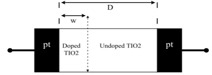
Its prototype is based on a TiO2 thin film containing doped and un-doped regions between two metal contacts at nanometer scale. This implementation, realized by HP researchers, has attracted significant attention. The proposed structure is shown in Figure1 [3].
pt Doped pt
TIO2
Undoped TIO2 w
D
Figure 1: Hewlett Packard original device model.
II.
MEMRISTOR MODELLING
by appertain lower value of current or voltage the foregoing state can be read effortlessly. In 1976 L. Chua and S. Kang generalized the concept of Memristor to a broader class of nonlinear dynamical systems [4]. They called these systems as the memristive systems, the current-controlled, time-invariant Memristor can be reported by the equations as [5].
(1)
(2)
Where w is a set of state variables of the device and f
and R are the clear out functions of time. v and i are voltage and current with respect to time respectively.
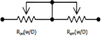
Figure 2: Schematic of the Memristor as proposed by HP Labs
The most common and accepted Memristor model is the Linear ion drift model that is based on the Memristor characteristics described by HP Labs in 2008.In linear ion drift model, a device of physical width D is considered that has two regions viz. dopes and undoped as shown in Figure 2.
A region of width w has high dopants concentration. W
reacts as the state variable of the device. The dopants are oxygen vacancies that are TiO2-x for the case of TiO2 based Memristor. The alternative region of width
D - w is normally an oxide region with the dopant with higher conductance than that of oxide region with mobility of ions is described by .
( ) (3)
(4)
Equations (3) and (4) yields the following equation for state variable w(t) as
(5)
Plugging (fill in)the values from equation (5) into equation (3), we can compute the memristance of the system, for the condition that too reduces to the equation.
( ) (6)
Where, M(q) is the memristance of the memristive system.
To explain the physical behavior of the device, various Memristor models have been suggested. The models proposed are commonly deterministic and commonly do not consider the stochastic switching behavior. The threshold adaptive Memristor model as described in (7) express that the memristors have a current threshold and have an adaptive nonlinearity. For this model, the equation (2) becomes
{
(
)
(
)
(7)
Where and are current threshold parameters and and define the adaptive nonlinearity of device. and, and are the fitting parameters of memristor, and (x) and (x) are the window functions. The voltage of the memristor model v
described in equation (1) can be defined for the threshold adaptive memristor model as per equation (7) as [6]–[8]
(
) (8)
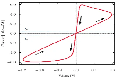
Figure 3: Current–voltage characteristics simulated for TeAM model.
The current-voltage characteristics simulated using TeAM model is shown in Figure 3. I have chosen the TeAM model for its explicit current-voltage relationship and memristance deduction and it shows matching memristive system definition as linear ion drift memristor model shows. This model is more collective and qualified memristive devices [9]. The major characteristic of TeAM model is the existence of threshold because it not only precisely characteristic the Simmons tunneling barrier model but also various different memristor models. The linear ion drift behavior suitable by threshold adaptive memristor model can be given as
(9)
(10)
Linear ion drift memristors does not have any current threshold hence the equation for and
approaches to 0 as
(11)
(12)
(13)
The window function of the TeAM model for the undoped region state variable ≤ x ≤ can be defined as
{ ( )} (14)
Based on the advantage of TeAM model, [10]-[12]‟ have chosen this model for logic design integrated with
CMOS technology. Memristors are compatible with current generation standard CMOS technologies, from the fabrication point of view. The memristors are relatively smaller in size (≈ 3 nm) and thus can be fabricated with the similar techniques used for processing the in-between metal cross-layer via.
Memristors are basically thin oxide sandwiched in metal layers, whereas the oxide shows memristive effect between electrodes. Memristors offer higher density of logic elements per unit area and hence can be used to design much more logic functions on same chip area.
III.
LOGIC USING MEMRISTORS
From the modeling of memristor, it is clear that the memristors exhibit varying resistance when current flows into the device or out of the device the change in resistance with respect to the direction of current flow is shown in the Figure 6. The thick blue line in Memristor symbol represents the polarity of the device.
The basic Boolean logic operations AND and OR can be analyzed using memristors. Although, many researchers have reported the material implication logic using memristor but that is not compatible with current generation CMOS process. Material implication works on the state variable, the inputs and outputs are the states of memristors instead of the voltages that are required for signal propagation in CMOS process. So, to integrate memristor with CMOS and to work with same voltage levels, there is a need of hybrid Memristor – CMOS (MeMOS) logic.
In this logic, the voltages are used as logic state. Memristors can only be used as computational element rather than computational cum storage element as can be used using material implication logic.
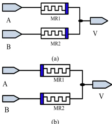
AND gate circuit designed using memristors. We just need to change the polarity of memristors to get the correct logic value. The simulation results are shown in Figure 5.
A
B
V
MR1
MR2
(a)
B
A
V
MR2 MR1
(b)
Figure 4 : (a) Logical AND and (b)OR operation using memristors as voltage divider
(a)
(b)
Figure 5: Simulation results (a) AND and (b) OR gates respectively
Fig.6 describes the computation of AND operation for all input cases of a two input AND gate using memristors only. For case A=1 and B=1, both the inputs are tied to VCC i.e., at logic1. As described in Fig. 6(a), no current flow through the circuit and the output in this case is logic=VCC or 1. For the case of A=0 and B=0 as shown in Fig.6(c) it can be considered that the inputs are at logic0, the output should also be
logic0. Again, there is no current flow through the circuit; the same logic appears at output node V. These two cases are same for OR logic also. Even with the reverse polarity of memristors, the output remains same.
For the case when any of input is at logic 1 and other at logic 0 as shown in Fig. 6(b). In this case, input A=1 and B=0 the current flows through VCC to GND. When current passes from memristor MR1, the resistance of that memristor increases to , the resistance of memristor MR2 decreases to and current leave through GND node. Resistance of memristors are . By this way, we get two resistors and with different values. Thus, as per the voltage divider rule, we get output V=0 that completes the logic for AND gate as per truth table shown in Fig. 6(d). The calculation of output voltage at V for the voltage divider circuit can be determined as
(15)
is significantly higher than we can simplify the equation as
(16)
When the polarity of the memristors MR1 and MR2 is reversed, the circuit behaves as OR gate. For inputs A=0, B=0 and A=1, B=1 the output V get the value 0 and 1 as no current flow through the circuit and the behavior remains same as in the case of AND gate. Fig. 6(d) shows the case when any one of the input is at logic 1 and other at logic 0. Current flows through the VCC towards memristor MR1. As the memristor is in reverse polarity arrangement, the resistance of the memristor decreases to and thus the voltage shows up at output node V=VCC. The output becomes logic1 when any of the input is at logic1. The resistance of the rmemristor MR1 increases to and the condition remains same because these are the fixed values. The output can be determined for OR gate using the voltage divider rule as
A
Figure 6:(a) shows the case when both the inputs are tied to VCC i.e., A=1, and B=1, output is VCC = Logic 1. (b) Represents the case when both the inputs are at logic 0 i.e., A=0 and B=0, the output V=0 is floating and thus no current flows in circuit. (c) Represents the case when any one of the input is at logic 1 and other at logic 0. In this case, current flows from VCC to GND
increasing the resistance of one memristor (MR1) and decreasing the resistance of other memristor (MR2) as shown. ROFF >>RON and thus the output V=0 can be computed using voltage divider rule given in Eq. (8)(d) Current Flow as per Eq. (9) and thus the output V=1
can be computed using voltage divider.
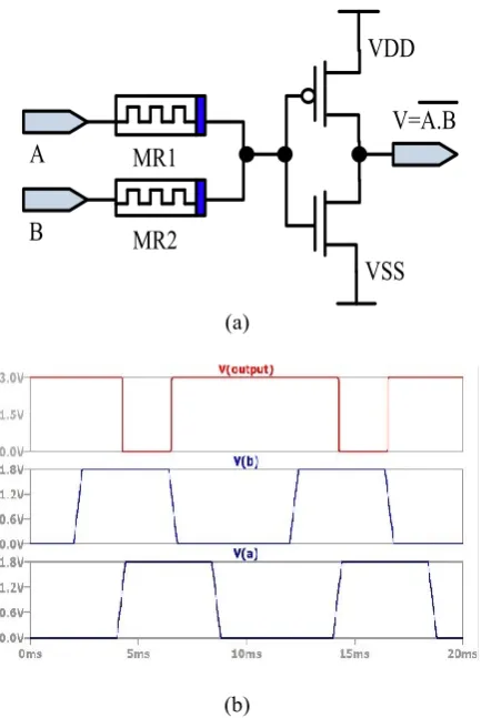
AND and OR gates can be implemented using memristors only. By this apology, even „n‟ input gates can be implemented using memristors. But the primary issue is in complete logic family. Without NOT operation, it is not possible to implement Boolean functions. CMOS inverter can be used to implement NOT operation. The CMOS inverter is designed using 180nm process technology. The operating voltage for the CMOS inverter is 1.8V. We kept the same parameter of memristors as used to simulate the current–voltage characteristics shown in Figure 3. There is an advantage of using hybrid MeMOS logic in terms of level restoration. As per the voltage divider, the output of the memristor based gate depends on the
value of and . Even if there is a large difference in these two values then also the output degrades a little bit as in the denominator term of equation (15) and (17), is added with . In the case of different inputs, I get 0.996 VCC at output. Hence, while cascading memristor stages, the output level decreases. PMOS is always tied to VDD, so when signal pass through inverter, the logic level is retrieved. But in certain cases, we need BUFFER to restore the logic level.
IV.
LOGIC GATES DESIGNING USING MEMOS
Logic
As described in last section, NOT gate
operation is not possible with only memristors. So,
for the complete logic family we should add
CMOS inverter at the output of AND gate to get
NAND operation and similarly NOR operation can
also be implemented. The operating 1.8 voltage is
kept at same level for all the designed gates. The
schematic of NAND or NOR gate (reversed
memristor in this case) is shown in Figure 7.
A
Similarly, XOR gate can be designed using these
approaches as shown in Fig. 8(a). The simulation
results of XOR gate is shown in Fig. 8(b).
V
A
B
v
ccMR2
MR5 MR3 MR1
MR6 MR4 M1 M2
M3 M4
(a)
(b)
Figure 8 :(a) Schematic XOR gate using MeMOS Logic (b) Simulation results for XOR
As designing an XOR gate needs cascaded
stages as shown in the schematic of XOR gate in
Figure 8(a), in this case to restore the level of
output voltages we can use a BUFFER circuits.
After adding the buffer to the level the output is
restore at VCC=1.8v. Although, even in CMOS
process cascading stages need BUFFER for level
restoration but with extra area over head. Any
digital logic circuit can be implemented by using
MeMOS logic can be implemented. I We have
evaluated the analysis of these gates with the
CMOS logic and found that the gates designed
with MeMOS logic shows improved performance
.A. Adder Circuits:
Gates are designed using MeMOS logic. Further
we can extend the circuits towards the basic
building blocks of any computation. i.e adder logic,
adder are plays important role in addition,
subtraction multiplication or division of bits. In
this section reported half adder, full adder, circuits.
Figure 9(a) shows that by adding just two
memristors in the circuit of XOR gate, half adder
can be implemented. In Fig.8(a), memristor MR1
and MR2 completes an AND gate operation that is
same with the memristor MR5 and MR6, while
memristor MR3 and MR4 fulfils an OR gate. Thus,
connecting it in a standard fashion that leads to
XOR gate implementation. From the XOR gate,
we can add one more AND gate at the end of XOR
gate to form half adder as shown in Figure 9 In
this the memristor MR1and MR8 forms AND gate
after the XOR gate to complete the half adder
operation. THE simulation results show in figure
9(b)
.
SUM
A
B
CARRY VDD
MR2
MR5 MR3
MR1
MR6 MR4
MR7
MR8
M1 M2
M3 M4
(a)
(b)
Figure 9: (a) Schematic Half adder using MeMOS Logic (b) Simulation results for half adder
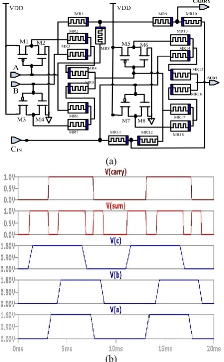
A
Figure 10 : (a) Schematic Full adder using MeMOS Logic (b) simulation results
B. Advantages over Implication Logic
We can perform all logic tasks based on the
memristor IMPLY logic using material implication
[15]. Although, by using this logic we have some
significance advantages like smaller area overhead,
high speed operation and lower power
consumption but IMPLY operation works on only
internal state resistance of memristors. For
external Read/write operations we require current
generation CMOS logic for to convert memristor‟s
state into voltage levels for further computation.
The read/write circuitry consumes much more
power; it leads to overall performance degradation
of the circuit due to bottlenecks of CMOS
technology.
MeMOS logic uses hybrid of both the technologies.
The major advantage of using MeMOS logic is to
integrate the circuits with different circuits
designed by CMOS logic only. Then the
input/output signals work on same voltage level
that is acceptable by CMOS logic, hence the need
of extra circuitry diminishes.
performance analysis of various logic
gates using
MeMOS logic and Table II shows the performance
analysis of gates using CMOS logic.
Table I
Performance Analysis of Logic Gates and Adder Circuits Using Hybrid Memristor-CMOS Logic.
Performance Analysis Of Logic Gates And Adder Circuits Using Cmos Logic Full adder 343.7ps 117.34u
Virtuoso and the performance parameters are
analyzed. The results are acquired for all logic
gates, half adder and full adder. The comparison is
done with current generation CMOS technology.
The parameters of MOSFETs, Memristors and
supply voltages are kept constant for fair
comparison in between these two logic families.
Table III
MOSFET and Memristor Count For Logic Gates
Device N
MOSFET and Memristor Count for Adder Circuits Using Hybrid Memristor-CMOS Logic and CMOS Logic.
Device Half adder Full adder
Hybrid Memristor-CMOS Logic
Memristor 8 18
MOSFETS 8 16
CMOS Logic
MOSFETS 14 34
The extracted performance parameters of various
gates and adder circuits are given in Table I for
respectively. The parameter comparison of adder
circuits with CMOS logic is shown in Table V.
Table V
Comparison of Parameters of Hybrid
Memristor-CMOS Logic with Memristor-CMOS Technology
Parameter Half adder Full adder Area utilization
architectures. The degradation factor using linear
ion drift model is also considered and thus by
using TeAM model. Logic gates are designed with
CMOS 180 nm process technology. Adder circuits
are designed and the performance is analyzed and
compared with current generation CMOS 180nm
technology. This paper opens the possibility of
newly developed memristor for logic circuits.
Based on the excellent performance of adder
circuits, this work can be extended further on
complex logic architectures like multipliers and
many more.
Found” Nature, Vol. 453, pp. 80-83, May 2008. [3]. Mohammad Mahvash and Alice C. Parker "A filter” Circuits and Systems Regular Papers, IEEE Transactions. on, vol.58, no.,pp.1337– 1344, 2011.[5]. O. Kavehei, et al, "Ananalytical approach for memristive nano architectures” Nanotechnology, IEEE Transactions on, vol.11, no.2,2012.
[6]. B. Muthu swamy, P.P. Kokateetal., "Memristor-based chaotic circuits” IETE Technical Review, vol.26, no.6, p.417, 2009.
[7]. J. Nickel, "Memristor materials engineering: From flash replacement towards a universal memory” in Proceeding soft the IEEE IEDM Advanced Memory Technology Workshop, 2011.
notes]” Circuits and Systems Magazine, IEEE,vol. 11, no. 4, pp. 36–44, 2011.
[9]. F. Corinto and A.Ascoli "A boundary condition-based approach to the modelling of memristor nano structures” Circuits and Systems Regular Papers, IEEE Transactions on, vol. 59, no. 11, pp. 2713–2726,November 2012
[10]. S. Kvatinsky, et al, "Memristor-based imply logic design procedure” in Computer Design (ICCD), 2011 IEEE 29th International Conferenceon.IEEE,2011,
[11]. S. Kvatinsky, K. Talisveyberg, D.Fliter,. G.Friedman, A. Kolodny, and U. C. Weiser, "Verilog -a for memristor models” Cite seer, Tech. Rep., 2011.
[12]. S. Kvatinsky, et al, "Models of memristors for spice simulations”, in Electrical & Electronics Engineers in Israel (IEEEI), 2012 IEEE 27th Convention of. IEEE, 2012,
[13]. J. Borghetti, et al, "Memristive switches enable stateful logic operations via material implication” Nature, vol 464,no 7290,pp.873–876,2010. [14]. U. C. Weiser, et al, "MRL-Memristor Ratioed
logic” in International Cellular Nano scale Networks and their Applications, August 2012. [15]. E. G. Friedman, et al, "Memristor based material