Module 19: Output Generation
and CAM File Editing
Module 19: Output Generation and CAM File Editing
19.1
Bill of Materials ... 19-1
19.1.1 Generating a Bill of Materials ...19-1 19.1.2 Using databases with the Bill of Materials...19-2 19.1.3 Setting up the link to a database...19-2 19.1.4 Linking the database to the Bill of Material ...19-4 19.1.5 Adding PCB Information Directly to a BOM ...19-4 19.1.6 Supplier Options...19-5 19.1.7 Exporting the Report ...19-6 19.1.8 Using Excel Templates...19-6
19.2
Output Generation... 19-8
19.2.1 Creating a new Output Job file...19-8 19.2.2 Setting up Print job options ...19-9 19.2.3 Creating CAM files ...19-10 19.2.4 Gerber ...19-11 19.2.5 NC Drill ...19-11 19.2.6 ODB++ Output...19-12 19.2.7 Pick and Place...19-12 19.2.8 Testpoint report ...19-12 19.2.9 Smart PDFs...19-12 19.2.10Publish To Web ...19-13 19.2.11Running the Output Generator...19-18 19.2.12Exercise – adding an OutJob file to the project ...19-18
19.3
CAM Editor... 19-20
19.3.1 Setting up data to use in the CAM Editor ...19-20 19.3.2 Import Data...19-20 19.3.3 Layer Type Assignments...19-21 19.3.4 Board Stackup and Drill Sets ...19-23 19.3.5 Netlist Extract ...19-24 19.3.6 Running a DRC ...19-25 19.3.7 Using Auto Fix ...19-28 19.3.8 Checking Remaining Violations ...19-29
Software, documentation and related materials: Copyright © 2009 Altium Limited.
All rights reserved. You are permitted to print this document provided that (1) the use of such is for personal use only and will not be copied or posted on any network computer or broadcast in any media, and (2) no modifications of the document is made. Unauthorized duplication, in whole or part, of this document by any means, mechanical or electronic, including translation into another language, except for brief excerpts in published reviews, is prohibited without the express written permission of Altium Limited. Unauthorized duplication of this work may also be prohibited by local statute. Violators may be subject to both criminal and civil penalties, including fines and/or imprisonment. Altium, Altium Designer, Board Insight, Design Explorer, DXP, LiveDesign, NanoBoard, NanoTalk, P-CAD, SimCode, Situs, TASKING, and Topological Autorouting and their respective logos are trademarks or registered trademarks of Altium Limited or its subsidiaries. All other registered or
unregistered trademarks referenced herein are the property of their respective owners and no trademark rights to the same are claimed.
19.1 Bill of Materials
19.1.1 Generating a Bill of Materials
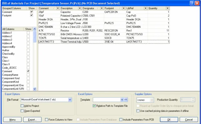
Altium Designer includes a powerful report generation engine, which can be used to generate a comprehensive Bill of Materials.
• Any schematic or PCB component property can be included. For components that link to a company database, database fields that were not included in the schematic can also be included in the BOM. Enable the Show checkbox to include a component property. To include PCB parameters enable the Include Parameters from PCB option, to include additional database parameters enable the Include Parameters from Database option.
• The layout and grouping of data in the report is fully customizable, drag and drop columns to re-order them, drag component properties into the Grouped Columns region to group by that property.
• Supported output formats include: text, CSV, XLS, HTML and XML.
• Excel (XLS) format output can auto load into your company Excel (XLT) spreadsheet.
• Report customization is remembered when you click OK to close the dialog.
• Click Export to generate the BOM in the selected File Format.
• Project and document parameters can also be included in the BOM. For example, to include the value of the project parameter DesignRevision (added in the Project Options dialog) in the exported BOM, add the string Field=DesignRevision to the Excel template.
• The report generation engine can be accessed via the Reports » Bill of Materials menu entry (settings are saved in the project file), or via the Output Job editor (settings are saved in the OutJob file). Choose one approach and use only that approach, since the settings of each are stored separately.
Figure 1. Configuring the layout of the Bill of Materials, then click Export to generate in the selected file format.
19.1.2 Using databases with the Bill of Materials
Using this method, the Database Link file (*.DBlink) defines linkage between the schematic component and a matched record in a database. The record match is established by key field linking, which can be a single key field (for example a part number), or multiple key fields (by defining a Where clause).
With this method of linking, the model and parameter information for the component must be predefined as part of the Altium Designer library component. The library component must also include the necessary key field information as part of its definition. Once this has been defined you add a database Link document (*.DBlink) to your Library Package or PCB project, then you can synchronize the component information (parameters) with the contents of fields in the database.
Although each physical component defined by each database record does not need to map to a unique Altium Designer library component – many database components can share the same component symbol – this method of linking would typically be used in a "one database record-to-one Altium Designer comprecord-to-onent" fashion. The unique Altium Designer comprecord-to-onent can either be an instance placed on a schematic sheet, or a unique component in a component library. With DBLink-style database linking, you include the Database Link file with the project.
19.1.3 Setting up the link to a database
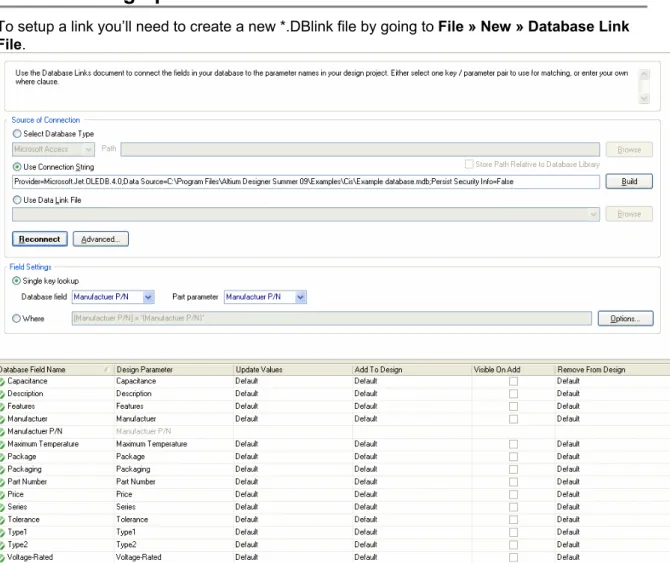
To setup a link you’ll need to create a new *.DBlink file by going to File » New » Database Link File.
The first step is linking to the database itself.
Figure 3. The database link setup.
Figure 3
All Different types of databases can be linked to, including Excel, Access, SQL, MYSQL and even Oracle. Any database which provides OLE DB support can be connected to. In an ODBC based connection string has been built using a datalink direct to an access database.
For more details on all different types of connections to databases refer to the document AP0133 Using Components Directly from Your Company Database.PDF which you can find in the help directory of the Altium Designer installation, or on the Altium website.
The next step is specifying a matching criteria.
Figure 4. The matching criteria
In Figure 4 the criteria is set to Manufacturer P/N for both database field and the part parameter field. This means there needs to exist this parameter in both the database and on a created component were the original component came from, be that a schlib, integrated library or a database library. This field has to be a unique field that exists in both the database and on the components being linked to.
Once the look up key is set, there is also the field mapping to be setup.
The first two columns (from the left) on the Field Mappings tab allow you to control which information from the database is to be mapped to the component's models and parameters.
The Database Field Name column lists all field (column) names in the currently active table of
the database. The Design Parameter column defines how each corresponding field in the database is to be used – whether it is used to source a schematic component, link-in a particular model, or to be attached to the component as a mapped design parameter.
Initial mapping is performed automatically upon connection to the database, with all database fields mapped.
For fields that you explicitly do not want mapped from the database, set the Design Parameter
entry to [None]. Unmapped database fields are distinguished on the tab by the use of a red cross icon . Mapped database fields are distinguished by a green tick icon .
19.1.4 Linking the database to the Bill of Material
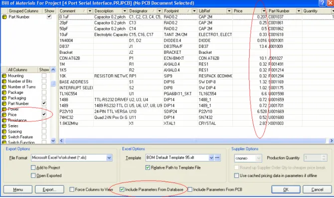
Source information for a Bill of Materials (BOM) has, in the past, been taken from the parameter information of the placed components for the design. But that can lead to a lot of information attached to a schematic that is only ever used for the BOM. If you place components from a Database Library the BOM Generator is able to extract any other record information that has not been added as design parameters at the time of placement.
When configuring the Bill of Materials report using the Report Manager, simply enable the
Include Parameters from Database option. This option will only be available if one or more
components in your design are linked to an external database. In the parameter listing, the icon is used to distinguish a parameter that exists for one or more placed components in a linked external database.
Figure 6. Include additional component information that exists only in an external database
19.1.5 Adding PCB Information Directly to a BOM
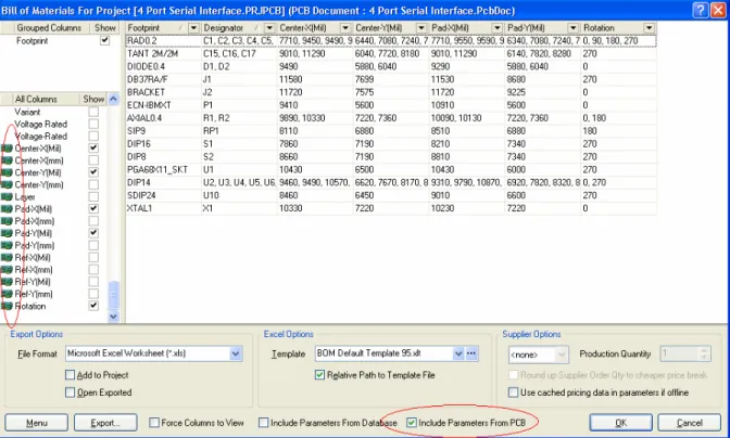
Source information for a Bill of Materials (BOM) can be based on property information taken from the PCB in the event you need to customize and use the report generation for more than a BOM.
An example would be for generation of a pick and place file where every placement machine wants the data (such as X, Y location) in a different column order and in different file formats. When configuring the Bill of Materials report using the Report Manager dialog, simply enable the
Include Parameters From PCB option. This option will only be available if there is a PCB
document in the project file. In the parameter listing, the icon is used to distinguish a PCB parameter for one or more placed components in the project.
Note that when you have a project with multiple PCBs and you enable the Include Parameters
From PCB option, the BOM Report Options dialog will automatically prompt you to select which
PCB toinclude in the BOM report.
Figure 7. Include additional component information that exists in a PCB.
19.1.6 Supplier Options
This feature located in the bottom right side of the bill of materials dialog enables the use of linking to direct supplier data that is already embedded in the design from suppliers such as Digikey, Farnell and Newark. In order for this section to function certain parameter need to exist in the design.
• Supplier Unit Price
Once this parameter has been enabled in the left column the supplier options should fully enable.
Figure 8. Supplier options in the bill of materials.
From here the local currency can be picked. There is two further options to pick, round up
supplier order Qty to cheaper price break. This tick box should pick the cheapest option for
buying the extra is cheaper than the bill of material should round up to cheaper price point. The second option, use cached pricing data in the parameters if offline is useful if the design in progress uses a database library or you are offline, then it’ll use the data that is already cached in the design, using the conversion rate done at the time of population of the parameter in the design.
Note: The currency data is set in the pricing parameter. If there is a difference between the
pricing data currency and local currency a conversion takes place.
19.1.7 Exporting the Report
The grid content of the data section can be exported and a report generated by using the Export
button in the Report Manager dialog.
1. Select a File Format from the drop-down list. When exporting the data using the Export
option from the Report Manager dialog, the following file formats are supported:
- CSV (Comma Delimited) (*.csv)
- Microsoft Excel Worksheet (*.xls)
- Tab Delimited Text (*.txt)
- Web Page (*.htm; *.html)
- XML Spreadsheet (*.xml).
2. If you want the relevant software application, e.g. Microsoft Excel, to open once the exported file has been saved, make sure the Open Exported option is enabled in the Report Manager dialog.
3. If you want to have the generated report added to the project after it is created, simply enable
the Add to Project option in the Report Manager dialog.
4. Click on Export button in the Report Manager dialog and to generate and save the report in the appropriate format.
19.1.8 Using Excel Templates
If you want to export your data straight into an Excel template, you can select an existing Excel template or you can use the supplied Excel templates.
1. If the Microsoft Excel Worksheet (*.xls) file format is selected, the Template field becomes available in the Excel Options region of the Report Manager dialog. Enter the required Excel template file (*.XLT) directly into this field, or browse for it by clicking the ... button. The field's drop-down list contains a range of default templates for the installation.
Select the BOM Default Template.XLT from the \Program Files\Altium Designer Summer 09\Templates folder. The file can be specified with a relative or absolute path using
the Relative Path to Template File option. For more information about template creation, refer to
your Microsoft Excel documentation.
Figure 9. File format and template data set for Bill of Materials.
2. If you have the Open Exported option selected in the Report Manager dialog, the file will open in Excel after export.
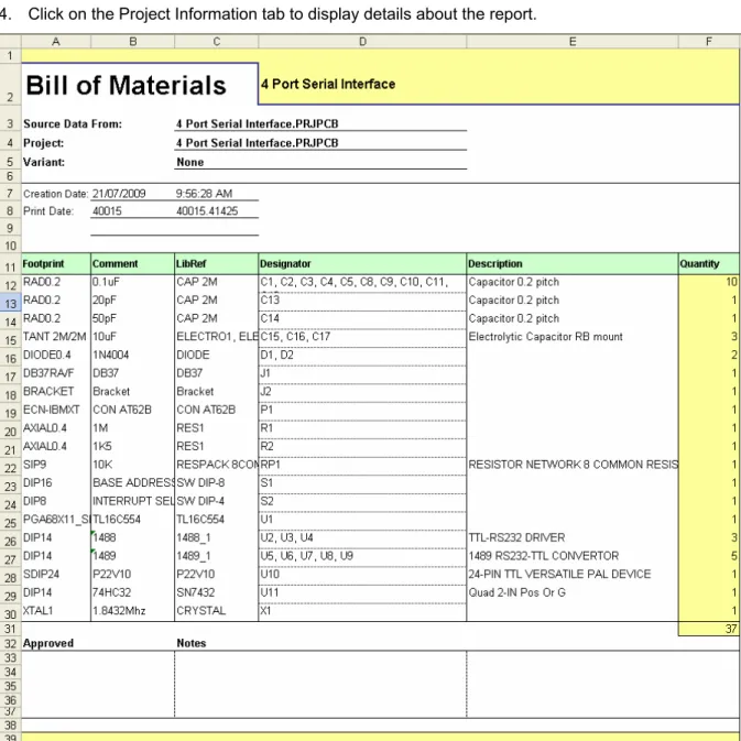
3. Click on the Export button and nominate a filename and location for your report and click on
4. Click on the Project Information tab to display details about the report.
19.2 Output Generation
All output generation settings (print, Gerber, NC drill, ODB++, CAM, report and netlist, etc) can either be:
•
•
19.2.1
Configured and stored as part of the project. If you select print, Gerber, and other outputs from the PCB editor’s File, Design and Reports menu these output configurations are stored in the project file.
Alternatively you can add an Output Job file to the project and store the output setups there. The advantage of an Output Job file is that it supports setting up multiple outputs of any kind. It also allows multiple outputs to be generated in a single operation, and the OutJob file can be copied from one project to another. Any combination of output setups can be included in the OutJob file, and any number of OutJob files can be included in the project. Note that setting made in the OutJob file are completely independent of the settings made in the PCB Editor’s menus.
Creating a new Output Job file
The Output Job file enables you to define all of your design output configurations - assembly, fabrication, reports, netlists, etc - all in the one convenient and portable file. Each output setup uses a specific data source including the entire project (all schematic sheets), an individual schematic or the PCB.
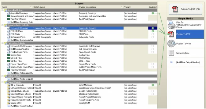
• Select File » New » Output Job File to create a new output job configuration file. A new output job configuration file (Job1.OutJob) is created and added to the Job Files sub-folder of the focused project in the Projects panel. It opens as the active document in the design window and defaults to include all possible output setups.
Figure 11. A Output Job file with four output setups configured to be published into the one PDF fle.
•
•
Selected setups can be deleted (CTRL+A to select all) and new outputs can be added at any time by clicking on the required Add New Output.
Double-click on an output to configure it in its Properties dialog, or right-click for a list of options. The Data Source and Variants columns also have a drop-down list to choose from —
click once to select the item, then click a second time to display the down arrow and then select from the list.
19.2.2 Setting up Print job options
• Select a print output from the Output Job file, e.g. Composite Drawing. Double-click to configure this printout option in the PCB Printout Properties dialog.
Figure 12. Printout Properties dialog
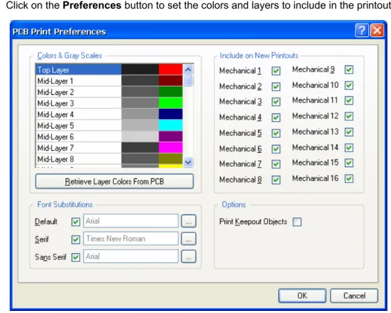
Click on the Preferences button to set the colors and layers to include in the printout.
•
Figure 13. PCB Print Preferences dialog
•
•
Right-click on the print option in the Output Job file to configure which printer your output will print to (Printer Setup) as the printouts will be sent directly to that printer when you run the output generator.
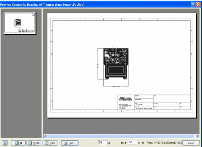
Right-click and select Print Preview to view your printout. From the preview window you can copy the current Printout preview to the Windows clipboard by right-clicking and selecting
Copy. You can also save the image as an Enhanced Windows Metafile (.emf) by right-clicking and selecting Export Metafile.
Figure 14. Print Preview window with all layers displayed.
•
19.2.3
When the printout is configured, you can run it as a batch job (if Batch is enabled) along with all the other setups (F9), run the current output generator (SHIFT+F9) or run a selection of output generators (CTRL+SHIFT+F9). These output options are also available in the right-click menu. The printouts are sent to the printer.
Creating CAM files
You can setup and create manufacturing output files from the Output Job file, such as:
• • • • • Bill of Materials
Gerber and ODB++ files NC Drill files
Pick and Place files Testpoint Report.
The data is output into appropriate documents in a folder within the same folder as your PCB file or in separate folders for each output type as determined in the Options tab of the Options for Project dialog.
19.2.4 Gerber
This option in the Job Output file produces a Photoplotter output in Gerber format. Double-clicking on a Gerber Files output displays the Gerber Setup dialog. Consult your PCB manufacturer for their preferred settings.
Figure 15. Gerber Setup dialog
19.2.5 NC Drill
This option produces a NC drill output in an industry standard format. Double-clicking on NC
Drill Files displays the NC Drill
Setup dialog. Consult your PCB manufacturer for their preferred settings.
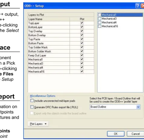
19.2.6 ODB++ Output
This option produces ODB++ output, ready to load into any ODB++ compliant CAM tool. Double-clickingon ODB++ Files displays the Select
Layers to Plot dialog.
19.2.7 Pick and Place
This option produces component data that is used to program a Pick and Place machine. Double-clickingon Generates Pick & Place Files
displays the Pick and Place Setup dialog.
19.2.8 Testpoint report
This option produces information on the location and size of Testpoints for use in fabricating test fixtures and programming testers.Double-clicking on a Testpoints
Reports displays the Testpoint
Report Setup dialog.
19.2.9 Smart PDFs
Altium Designer has built in PDF generation capabilities. As well as being able to create standard PDF files showing the schematic sheets and the PCB layers, you can also include linked PDF bookmarks to components and nets on the sheets and board.
There is 2 ways of generating PDFs, select File» SmartPDF from the schematic or PCB editor menus, or use the Publish To PDF option in the Output Job editor.
Using the SmartPDF wizard creates an output job file at the end of the process with all the options that were specified in the wizard. This is a handy tool if you are not too familiar with the output job file and how to modify the setups.
19.2.10 Publish To Web
The main role of the new web publisher output medium is to enhance collaboration by making web publication of design outputs (graphical and table based) easy and automatable.
The new web publisher will publish the outputs of Outjob Documents on web hosted media (FTP, S3, WebDav) as well as locally.
19.2.10.1 Locating
From the File menu, select New»Output Job File.
Click on the Publish To Web output medium, and select the outputs you wish to publish by clicking in the Enabled column. A green arrow leading to the output medium will appear for each output selected.
Figure 19. Publish to web in the output job file
19.2.10.2 Settings Window
Once the desired outputs have been selected, right click on the output medium Publish To Web
and select Web Setup.
The settings window will display and allow you to configure the web output destination.
19.2.10.3 Prompt if files already exist
When selected this option will cause the system to confirm with you before overwriting any files in the destination.
19.2.10.4 Open after export
When selected this option will cause the system to open the published files in a web browser window.
19.2.10.5 Destination Type
Four destination types, each representing a different way of transferring files, are available allowing you to select the method best suited to your environment.
19.2.10.6 Destination Type - File System
The file system destination type will publish the web output to a folder of your choosing, either on your local machine, or on a shared network drive.
19.2.10.7 Output Folder
This is the folder where the published files should be placed.
Figure 20. File system and destination options
19.2.10.8 Destination Type - FTP
The FTP destination type will publish the web output to a server capable of accepting files via the File Transfer Protocol (FTP).
19.2.10.9 Server Name
The server name or address used to identify the server on the network.
19.2.10.10 User Name
The account on the server with the appropriate upload permissions.
19.2.10.11 Password
19.2.10.12 Output Folder
The folder into which the files should be placed on the server.
19.2.10.13 HTTP URL
The URL which can be used to access the folder in a standard web browser. If blank the web browser window will not be opened at the completion of the transfer.
Figure 21. FTP destination options
19.2.10.14 Destination Type - WebDAV
The WebDAV destination type will publish the web output to a web server capable of accepting files via the WebDAV protocol.
19.2.10.15 URL
The full URL of the destination, including both the server name and the output folder.
19.2.10.16 User Name
The account on the server with the appropriate upload permissions.
19.2.10.17 Password
Figure 22. WebDEV destination options
19.2.10.18 Destination Type - S3
The S3 destination type will publish the web output to Amazon's Simple Storage System (S3). An account with Amazon is required for this destination type.
19.2.10.19 Account Name
Your Amazon account name.
19.2.10.20 Access Key
Your Amazon access key.
19.2.10.21 Secret Key
Your Amazon secret key.
19.2.10.22 Bucket
The bucket into which the files should be uploaded.
19.2.10.23 Key Prefix
The prefix to add to each file name. A key prefix ending with / will cause the files to be placed in a folder with the key name.
Figure 23. Amazon S3 destination options
19.2.10.24 Publish
Once the settings have been confirmed you may click the Publish To Web button to start the upload. Once the upload has completed a web browser will open and display the published files.
Figure 24. Final result publish to web
19.2.11 Running the Output Generator
You can run the Output Generator to create your output files and printouts from within the Output Job file itself (right-click menu) or use the Tools menu which includes a number of Run options. When the Run Batch command is selected (F9) all output setups with the Batch checkbox ticked will be generated.
You can also generate output for a selected group of outputs from within the Output Job file by highlighting them and selecting the Run Selected command (SHIFT+CTRL+F9).
Fabrication CAM outputs can be set to open automatically in CAMtastic by enabling the relevant options in the Output Job Options dialog (Tools » Output Job Options).
19.2.12 Exercise – adding an OutJob file to the project
1. With the Temperature Sensor project open, select File » New » Output Job File. 2. Save the document, naming it as Temperature Sensor.OutJob.3. Select all the output setups (CTRL+A), and press Delete to remove them. 4. Add in an Assembly Drawing, Gerber, NC Drill and a Bill of Materials.
5. Click on the Gerber output setup to select it, then right click and configure the output. Make sure layers are ticked, format set correctly, apertures etc… Do the same for the NC drill output.
7. In the Output Job Options dialog, enable the Gerber and NC drill output check boxes and close the dialog.
8. Select both the Gerber and NC drill using the ctrl key, right-click and choose Run Selected
from the menu. The files will be generated, a new CAMtastic document created and the gerber and NC drill documents loaded into it. These can now be checked, panelized, and so on.
9. Once the Gerber is created, go back into the output job file and create a PDF of the assembly drawing using the publish to PDF output type.
19.3 CAM Editor
Altium Designer’s CAM Editor (CAMtastic) offers a variety of tools, the most basic of which are for viewing and editing CAM data. Once image and drill files have been imported, the Editor can receive instructions determining layer types and stackup, at which point a netlist can be extracted and compared with an IPC netlist generated from the original PCB design software. These netlists will handle not just through-hole components, but blind and buried vias as well. The Editor also offers Design Rule Checking, panelization and NC-Routing (plus milling) tools.
19.3.1 Setting up data to use in the CAM Editor
• After importing CAM data into a CAMtastic document, you may notice that there is options grayed-out, like export to PCB and DRC doesn’t work.
• The following sections detail steps to be taken in order to get Gerber or ODB++ data ready to use in a CAMtastic document.
19.3.2 Import Data
• The starting point for the whole process is the loading of ODB++, or Gerber and NC Drill files, into a new CAMtastic document. If you have an IPC netlist, you should import this as well when importing Gerber and NC Drill data. When importing ODB++, only import an IPC file if the netlist is not in the ODB++ directory. The IPC netlist will allow you to update the extracted nets with their original names, and differentiate between through-hole vias and free (non-component) pads.
• The File » Import submenu commands all search for files with certain extensions within a given folder. When importing drill files, for instance, the specified directory will filter out all files except those with .DR*, .ROU, .RTE, .NC* and .TX* extensions. If you receive dfiles with different extensions than these, you may extend this list on the CAMtastic – Miscellaneous
page of the Preferences dialog (DXP » Preferences).
• From here you can alter any of the default extension lists associated with Gerber, Aperture, HPGL and Netlist files as well.
• The CAMtastic – Import/Export page of the Preferences dialog lets you change the default import and export settings for Gerber files. For example, if you regularly receive CAM data generated using P-CAD, you might consider changing the coordinate precision format from 2:3 (Altium Designer defaults) to 4:4 (P-CAD defaults). If you don’t you will still have the opportunity to change these settings from their default state each time you import a job.
Figure 26. Import/export options in preferences for CAMtastic.
19.3.3 Layer Type Assignments
• Individual Gerber and Drill files are all assigned to individual layers. In addition, the CAMtastic Editor looks at their names upon import, and tries to assign each one a layer type. It does this according to the information in the Layer Types Detection Template dialog (Tables » Layer
Type Detection). This is a fully-customizable dialog that contains fragments of file names
(extensions, keywords or both) that identify individual files as layer types, such as signal, negative plane, border, drill, and temporary layers (mechanical).
• Altium Designer’s PCB Editor, for example, differentiates between Gerber layers by their extensions, such as .gtl for the top layer and .gbl for the bottom. Other design programs might export a .top file for a top layer, and a .sol file for the bottom (solder) layer. Some of these programs, such as P-CAD, allow users to specify the Gerber output names
themselves.
• After importing any group of CAM files, you should open the Layers Table dialog and review the type assignments that have taken place automatically.
Figure 27. Layer types detection setup.
• You may open the drop-down list for the type and modify any assignment. For example, you will notice that all drill files are automatically set to type Drill Top. You might want to distinguish between top, bottom and internal drill sets at this point. This is not required, however. Later on we’ll discuss pairing layers to accommodate boards containing blind and/or buried vias.
• If you customarily receive Gerber or drill files that are not automatically assigned to a layer type correctly, you should look over the file name fany distinguishing characteristics whereby the CAMtastic Editor might identify them, and add them to the Layer Types Detection
Template dialog.
• ODB++ does not need to use the Layer Types Detection Template dialog because all the information needed to identify each layer is stored in the matrix file. However, it is good practice to check the layer type assignments after the loading process ends.
Figure 28.Layers table assigning Gerber layers to Camtastic layers.
19.3.4 Board Stackup and Drill Sets
• Layers that have been assigned as signal types (top, bottom or internal) or planes will now appear in the Create/Update Layers Order dialog (Tables » Layers Order). In most cases, the CAMtastic Editor will be able to determine the stackup from the provided CAM data, but in some cases all that will be provided is the logical order (the order in which the layers were imported). It is your responsibility to make sure that the information in the Layer Physical Order column is correct, with number one being the top layer. Be careful not to assign the same order number to different layers. Once you have specified a valid stackup, the physical order column will take precedence over the logical list when this dialog is reopened and you will see the layers listed in their proposed stackup.
• This same physical order will be reflected in the Create/Update Layers Sets dialog (Tables »
Layers Sets), where you match drill files to layer sets. Consider a 6-layer board (four-signal,
two-plane) with both blind and buried vias. The design might contain four separate drill files:
- one for the Top-Bottom pair (thru-holes)
- one for the Top-InternalPlane1 pair
- one for the MidLayer1-MidLayer2 pair
- one for the Bottom-InternalPlane2 pair.
• Remember that you are determining a drill set, not just outermost pairs. For blind/buried drill layers, all layers that are drilled need to be in the layers set. For through hole drill layers, the start and end layers should suffice.
Figure 30. Drill setup for thru hole and blind and buried setups.
19.3.5 Netlist Extract
• This step (Tools » Netlist » Extract) relies on the accuracy of the steps preceding it. You can’t do it at all unless you’ve got a layer type assignment for every layer in your board (you should set mechanical layers to Temporary).
• The CAMtastic Editor will trace connectivity from one layer to another, consulting the NC drill files to make layer to layer connections. For this reason, the layer stackup you defined in the Create/Update Layers Order dialog, and the drill pairs you selected in the Create/Update Layers Sets dialog, are critical precursors to extracting an accurate netlist from the CAM data.
• If you have included an IPC netlist file with your imported Gerber and NC Drill files, you may restore the original net names (Tools » Netlist » Rename Nets) and differentiate between through-hole vias and free pads in your new PCB file. But much more importantly, an IPC netlist gives you a reference with which the extracted netlist can be compared (Tools »
Netlist » Compare).
• For IPC netlists generated from Altium Designer’s PCB Editor, you will notice that the
CAMtastic Editor’s compare function will usually find a series of “missing nets” without names. This is because the PCB Editor’s IPC format includes single-pin nets – the CAMtastic Editor, on the other hand, disregards pads without any copper connections as far as the netlist is concerned. In fact, its DRC has an option to remove non-functional pads.
19.3.6 Running a DRC
• Now we can run a DRC (Design Rule Check) to verify there are no violations in your CAM file that will affect the fabrication. You are presented with 18 rules. The values for these rules will be retained from your previous CAMtastic sessions, unless you loaded your CAM data from a Protel output that included a .RUL file. In any case, the values of these rules may be modified before running the DRC.
19.3.6.1 Setting up the DRC
1. Select Analysis » PCB Design Check/Fix. The PCB Design Check/Fix dialog displays.
Figure 31. DRC setup in Camtastic.
2. From this dialog, you can change relevant size values, if required, or enable the Auto Fix option, if available, so CAMtastic will attempt to fix any violations found. We will first run the DRC without Auto Fix enabled to review the number of violations and then with an Auto Fix option enabled. Type in the sizes as displayed in the PCB Design Check/Fix dialog above. Enable all the Check column boxes. You can click on the Check header to toggle all options on or off.
3. Once you have set up the DRC, you can save the DRC settings to a .DRC file by clicking on
Save. Use the Open button to reload saved .DRC files.
Figure 32. Results of a DRC check in Camtastic.
5. Click OK to close the dialog and click on the Drc tab in the CAMtastic panel to view more details about each of the violations.
Figure 33. Navigation of DRC violation in the Camtastic Panel.
6. Double-click on a violation error folder in the Drc tab of the CAMtastic panel, e.g. Silkscreen over Solder mask, to view the individual error subfolders. Click on a subfolder, e.g. Ref (13), to zoom in on and highlight the offending object/s in the design window.
Figure 34. A Silkscreen over soldermask problem found in CAMtastic.
19.3.6.2 Querying a violation for further information
You can find out more information about the possible reason for errors by querying the object/s involved in the violation.
Figure 35. Query results in CAMtastic. 1. If the CAMtastic panel is active, press Shift+F5 to
make the design window active, or click in the workspace. You can now use the zoom and pan commands.
2. Press Q for Query (or select Analysis » Query » Object) and the cursor changes to a pointing hand. Click on the object you wish to find more information about. The information about the selected object is displayed in the Info tab of the CAMtastic panel. At the bottom of the Info Query section, all the DRC errors are listed that relate to the queried object. Click on these errors to zoom into those related violations.
3. You may also wish to measure distances between objects if there are clearance issues. Select a measuring option, such as Point to Point or Object to Object from the Analysis » Measure submenu and click on the points or objects you want to measure. The measurements are displayed in the Info tab of the CAMtastic panel.
19.3.7 Using Auto Fix
1. In the PCB DesignCheck/Fix dialog (Analysis
» PCB Design Check/Fix),
enable all items in the Check column. Enable the Auto Fix checkbox for the Silkscreen over Solder Mask design rule only. Click OK to rerun the DRC. The
CAMDXP dialog displays the results.
Figure 36. Summary of the fixes made in CAMtastic. 2. You will notice that number
of violations has been reduced as the Auto Fix option has resolved the Silkscreen over Solder Mask
errors. Auto Fix removes enough of the overlaid object to clear the violations.
3. Check what has been achieved by using the Auto Fix option. Double-click on the Silkscreen over Solder mask violation error folder in the Drc tab of the CAMtastic panel, then click on the Ref(13) subfolder to display and highlight the auto fixed objects in the design window.
Figure 37. Fixed problems on the result of the fix on the left.
4. Remember you can always use Edit » Undo
(shortcut Ctrl+Z) to reverse any auto fixes.
19.3.7.1 Using Auto Fix in the CAMtastic Panel
You can also use the Auto Fix option (where applicable) from the right-click menu when in the DRC tab of the CAMtastic panel. This allows you to fix individual errors as well as entire DRC types.
To auto fix all the Silkscreen over Solder Mask errors, for example, from the DRC tab, right-click on the Silkscreen over Solder Mask violations folder in DRC tab of the CAMtastic panel and select
Fix All - Silkscreen over Solder Mask errors. All violations in that folder are fixed.
To auto fix individual errors, right-click on an individual error Ref folder and select Fix DRC Error. The error is fixed.
19.3.8 Checking Remaining Violations
Check the remaining violations and resolve any other errors as necessary. The table below explains the reasons for the remaining violations.
DRC Violations Notes
Annular Ring (Drill>Mask)
The three violations are for annular rings (drill to mask) that have a negative value, which is not interpreted by the DRC. Investigation using the Analysis » Query » Object command (shortcut Q) will show that the drill holes are larger than the pads and have a diameter of 140 mil and the masks are 150 mil in diameter. The drill to mask expansion of 5 mil (half of the difference between the drill hole and mask diameters) is still better than the fab house minimum of 4 mil (pad to mask), so these errors can be ignored.
Solder Bridging
Solder bridging checks the Top and Bottom layers against the Mask Top and Mask Bottom layers for the distance from the edge of the mask opening to any objects under the mask but on a different net from the pad exposed by the mask opening. DRC flags a violation if the nets are different and the objects are not correctly covered by the mask.
In this example, the solder bridging occurs where the routing to the end connector comes in contact with the mask. Since there are many different nets under the mask, errors are generated. Visual inspection shows that this is OK, so the violations could be ignored.
Net Antennas
A rogue flash has been detected. This DRC looks for track ends not terminating on a track end, pad or via. This trace can be deleted by selecting Edit » Clear and then selecting the flash, right-click to Clear and press ESC to end the command. Notify the PCB designer of this alteration.
Table 1. Summary of DRC violations and what they mean.
The data in the design has now been verified and the files are ready for the next stage of fabrication.