Informatics Engineering Degree
Computer Engineering Specialization
Behavior characterization of the
shared last-level cache in a chip
multiprocessor
Author:
Pedro Benedicte
Directors:
Jose Maria Llaberia
Computer Architecture DepartmentTeresa Monreal
Computer Architecture DepartmentAbstract
Since the stop in the frequency increase in processors, chip multiprocessors have become more relevant. A key aspect of chip multiprocessors is their mem-ory hierarchy, specifically the shared last-level cache.
This project consists in analyzing different aspects of the memory hierar-chy and understanding its influence in the overall system performance. The aspects that will be analyzed are cache replacement algorithms, memory map-ping schemes and memory page policies.
Abstract
Desde que la frecuencia en los procesadores dej´o de incrementar, los chips multiprocesador han ganado relevancia. Un aspecto clave de los chips multi-procesador es la jerarqu´ıa de memoria, espec´ıficamente el ´ultimo nivel de cache compartida.
Este proyecto consiste en analizar diferentes aspectos de la jerarqu´ıa de memoria y entender su influencia en el rendimiento del sistema. Los aspectos que se analizaran son los algoritmos de reemplazo, los esquemas de mapeo de memoria y las pol´ıticas de p´agina de memoria.
Abstract
Des que la freq¨u`encia als processadors va deixar d’incrementar, els chips multiprocessador han guanyat rellev`ancia. Un aspecte clau dels chips multi-processador ´es la jerarquia de mem`oria, espec´ıficament a l’´ultim nivell de la cache compartida.
Aquest projecte consisteix a analitzar diferents aspectes de la jerarquia de mem`oria i entendre la seva influ`encia al rendiment del sistema. Els aspectes que s’analitzaran s´on els algorismes de reempla¸cament, els esquemes de mapeig de mem`oria i les pol´ıtiques de p`agina de mem`oria.
Contents
List of Figures 6
List of Tables 8
1 State of the Art 9
1.1 Cache memory hierarchy . . . 9
1.2 Chip multiprocessors . . . 9
1.3 Replacement algorithms . . . 11
2 Replacement algorithms 12 2.1 Least Recently Used . . . 12
2.2 Non Recently Used . . . 13
2.3 Least Recently Reused . . . 15
2.4 Non Recently Reused . . . 18
2.5 Static Re-Reference Interval Prediction . . . 20
2.6 Set Dueling . . . 22
2.7 Dynamic Re-Reference Interval Prediction . . . 22
2.8 Dynamic Re-Reference Interval Prediction with Protection . . . 23
2.9 Thread-Aware Dynamic Re-Reference Interval Prediction . . . 23
3 Simulation 24 3.1 Simulator . . . 24 3.1.1 SIMICS . . . 24 3.1.2 GEMS: Ruby . . . 24 3.1.3 DRAMSim2 . . . 24 3.2 Simulated system . . . 25
3.2.1 Caches and DRAM specification . . . 25
3.2.2 DRAM mapping and page policy . . . 26
3.3 Benchmarks . . . 27
4 Results 29 4.1 Replacement algorithms . . . 29
4.1.1 Performance . . . 29
4.2 Page policy . . . 32
4.3 Mapping scheme . . . 33
5 Project description and planning 35 5.1 Project description . . . 35 5.1.1 Objectives . . . 35 5.1.2 Risks . . . 35 5.1.3 Methodology . . . 36 5.1.4 Tools . . . 36 5.2 Temporal planning . . . 37
5.2.1 Estimated project duration . . . 37
5.2.2 Project tasks . . . 37
5.2.3 Task estimated time and dependencies . . . 40
5.2.4 Gantt chart . . . 41 5.2.5 Action plan . . . 42 5.2.6 Validation method . . . 42 5.3 Project budget . . . 42 5.3.1 Budget justification . . . 42 5.3.2 Human resources . . . 42 5.3.3 Software resources . . . 43 5.3.4 Hardware resources . . . 43 5.3.5 Total budget . . . 44 5.4 Sustainability . . . 44 5.4.1 Social impact . . . 44 5.4.2 Environmental impact . . . 44 Appendices 45 A Cache coherence protocol 47 A.1 High level description . . . 47
A.1.1 Protocol . . . 47
A.1.2 Events . . . 48
A.2.2 Requests . . . 50
A.2.3 States . . . 52
A.2.4 State diagrams and transitions . . . 52
B DRAM behavior 56 B.1 Memory system . . . 56 B.2 DRAM states . . . 59 B.3 Temporal constraints . . . 60 B.4 Energy consumption . . . 63 B.4.1 ACTIVATE-PRECHARGE . . . 63
B.4.2 READ and WRITE . . . 64
B.4.3 REFRESH . . . 65
Glossary 68
List of Figures
1 Cache hierarchy . . . 9
2 Frequency in Intel microprocessors . . . 10
3 Cache hierarchy in a chip multiprocessor . . . 10
4 LRU algorithm . . . 12 5 LRU example . . . 13 6 NRU algorithm . . . 14 7 NRU example . . . 15 8 LRR groups . . . 16 9 LRR algorithm . . . 17 10 LRR example . . . 18 11 NRR algorithm . . . 19 12 NRR example . . . 20 13 SRRIP algorithm . . . 21 14 SRRIP example . . . 21 15 Set Dueling . . . 22
16 Simulation tools used . . . 25
17 Simulated system . . . 25
18 L3 mapping . . . 26
19 DRAM mapping . . . 27
20 Performance of the different replacement algorithms over LRU . . . . 30
21 Relation between the performance and the misses of DRRIP . . . 30
22 Miss distribution by L3 bank . . . 31
23 DRAM energy reduction over LRU . . . 32
24 CPI and MPKI with Open Page . . . 33
25 CPI and MPKI with Close Page . . . 33
26 CPI and MPKI with Mapping 1 . . . 34
27 CPI and MPKI with Mapping 2 . . . 34
28 Gantt chart . . . 41
29 Memory hierarchy description . . . 47
34 PUTS and PUTX transitions . . . 55
35 DRAM DIMMs . . . 56
36 DRAM banks . . . 57
37 DRAM arrays . . . 58
38 DRAM cell . . . 59
39 DRAM states and transitions . . . 60
40 ACTIVATE-PRECHARGE current through time . . . 63
List of Tables
1 Cache and DRAM characteristics . . . 26
2 Benchmarks . . . 28
3 Task estimated time and dependencies . . . 40
4 Human resources costs . . . 43
5 Hardware resources costs . . . 43
6 Total costs . . . 44
7 L2 to L3 requests . . . 50
8 L2 requests and L3 replies . . . 51
9 Directory requests to L2 . . . 51
10 Directory requests and L2 replies . . . 51
11 L3 stable states . . . 52
12 L3 transient states . . . 52
13 DRAM commands . . . 59
14 DRAM states . . . 59
15 DRAM latencies . . . 61
16 DRAM same bank accesses delays . . . 62
17 DRAM different bank same rank accesses delays . . . 62
1
State of the Art
1.1
Cache memory hierarchy
One of the main issues in computer architecture is the time it takes to transfer an element from the memory to the processor. This happens because the memory access time is directly proportional to its size [1], so big memories will be slow, and fast memories will be small.
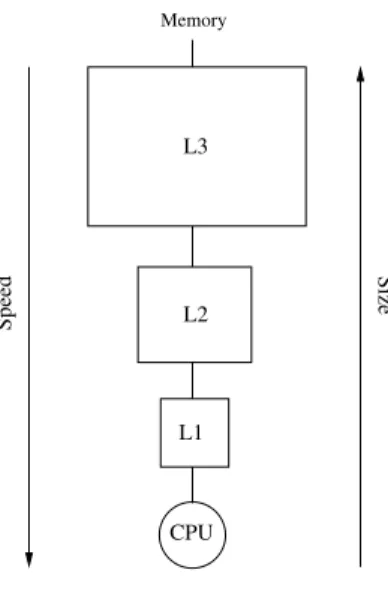
This issue has been mitigated with the usage of caches. A cache is a small memory that takes advantage of spatial and temporal locality in order to reduce the number of accesses to memory, and thus the latency of an access. Nowadays, most processors include 3 levels of cache: from L1 which is the smallest and fastest to L3 which is the biggest and slowest (Figure 1).
L3 L2 L1 CPU Speed Size Memory
Figure 1: Cache hierarchy. The lower levers of the cache hierarchy have smaller access time than the higher levels.
1.2
Chip multiprocessors
Since 1970, the performance of processors has been increased mostly because of the frequency increase, as seen in Figure 2.
Figure 2: Frequency in Intel microprocessors
Around 2003 the commercial processor’s frequency increase stopped growing at the same rate. This was because of the increment in the static power in each gen-eration. Since it was not affordable to dissipate the thermal heat generated by the processor if they kept increasing the frequency, chip manufacturers chose to design chips with more than one processor in order to keep the performance growing each year.
In a chip multiprocessor the memory hierarchy has some private levels per processor and a shared level. In most chips the L1 and L2 caches are private per processor and the L3 is shared. (Figure 3)
L2 L1 CPU L2 L1 CPU L2 L1 CPU
...
...
...
L3 Network1.3
Replacement algorithms
Since 2003, one important topic in computer’s architecture research has been the replacement algorithms for the Shared Last-Level Cache (SLLC). A replacement al-gorithm is in charge of deciding which line has to leave a cache set when it is full and there is a miss. If the cache evicts a line and in a short period of time accesses the same line, it will have to request the same line again, thus increasing the total execution time.
Replacement algorithms try to predict which lines are going to be referenced more so they are not evicted.
The classic approaches are Least Recently Used (LRU) [4] and Non Recently Used (NRU). Some new alternatives are Least Recently Reused (LRR) [5], Non Recently Reused (NRR) [6] or Thread-Aware Dynamic Re-Reference Interval Prediction (TADR-RIP) [7][8]. An in-depth explanation of the algorithms is in the next section.
2
Replacement algorithms
In this section the classic replacement algorithms (LRU, NRU) along with new pro-posals (LRR, NRR, SRRIP...) are explained.
2.1
Least Recently Used
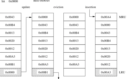
One of the most known algorithms in cache line replacement is the LRU [16]. This algorithm tries to exploit temporal locality in recently accessed lines. For this, LRU keeps the lines that has been accessed most recently since it supposedly will be ac-cessed in the near future.
LRU works like a stack. For each set, the least recently used (LRU) line is at the bottom of the stack, while the most recently used (MRU) line is at the top. Whether we have a miss or a hit, the referenced line will be inserted at the MRU position. When there is a replacement the line at the LRU position of the stack will be evicted. This algorithm is described in Figure 4.
miss or hit {
Put line at the MRU position }
replacement {
Evict line at the LRU position }
Figure 4: LRU algorithm
In Figure 5 we can see a brief sequence of accesses. Each cache set is divided in 8 slots, each one representing a line of the cache. Each line is identified by its tag. The striped cache line represents the replacement candidate, in this case the line in the LRU position.
When there is a hit (0x0000), the referenced line goes to the MRU position and the other lines move forward in the stack. In the miss (0x00A4) the LRU line (0x00B1) leaves the cache and the new line is inserted in the MRU position. The other lines
0000000 0000000 0000000 0000000 0000000 0000000 1111111 1111111 1111111 1111111 1111111 1111111 000000 000000 000000 000000 000000 000000 111111 111111 111111 111111 111111 111111 000000 000000 000000 000000 000000 000000 111111 111111 111111 111111 111111 111111 0x00B1 0x00A3 0x0012 0x0020 0x0013 0x00B4 0x0043
update eviction insertion hit 0x0000 0x00A3 0x0012 0x0020 0x00B4 0x0043 0x0000 0x0013 0x0043 0x00B4 0x0013 0x0020 0x0012 0x00A3 0x0000 0x00A3 0x0013 0x00B4 0x0043 0x0000 0x00A4 0x0012 0x0020 LRU MRU 0x0000 0x00B1
Figure 5: LRU example. Sequence of cache accesses. The vertical groups of boxes represent a cache set, being each box a line. Each line is identified by its tag in hexadecimal. The striped lines are the eviction candidates.
LRU is not usually implemented in the Last Level Cache (LLC), since the cost of the implementation increases with the associativity [13] [14].
2.2
Non Recently Used
Another well-known replacement algorithm is the NRU [17]. The purpose of NRU is the same as LRU: to keep in cache the most recent lines in order to exploit temporal locality. However, it uses less information than LRU. Instead of tracking the exact order in which the lines are referenced, it only excludes the last referenced line against eviction. By doing this it will have less precision when evicting a line, and probably less hit rate. A specific implementation of NRU groups the lines in two categories: recently used and non recently used.
In Figure 6 we see the NRU algorithm. In a hit or a miss it will mark the referenced line as RU (Recently Used), and if all the other lines in the same set are also marked to RU, it will mark them to NRU (Non Recently Used). When there is a replacement, a random line of the NRU group is evicted.
miss or hit { Set RU line
if (all lines RU) { Set NRU all lines Set RU line }
}
replacement {
Evict random line between the NRU }
Figure 6: NRU algorithm
Figure 7 is an example of the behavior of the NRU algorithm. Each cache set is divided in 8 slots, each one representing a line of the cache. Each set now has two different line groups: the blank ones representing the RU lines and the striped ones representing the NRU lines.
If there is a hit on a NRU line (0x0000) it is updated to RU. In a miss (0x00A4) a random line of the NRU group (0x00B4) is evicted. Then the new line is inserted in the RU group.
0000000 0000000 0000000 0000000 0000000 1111111 1111111 1111111 1111111 1111111 000000 000000 000000 000000 000000 111111 111111 111111 111111 111111 000000 000000 000000 000000 000000 111111 111111 111111 111111 111111 0000000 0000000 0000000 0000000 0000000 1111111 1111111 1111111 1111111 1111111 000000 000000 000000 000000 000000 111111 111111 111111 111111 111111 000000 000000 000000 000000 000000 111111 111111 111111 111111 111111 000000 000000 000000 000000 000000 000000 111111 111111 111111 111111 111111 111111 0x00B1 0x00A3 0x0012 0x0020 0x0013 0x00B4 0x0043 0x00B1 0x00A3 0x0012 0x0020 0x0013 0x00B4 0x0043 0x00B1 0x00A3 0x0012 0x0020 0x0043 0x00B1 0x00A3 0x0012 0x0013 0x00A4 0x0043 0x0020 0x0013
update eviction insertion hit 0x0000
0x0000
0x0000 0x0000 0x0000
Figure 7: NRU example. Sequence of cache accesses. The vertical groups of boxes rep-resent a cache set, being each box a line. Each line is identified by its tag in hexadecimal. The striped lines are the eviction candidates.
A simple NRU implementation would use one bit per cache line and a pointer to select amongst the NRU lines.
2.3
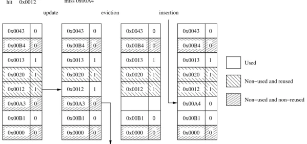
Least Recently Reused
Various algorithms have been studied in order to improve hit rates in the Last Level Cache (LLC). One of them is the LRR. This algorithm is based on the assumption that not all blocks referenced in the LLC will have reuse in the LLC, since the reuse is exploited in the lower cache levels. Therefore, LRR will predict reuse on a line referenced at least twice (the initial miss and a hit).
LRR groups the cache lines of each set in three different groups, as seen in Figure 8:
• Non-used non-reused
The most priority group is the used one, since it means that this line is currently in lower cache levels. The non-used reused group is where lines that have shown reuse but are not in any private cache are. Finally, the least priority group is the non-used non-reused group, composed by cache lines that have not been reused and are not in any private cache. Each of this groups is ordered by Recently Used, just like the LRU algorithm. 000000000 000000000 000000000 000000000 000000000 111111111 111111111 111111111 111111111 111111111 0000000000 0000000000 0000000000 1111111111 1111111111 1111111111 Used Non−used Reused Non−reused Eviction order Figure 8: LRR groups
In Figure 9 we see the LRR algorithm. When there is a miss or a hit the referenced line is moved to the MRU position of the used group. Additionally, on a hit the line is marked as reused. On a replacement the LRU line of the less priority group that exists is evicted. When a line is evicted from the last private cache, then the line leaves the used group and goes to the non-used group that matches with its reused bit.
Put line at the MRU position of the used group }
hit {
Put line at the MRU position of the used group and mark reused }
replacement {
if (non-used non-reused group not empty)
Evict line at the LRU position of the non-used non-reused group else if (non-used reused group empty)
Evict line at the LRU position of the non-used reused group else
Evict line at the LRU position }
last private cache eviction { if (reused) {
Put line at the MRU position of the non-used reused group }
else {
Put line at the MRU position of the non-used non-reused group }
}
Figure 9: LRR algorithm
In Figure 10 there is an example of how LRR works. The set is ordered by groups, and inside each group by use temporality. The reuse bit is shown next to each line tag.
In a hit (0x0012) the line is moved to the MRU position of the used group, and is marked as reused. When there is a miss (0x00A4), the LRU line of the non-used non-reused group (0x0000) is evicted. Finally, the new line is inserted in the used group with the reuse bit set to 0.
000000 000000 000000 000000 000000 111111 111111 111111 111111 111111 00000000000000 0000000 1111111 1111111 1111111 0000000 0000000 0000000 1111111 1111111 1111111 000000 000000 000000 000000 000000 000000 111111 111111 111111 111111 111111 111111 000000 000000 000000 111111 111111 111111 000000 000000 000000 000000 000000 111111 111111 111111 111111 111111 0000000 0000000 0000000 0000000 0000000 1111111 1111111 1111111 1111111 1111111 0000000 0000000 0000000 0000000 0000000 1111111 1111111 1111111 1111111 1111111 0000000 0000000 0000000 0000000 0000000 0000000 1111111 1111111 1111111 1111111 1111111 1111111 0000000 0000000 0000000 0000000 0000000 1111111 1111111 1111111 1111111 1111111 0000000 0000000 0000000 0000000 0000000 1111111 1111111 1111111 1111111 1111111 0000000 0000000 0000000 0000000 0000000 0000000 1111111 1111111 1111111 1111111 1111111 1111111 000000 000000 000000 000000 000000 111111 111111 111111 111111 111111 000000 000000 000000 111111 111111 111111 000000 000000 000000 111111 111111 111111 000000 000000 000000 000000 000000 000000 111111 111111 111111 111111 111111 111111 0000 0000 0000 1111 1111 1111 0000 0000 0000 0000 1111 1111 1111 1111
update eviction insertion hit 0x0012 miss 0x00A4
0x0043 0x00B4 0x0013 0x0020 0x0012 0x00A3 0x00B1 1 0 0 0 1 1 0 0 0x0012 0x0043 0x00B4 0x0013 0x0020 0x00A3 0x00B1 0 0 0 0 1 1 0 0x0020 0x00A3 0x00B1 0 0 0 1 1 0 0x0013 0x00B4 0x0043 0x0012 0x0012 0x0043 0x00B4 0x0013 0x0020 0x00A3 0x00B1 0x00A4 0 0 0 0 0 1 1 1 1 1 Used Non−used reused Non−used non−reused LRU MRU 0x0000 0x0000
Figure 10: LRR example. Sequence of cache accesses. The vertical groups of boxes represent a cache set, being each box a line. Each line is identified by its tag in hexadecimal. The bit next to each tag is the reuse bit.
When implementing LRR, its complexity increases with the set associativity like LRU.
2.4
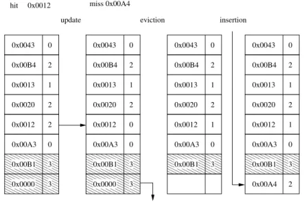
Non Recently Reused
NRR is an algorithm that simplifies the LRR implementation but keep its objectives, analogously to NRU with LRU. The idea is to keep the same groups that LRR had but without maintaining a temporal order inside the groups.
Figure 11 explains the NRR algorithm. When there is a miss or a hit the line is put in the used group. On a hit, it is also marked as RR (Recently Reused), and if the non-used non-reused group is empty, all the lines of the non-used reused group are moved to the non-used non-reused group. On a replacement the eviction order is the same as in LRR, but inside each group the line is randomly selected. When a line is evicted from the last private cache it is moved to the non-used group that matches its reuse bit.
Put line in the used group }
hit {
Put line in the used group Mark reused line
if (non-used non-reused group is empty) {
Move all non-used reused lines to non-used non-reused }
}
replacement {
if (non-used non-reused group not empty)
Evict random line from the non-used non-reused group if (non-used reused group not empty)
Evict random line from the non-used reused group else
Evict random line }
last private cache eviction { if (reused) {
Put line in the non-used reused group }
else {
Put line in the non-used non-reused group }
}
Figure 11: NRR algorithm
In Figure 12 we can see an example of a hit and a miss. The set is divided in three groups, maintaining no particular order inside each group. The reuse bit is next to the tag of each line. When there is a hit the line on the non-used reused group is moved to the used group. On a miss the replacement evicts a random line of the non-used non-reused group, and then inserts the new line in the used group without the reuse bit set.
000000 000000 000000 000000 000000 111111 111111 111111 111111 111111 0000000 0000000 0000000 0000000 0000000 1111111 1111111 1111111 1111111 1111111 000000 000000 000000 000000 000000 000000 111111 111111 111111 111111 111111 111111 000000 000000 000000 111111 111111 111111 0000000 0000000 0000000 0000000 0000000 0000000 1111111 1111111 1111111 1111111 1111111 1111111 0000000 0000000 0000000 1111111 1111111 1111111 0000000 0000000 0000000 0000000 0000000 0000000 1111111 1111111 1111111 1111111 1111111 1111111 0000000 0000000 0000000 1111111 1111111 1111111 000000 000000 000000 000000 000000 000000 111111 111111 111111 111111 111111 111111 000000 000000 000000 111111 111111 111111 000000 000000 000000 000000 000000 111111 111111 111111 111111 111111 0000000 0000000 0000000 0000000 0000000 1111111 1111111 1111111 1111111 1111111 0000000 0000000 0000000 0000000 0000000 1111111 1111111 1111111 1111111 1111111 000000 000000 000000 000000 000000 111111 111111 111111 111111 111111 000000 000000 000000 111111 111111 111111 0000000 0000000 0000000 1111111 1111111 1111111 000000 000000 000000 111111 111111 11111100000000 0000 1111 1111 1111 0000 0000 0000 0000 1111 1111 1111 1111
update eviction insertion hit 0x0012 miss 0x00A4
Used
Non−used and reused Non−used and non−reused 0x0043 0x00B4 0x0013 0x0020 0x0012 0x00A3 0x00B1 1 0 0 0 1 1 0 0 0x0043 0x00B4 0x0013 0x0020 0x0012 0x00A3 0x00B1 1 0 0 0 1 1 0 0 0x0043 0x00B4 0x0013 0x0020 0x0012 0x00B1 1 0 0 1 1 0 0 0x0043 0x00B4 0x0013 0x0020 0x0012 0x00B1 1 0 0 1 1 0 0 0 0x00A4 0x0000 0x0000 0x0000 0x0000
Figure 12: NRR example. Sequence of cache accesses. The vertical groups of boxes represent a cache set, being each box a line. Each line is identified by its tag in hexadecimal. The bit next to each tag is the reuse bit.
A simple NRR implementation will only need an extra reuse bit per cache line to track the reuse and a pointer, since it uses the presence vector to know which lines are in use.
2.5
Static Re-Reference Interval Prediction
Static Re-Reference Interval Prediction (SRRIP) [7] is based on the same idea as NRR and LRR: to keep reused lines in the cache more time than non-reused lines. However, its behavior is different from NRR and LRR. SRRIP gives each cache line a value called Re-Reference Interval Prediction (RRIP). Lines with a high RRIP value will be evicted before lines with lower RRIP value.
In Figure 13 we see the SRRIP algorithm. Each cache line has M bits to represent the RRIP value. The highest RRIP value (2M-1) lines are the eviction candidates. When a line misses, it gets a (2M-2) RRIP value and when it hits, it gets a 0 RRIP
value. In a replacement, if there are no more RRIP value of 2M-1, all RRIP values
Put line and set RRIP to (2^M)-2 } hit { Set RRIP to 0 } replacement {
while (not exists one line with RRIP (2^M)-1) { Increment all RRIP by 1
}
Evict random line with RRIP (2^M)-1 }
Figure 13: SRRIP algorithm
In Figure 14 we can see an example of a hit and a miss. Each line has a RRIP value between 0 and 3 (M = 2).
When there is a hit (0x0012) the line updates its RRIP value to 0. On a miss (0x004A) the replacement evicts a random line between the lines with RRIP value 3 (2M-1) and
then inserts the new line with a RRIP value of 2 (2M-2).
000000 000000 000000 000000 000000 111111 111111 111111 111111 111111 000000 000000 000000 000000 000000 000000 111111 111111 111111 111111 111111 111111 0000000 0000000 0000000 0000000 0000000 1111111 1111111 1111111 1111111 1111111 0000000 0000000 0000000 0000000 0000000 1111111 1111111 1111111 1111111 1111111 0000000 0000000 0000000 0000000 0000000 0000000 1111111 1111111 1111111 1111111 1111111 1111111 000000 000000 000000 000000 000000 111111 111111 111111 111111 111111 0x00B1 3 0x00B1 3 update eviction insertion
hit 0x0012 miss 0x00A4
1 3 3 0 2 2 2 0 0 0 1 0 1 0 0x0043 0x00B4 0x0013 0x0020 0x0012 0x00A3 0x0043 0x00B4 0x0013 0x0020 0x0012 0x00A3 0x0043 0x00B4 0x0013 0x0020 0x0012 0x00A3 0x00B1 3 3 0 2 2 1 1 2 2 0 1 2 2 0 2 0x00A4 0x0043 0x00B4 0x0013 0x0020 0x0012 0x00A3 0x00B1 0x0000 0x0000
Figure 14: SRRIP example. Sequence of cache accesses. The vertical groups of boxes represent a cache set, being each box a line. Each line is identified by its tag in hexadecimal. The number next to it represents the RRIP value. The stripped lines are the eviction candidates.
2.6
Set Dueling
A problem with replacement algorithms in a chip multiprocessor is that committing to a single replacement algorithm can be harmful for some of the programs. A solu-tion to this problem is to use a dynamic insersolu-tion policy, which selects between two different algorithms using Set Dueling [15].
A straightforward implementation of Set Dueling would be to use an extra tag di-rectory for each cache line, keeping track of both algorithms and using the one that misses the least. However, this is an expensive implementation and it is not used. A cost-efficient way of implementing set dueling is via set samples. As seen in Figure 15 some sets implement one algorithm (1, 4) while others (2, 7) implement a different one. These sets are the sample sets, and using a saturated counter we increase it when one algorithm misses on its sample sets and decrease it when the other misses on its sample sets. A sampling time is defined, and when that time passes, the counter is reset to 0 and the winning algorithm is used in the rest of sets (0, 3, 5, 6) until the next sampling time is up.
0000 0000 0000 1111 1111 1111
0000
0000
1111
1111
0000 0000 0000 0000 1111 1111 1111 11110000
0000
0000
1111
1111
1111
000 000 000 000 111 111 111 111000
000
111
111
Set 0 Set 1 Set 2 Set 3 Set 4 Set 5 Set 6 Set 7 Alg0 set Alg1 set + _ Alg1 miss Alg0 miss CountFigure 15: Set Dueling. Some sets are the sample sets for each algorithm. When algorithm 0 misses on its sample sets it increases the counter, while an algorithm 1 miss on its sample sets decreases it.
cache lines with a distant re-reference interval prediction (value of 2 -1) and some lines with a long re-reference interval prediction (value of 2M-2).
However, in cases where this does not happen, using BRRIP would decrease perfor-mance. Set dueling is used to select which algorithm is better for each execution. Dynamic Re-Reference Interval Prediction (DRRIP) is the algorithm that uses Set dueling to choose between SRRIP and BRRIP.
2.8
Dynamic Re-Reference Interval Prediction with
Protec-tion
In DRRIP a block present in lower level caches can be evicted if its RRIP value is 2M-1. This is not the desired behavior under the hypothesis that lines present in lower caches will be eventually reused.
Dynamic Re-Reference Interval Prediction with Protection (DRRIP+) protects the lines present in the lower cache levels when there is an eviction. When a block present in the lower cache levels is about to be evicted, its RRIP value is decremented by one and a new candidate is selected. Only when all the remaining candidate lines are present in the lower level cache one of them will be evicted.
2.9
Thread-Aware Dynamic Re-Reference Interval
Predic-tion
Since a multicore processor can have multiple programs running at the same time, there could be a program that would benefit from BRRIP and another that would harm from it. TADRRIP [4] addresses this problem. Instead of having a single policy selection counter and a group of sample sets, it has as many counters and groups of sample sets as processors. This way each program can have the algorithm that suits it best, without being influenced by other programs.
3
Simulation
Simulations will be run in order to compare the different replacement algorithms and its influence in the performance of the system. First we explain the Simulator tools used. Then we explain the simulated system and specifically the memory hierarchy.
3.1
Simulator
In order to simulate the system we need to use 3 different simulation tools, as shown in Figure 16.
3.1.1 SIMICS
SIMICS is a functional simulator that can run unchanged programs for specific ar-chitectures (for example x86-64, ARM, MIPS, SPARC...). The operating system simulated in SIMICS is Solaris.
3.1.2 GEMS: Ruby
General Execution-driven Multiprocesor Simulation (GEMS) is a suite of diverse mod-ules that implement extra functionalities to SIMICS. In this simulation we use Ruby, a memory hierarchy simulator. Ruby simulates the whole cache hierarchy, including the L1i, L1d, L2 and L3, its internal networks and the replacement algorithms. It also simulates the coherence protocol specified in the Specification Language Includ-ing Cache Coherence (SLIC) domain specific language.
3.1.3 DRAMSim2
DRAMSim2 is a module that simulates the DRAM. Amongst its functionalities it can simulate different page policies, such as open page and close page, different mapping
DRAM Caches DRAMSIM2 RUBY CPUs SIMICS
Figure 16: Simulation tools used
3.2
Simulated system
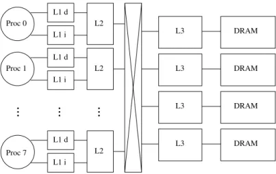
The simulated system is formed by 8 SPARC IV processors, 8 L1 caches, 8 L2 caches, a shared L3 cache divided in 4 banks and 4 memory controllers each one connected to an L3 bank. The memory lines have a size of 64B. In Figure 17 we see a schematic representation of the simulated system.
Proc 0 Proc 1 L1 d L1 i L1 d L1 i L2 L2 L2 L1 d L1 i Proc 7 DRAM DRAM DRAM DRAM
...
L3 L3 L3 L3...
...
Figure 17: Simulated system
3.2.1 Caches and DRAM specification
Private L1i / L1d 32KB, 4-way, 64B line size, LRU replacement, 1-cycle access latency
Private L2 256KB, 8-way, 64B line size, LRU replacement, 7-cycle access latency
Shared L3 8MB inclusive (4 banks of 2MB each), 64B line size. Each bank: 16-way, 10-cycle access latency DRAM 32GB divided in 4 cache controllers, 8 ranks,
64K rows, 1K columns, DDR3 1333 MHz Table 1: Cache and DRAM characteristics
In the simulations we will vary the replacement algorithm used in the L3 cache in order to analyze their behavior. The replacement algorithms user are: LRU, NRU, LRR, NRR, DRRIP and DRRIP+. The DRRIP and DRRIP+ implementations will use RRIP values of 3 bits.
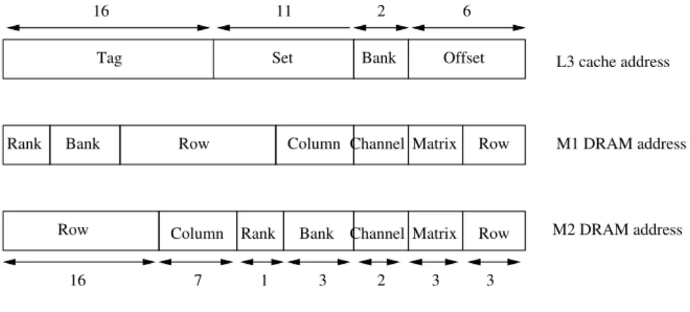
The L2 and L3 cache address mapping is seen in Figure 18.
6 2 11 Bank Set Tag 6 L2 cache address L3 cache address Set Tag 9 Offset Offset Figure 18: L3 mapping
3.2.2 DRAM mapping and page policy
We will simulate two different DRAM mappings, shown in Figure 19:
• Mapping 1
In the mapping 1, dirty line evictions from the L3 cache can or can not be mapped to the same bank and rank. The access latency will be lower if they are mapped to different bank and rank than the same.
different row, since the bits that map the set in the L3 cache are the same. This means that in a dirty line eviction the latency will always be equal or higher than mapping 1.
Bank Rank Column Bank 2 L3 cache address M1 DRAM address M2 DRAM address Tag Set 11 16 6 Row Bank
Rank Column Channel
Offset Row Matrix Matrix Row 3 2 3 3 Channel Row 1 7 16
Figure 19: DRAM mapping
Another simulation parameter will be the page policy. We will simulate a DRAM with open and close page:
• Open page
After each access it holds the row for a certain time or until it hits 4 times in the sense amplifiers. If the next access goes to the same row, it will save the time needed for a precharge-activate, but if it fails it will have to issue a precharge-activate, making the latency for this access increase. The DRAM behavior is explained in depth in the Annex B.
• Close page
Each access has to issue an activate and after the read/write a precharge.
3.3
Benchmarks
In the simulation we use 50 different benchmarks. Each benchmark has 8 applica-tions executing (one per processor). The applicaapplica-tions have been randomly selected amongst the SPEC 2000 applications. The entire benchmark list is shown in Table 2. For each benchmark we will simulate 500M cycles for filling the caches. This cycles we will not track statistics because of all the misses it would have in all the replacement algorithms. Afterwards, we simulate 1000M cycles generating statistics.
0 GemsFDTD tonto soplex soplex leslie3d xalancbmk zeusmp bwaves
1 milc milc gromacs zeusmp gromacs gromacs calculix mcf
2 gcc mcf povray leslie3d h264ref lbm namd gcc
3 libq. h264ref leslie3d sjeng zeusmp wrf omnetpp tonto
4 sphinx3 mcf povray libq. lbm leslie3d bwaves hmmer
5 libq. perlbench gobmk dealII dealII soplex leslie3d astar
6 omnetpp astar milc perlbench leslie3d libq. milc zeusmp
7 namd h264ref gobmk gromacs GemsFDTD bzip2 mcf GemsFDTD
8 h264ref bzip2 soplex sjeng perlbench gobmk zeusmp gcc
9 gamess zeusmp dealII hmmer astar GemsFDTD gcc sjeng
10 sjeng perlbench leslie3d sjeng sphinx3 wrf calculix calculix
11 sphinx3 mcf soplex bzip2 tonto sjeng mcf gamess
12 soplex h264ref bwaves gromacs soplex milc astar libq.
13 sphinx3 sjeng GemsFDTD zeusmp soplex namd dealII bzip2
14 omnetpp bwaves gobmk wrf soplex astar milc dealII
15 leslie3d gromacs leslie3d gobmk omnetpp xalancbmk gcc GemsFDTD
16 soplex namd bzip2 cactusADM gromacs leslie3d calculix leslie3d
17 zeusmp zeusmp xalancbmk leslie3d xalancbmk bwaves sjeng povray
18 libq. soplex astar calculix bzip2 GemsFDTD hmmer milc
19 libq. omnetpp zeusmp bwaves zeusmp calculix gobmk gcc
20 gobmk povray calculix cactusADM tonto GemsFDTD milc cactusADM
21 wrf mcf gobmk gromacs calculix tonto gamess bzip2
22 soplex dealII sphinx3 gobmk soplex perlbench mcf gromacs
23 milc tonto namd bwaves povray bwaves gamess hmmer
24 gcc h264ref gobmk bzip2 GemsFDTD sphinx3 h264ref omnetpp
25 sphinx3 zeusmp dealII h264ref leslie3d xalancbmk namd perlbench
26 gcc namd perlbench hmmer xalancbmk wrf xalancbmk milc
27 gamess gcc wrf perlbench gcc GemsFDTD sphinx3 povray
28 bzip2 bzip2 lbm GemsFDTD gromacs xalancbmk zeusmp bwaves
29 sphinx3 bzip2 cactusADM gamess sjeng dealII milc hmmer
30 xalancbmk tonto mcf calculix zeusmp calculix gromacs mcf
31 dealII gcc xalancbmk tonto mcf calculix gamess gamess
32 leslie3d libq. gcc sphinx3 milc bwaves dealII wrf
33 namd povray xalancbmk soplex cactusADM gamess soplex hmmer
34 calculix gamess perlbench sphinx3 GemsFDTD omnetpp omnetpp namd
35 gamess sphinx3 astar bzip2 hmmer soplex perlbench calculix
36 sjeng gobmk milc astar GemsFDTD zeusmp tonto wrf
37 leslie3d calculix gcc omnetpp sphinx3 wrf bwaves libq.
38 leslie3d mcf astar gcc gcc cactusADM bwaves leslie3d
39 hmmer soplex wrf dealII bwaves povray perlbench sjeng
40 bwaves dealII gobmk wrf zeusmp gromacs soplex leslie3d
41 xalancbmk wrf sphinx3 GemsFDTD tonto povray mcf bwaves
42 gamess tonto GemsFDTD bzip2 zeusmp gcc soplex cactusADM
43 dealII leslie3d namd gobmk tonto gcc h264ref calculix
44 tonto bwaves zeusmp wrf sphinx3 zeusmp leslie3d cactusADM
45 gromacs sphinx3 soplex namd wrf sjeng sphinx3 sjeng
46 gobmk gcc dealII soplex hmmer omnetpp cactusADM povray
4
Results
In this section the results of the simulations are presented. First, we explain the replacement algorithms performance, the eviction distribution and the energy con-sumption. Then we compare the open page and the close page policies. Finally, we analyze the mapping schemes.
4.1
Replacement algorithms
We will analyze the performance, evicts distribution per L3 bank and memory energy consumption for each replacement algorithm.
4.1.1 Performance
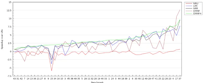
In Figure 20 we can see the speedup (CPI) over LRU of the different algorithms. The benchmarks are sorted by the DRRIP+ speedup, since it is the replacement algorithm that achieves better results overall. LRR and NRR are near DRRIP+ in performance, this is because the three algorithms protect the cache lines present in lower cache levels. DRRIP performs better in some benchmarks and worse in others, meaning that sometimes it is beneficial not to protect the lines present in the L2 cache. Finally, NRU is the worse algorithm, showing almost no improvement over LRU.
Figure 20: Performance of the different replacement algorithms over LRU. The bench-marks are ordered by DRRIP+ speedup.
In Figure 21 we see that the relation between the speedup and the misses of the DRRIP. It is clearly shown that the more misses, the higher the CPI is. The other algorithms show the same relation.
Figure 21: Relation between the performance and the misses of DRRIP. The benchmarks are ordered by DRRIP+ speedup.
can notably have more misses than the others.
Figure 22: Miss distribution by L3 bank. We can see the distribution of the L3 misses between the L3 banks for each replacement algorithm in the benchmark 33.
4.1.3 Energy consumption
In Figure 23 we can see the DRAM energy reduction over LRU for each replacement algorithm in all the benchmarks. The benchmarks have been ordered by DRRIP+ energy reduction. DRRIP+ is the one that reduces more energy, together with LRR and NRR. As it happened with the performance, DRRIP has more energy reduction in some cases and less in others. This is due the fact that the less the L3 cache misses, the less accesses to the DRAM, making the memory consume less energy.
Figure 23: DRAM energy reduction over LRU. The benchmarks are ordered by DRRIP+ energy reduction.
4.2
Page policy
Both the open page (Figure 24) and close page (Figure 25) policies perform almost exactly in all the benchmarks. The benefit of open page over close page is based on the assumption that there will be page hits in the memory. However, there are less than 1% of hits in memory accesses, making it behave similar to close page. A reason for this low amount of hit percentage is that the DRAM closes the page after a certain time without a hit or after 4 hits. A possible improvement for increasing the hit percentage would be to increase the time for the page to remain open or increase the number of hits before the page closes.
Figure 24: CPI and MPKI with Open Page. We can see the CPI and the MPKI for each replacement algorithm and program of benchmark 20.
Figure 25: CPI and MPKI with Close Page. We can see the CPI and the MPKI for each replacement algorithm and program of benchmark 20.
4.3
Mapping scheme
Between the two mapping schemes used (described in Section 3.2.2 DRAM mapping and page policy) there is no notable difference in all the benchmarks (Figure 26 and
to the same bank and rank, but different lines. In mapping 1, it can map the same line but it is highly improbable.
Figure 26: CPI and MPKI with Mapping 1. We can see the CPI and the MPKI for each replacement algorithm and program of benchmark 11.
5
Project description and planning
5.1
Project description
The main goal of the project is to compare how different replacement algorithms behave in the cache. We will also analyze the behavior of memory mapping schemes and memory page policies. In order to achieve that goal, we will use simulation software. Part of the software is provided by companies (SIMICS), but we will also work with modified code by researchers (GEMS). The modified code includes the implementations of the replacement algorithms.
The project will have three parts that will be repeated several times:
• Simulation set up
All the simulation scripts have to be programmed, the simulation code has to be compiled and installed and the different algorithms have to be understood.
• Simulation run
The different simulations will be ran. In this part of the project more software will have to be modified.
• Result analysis
Once we have the simulation results, they will be interpreted and we will do the process again with different parameters.
5.1.1 Objectives
The main goal of the project is to analyze the behavior of the replacement algorithm inside a Chip Multiprocessor (CMP).
In order to achieve the goal, we will analyze:
• How the different content management policies used in the Last Level Cache (LLC) impact the performance of the overall system.
• The distribution of misses in the LLC.
5.1.2 Risks
follow-• Already modified software
The software that we will use has already been modified in order to imple-ment the different protocols. This means that the existing software has to be understood and reviewed in case there are mistakes.
• Project planning
We must also take into consideration the time that we have to make the project. The project planning in Section 5.2 explains in depth this problem.
5.1.3 Methodology
Since we want to test the behavior of a hardware component, there are two approaches to the methodology: hardware simulation and on chip testing.
• Hardware simulation
Using simulation software reproduces the behavior of a real chip. The bench-marks run slow since the system is being simulated. On the plus side it is cheaper since we only have to pay the software licenses and hardware on where it runs.
• On chip testing
It consists in producing different chips with the desired algorithms and running the benchmarks. The benchmarks executions are fast because we are executing on actual hardware, but the cost of designing and manufacturing a new chip is really high.
For logistic and economic reasons, we will simulate the hardware using software sim-ulation tools.
5.1.4 Tools
The work tools are classified in two: hardware resources and software tools.
• Hardware resources: We will use two hardware tools:
– Desktop computer: a desktop computer will be used as a client in order to launch the simulations and program.
• Software tools: The different software tools we will use are the following:
– SIMICS software [9]: a functional simulator of computer system. It will simulate a SPARC processor and run Solaris.
– GEMS memory emulation software [10]: a module that simulates the mem-ory hierarchy system and is attached to the SIMICS simulator.
– DRAMSim2 emulation software: a module that simulates the DRAM.
– SQL database: we will set up a database in order to store and consult the simulation results.
– GNUplot: this software helps to plot different statistics.
– Bash scripts: used in order to automatize the simulation execution and data processing.
5.2
Temporal planning
5.2.1 Estimated project duration
The estimated project duration is approximately 4 months: it starts on February 17th and finishes by June 27th. The effective work days once removed holidays and weekends are 82, which divides the number of total hours of the final project (450-500) meaning that the effective time invested in the project is about 5 hours per day.
5.2.2 Project tasks
The different tasks of the project are explained, as well as the dependencies between them and some other considerations.
• Control meetings
These meetings with the directors of the project and a university professor (Angel Olive) will be held once or twice a week, with a duration of about 2 hours each meeting. In these meetings the author of the project will explain his progress and current situation.
• GEP course
The GEP course is a course on project management that must be completed in the first weeks of the final project. It includes several partial deliveries covering different areas of project management. At the end of the project a final delivery containing all the other deliveries and a presentation about the project will be done.
• Simulation software installation
The functional simulation (SIMICS) and simulator (GEMS) software must be compiled and installed on the cluster that we will use for the simulation. This task includes modifying the Makefiles in order to include different paths, envi-ronmental variables and libraries amongst others.
• Database setup
In order to access all the simulation data easily it is convenient to set up a database. The setup includes creating the tables, programming the inserts and the queries.
• Simulation scripts programming
In order to run hundreds of simulation’s the process must be automatized. For programming these scripts we need to understand the cluster’s queueing system.
• DRAM module study
The DRAM module that we will add to the existing GEMS software will be studied and the different options for adding the module to the software will be evaluated.
• Replacement algorithm study
In order to test the influence in the performance of the different replacement algorithms we must understand them. This involves reading different papers and understanding the implementations of these algorithms.
• Simulation software modifications
modi-• Simulation execution, results treatment and analysis
This three tasks generate a cycle: first we run a simulation, then we parse the results, add them to the database, plot and analyze them. We will do this process several times since we will want to obtain different statistics.
• Graphic scripts programming
Various graphics will need to be generated from the multiple results in order to help analyzing the simulations. This task will consist in testing different plot organizations to conclude the optimal for the result analysis.
• Mapping schemes study
In order to test the influence in the performance of the different mapping func-tions we must understand them.
• Final document writing
The final document with all the conclusions must be written. This process will be done in parallel with the development of the project.
• Lecture preparation
Final lecture preparation. The slides of the presentation will also be done.
• Final lecture
5.2.3 Task estimated time and dependencies
In Table 3 we see the estimated time of each task and its dependencies. In Figure 28 we see the Gantt chart of the project.
ID Task Time (h) Dependencies
1 Control meetings 40
2 GEP course 80
3 Simulation software installation 20
4 Database setup 24
5 Simulation scripts programming 14
6 DRAM module study 25
7 Replacement algorithm study 25
8 Simulation software modifications 40 6, 7,1 3
9 Simulation execution * 3, 5, 8
10 Simulation results treatment 50 12
11 Result analysis 80 12
12 Graphic scripts programming 16 13 Mapping schemes study 25 14 Final document writing 90
15 Lecture preparations 20
16 Final lecture 3 14, 15
552
Table 3: Task estimated time and dependencies
* Simulation execution time is not accounted for here because is not personal work time.
5.2.4 Gantt chart
5.2.5 Action plan
In order to ensure that everything goes as planned or to discuss different solutions in case there are any problems, there will be one or two meetings every week with the project directors.
Additionally, two weeks of the project have not been assigned to any particular task in case extra time is needed.
5.2.6 Validation method
In order to ensure the correctness of the data, the resulting measures will be calculated using different methods. Additionally, on the results analysis any abnormality will be studied in order to ensure that is its real behavior and not an error.
5.3
Project budget
The resources are divided into 3 groups: human resources, software resources and hardware resources.
5.3.1 Budget justification
The results of the project will have an impact in the performance of a multiprocessor chip. Since companies that manufacture chips need to improve the performance in each generation in order to keep competing, and these companies have high revenue (order of thousands of millions), the cost of this project is affordable. Furthermore the results of these project will be applicable to all kinds of processors: from mobile phones to desktop computers or supercomputers; because all chips nowadays are multiprocessor.
5.3.2 Human resources
There are three different tasks in the project: developer, analyst and project manager. Based on the Gantt diagram used for the time schedule, we can conclude that 40 hours (project meetings) will be of project managing, 268 hours (algorithm study and paper writing) will be of analyzing and 164 hours (programming different applications) will
Resource Price (AC/h) Time (h) Subtotal (AC) Total (AC)
Developer 20 164 3.280 4.297
Analyst 25 268 6.700 8.777
Project manager 35 40 1.400 1.834
472 11.380 14.908
Table 4: Human resources costs
5.3.3 Software resources
The memory system simulator GEMS is an open source simulator from the Univer-sity of Wisconsin, and is free of cost. The SIMICS simulator is a software tool from the company Wind River, and costs 7.500AC per year, representing a cost of 2.500AC since we will use it for 4 months. The DRAMSim2 module is open source from the University of Maryland.
5.3.4 Hardware resources
There are two different hardware costs: computer depreciation and cluster rental. The computer costs 1.200AC, and its depreciation cost will be 200AC, since we will use it 4 out of the 24 amortization months.
The cluster rental price is 0,40AC [12] per hour per core, this price includes the elec-tricity cost and any necessary maintenance. The execution time is the following:
6hours
simulation∗50simulations∗6algor∗2page policies∗2mapping schemes= 7.200hours
In Table 5 the total price with tax (21%) is calculated:
Resource Price (AC/h) Time (h) Subtotal (AC) Total (AC)
Servers 0,4 7.200 2.880 3.484
Computer 200 242
3.080 3.726 Table 5: Hardware resources costs
5.3.5 Total budget
The final budget for the project is shown in Table 6.
Resource Total cost (AC) Human capital 14.908 Software resources 2.500 Hardware resources 3.726 21.134 Table 6: Total costs
5.4
Sustainability
5.4.1 Social impact
Since the results of the project will improve a multiprocessor’s chip performance, new and more powerful applications will be possible. It will also be possible to run the same applications faster, which will represent cost and power savings.
5.4.2 Environmental impact
In the simulations we will also evaluate the power consumption of each alternative. This means that instead of only comparing the performance, we will also compare the power consumption and the performance per power consumption.
A
Cache coherence protocol
A.1
High level description
A multiprocessor system can have one or more multiprocessor chips, each one with two private cache levels and a shared cache level. The L1 cache level has separate caches for data and instructions, while the L2 cache level stores both data and instructions. The shared cache L3 is divided in banks, with a different controller each bank. There is an interconnection network that connects L2 caches, L3 banks and the memory directory. We can see a representation in Figure 29:
Proc 0 Proc 1 L1 d L1 i L1 d L1 i L2 L2 L2 L1 d L1 i Proc 7 DRAM DRAM DRAM DRAM
...
L3 L3 L3 L3...
...
Figure 29: Memory hierarchy description
A.1.1 Protocol
The L3 shared cache is inclusive and knows about all the copies in the L2s. This information is stored using one bit per cache line in a presence vector.
The L2 caches have three stable states:
• M: the cache line has been modified and its value is not updated in the L3 cache.
• S: the cache line has not been modified, it can be present in more than one L2 cache.
• M: the cache line has been modified and the memory value is not updated.
• O: the cache line is owned by this L3, and it is responsible for serving it to other L3 caches.
• S: the cache line has not been modified.
• I: the cache line is invalid, needs to fetch it from memory.
• SS: the cache line has copies in at least one of the private L2 caches.
• SO: the cache line has copies in at least one of the private L2 caches and it has been modified, the memory value is not updated.
• MT: a L2 cache has the block in exclusivity and the L3 copy is not updated.
A.1.2 Events
• L2 miss: GETS
The cache L3 controller immediatly replies to the request if it is on one of this states: M, S, O, SS or SO.
If the state is MT, the L3 cache controller requests the L2 cache that has the block that releases the exclusivity. The L2 cache line changes to the S state and sends a copy to the L3 cache. Finally, the L3 cache sends a copy to the L2 cache that requested for the line.
If the block is in I state, the L3 makes a request to the directory. The directory requests another chip or the memory for the data. If it asks another chip, the same chip is the one that sends the block. If not the memory fetches and sends the line.
• L2 miss: GETX
The L3 controller replies right away if the line is in M state.
If the line is in MT state, the L3 controller sends an invalidation request to the L2 that has the line exclusivity. This cache invalidates the line and sends a copy of it to the L3 cache. Finally, the L3 cache sends the copy to the L2 cache that requested it. If the line is in O, S or I state, the L3 controller makes a request to the directory. Then
have the line. After the acknowledgements the L3 sends the line and exclusivity to the L2 requestor.
A.1.3 Other considerations
• An L3 cache replies to all the L2 replacements.
• An L2 cache replies to all the invalidation petitions from L3.
• The network between chips is point to point and keeps the order of the messages.
• The network between the L3 and L2s is point to point and keeps the order of the messages.
A.2
Protocol implementation
In this section the implementation of a simple protocol is explained. First, we an-nounce the hypothesis for this implementation. Then we explain the different L2 and L3 requests and the transient states. Finally, we explain the state diagrams and transitions. However, in the protocol used in the simulations the L3 will be able to miss (there will be a memory) and there will be concurrency of L2 petitions.
A.2.1 Hypothesis
The hypothesis for this simplification of the protocol are:
• There is only one chip multiprocessor.
• There are no misses in the L3 cache. We suppose that the L3 acts as memory and directory.
• There is only one L2 cache petition at the same time.
Proc 0 Proc 1 Proc n L1 d L1 i L1 d L1 i L1 d L1 i L2 L2 L2
...
Network L3Figure 30: Memory system hierarchy
A.2.2 Requests
L2 uses a MSI protocol. Table 7 shows the different L2 requests.
L2 Request Description
GETS Line request for a data read
GET INSTR Line request for an instruction read GETX Line request for a write
UPGRADE Line exclusivity request for a write
PUTS Line eviction request for an unmodified line PUTX Line eviction request for a modified line
Table 7: L2 to L3 requests
L2 to L3 request L3 to L2 reply GETS DATA: data line GET INSTR DATA: data line GETX DATA: data line UPGRADE DATA: data line
PUTS ACK: acknowledgement PUTX ACK: acknowledgement
Table 8: L2 requests and L3 replies
In order to treat an L2 request, the directory (L3) can request:
• Invalidations to L2 caches that have copy of a line.
• An exclusive copy of the line in L2 to be sent to L3.
In the first case, the directory waits for the invalidation acknowledgements before answering the requestor. In the second, the directory wait the cache to send the line before replying the requestor.
The different directory requests to L2 are seen in Table 9 and its replies in Table 10.
Directory request Description
DG Send the cache line and change to S state INV Send the cache line and change to I state INV S Send the cache line
Table 9: Directory requests to L2
Directory to L2 request L2 to directory reply
DG DATA: data line
INV DATA: data line
INV S INV ACK: confirmation
A.2.3 States
The stable states of the L3 cache are shown in Table 11.
Stable state Description Possible L2 states S No L2 caches have a copy of the line I
SS At least one L2 cache has a copy of the line At least one S, others I MT An L2 cache has the line in exclusivity One in M, others I
Table 11: L3 stable states
In Table 12 the transient states of the L3 cache are explained:
Transient state Description
MO Waiting for an L2 cache to provide the line for a read MV Waiting for L2 caches with copy to invalidate
MIT Waiting for an L2 cache to provide the line for exclusivity Table 12: L3 transient states
A.2.4 State diagrams and transitions
S MO MT SS MV MIT GET_INSTR/DATA PUTS/Ack GETS/DATA GETX/INV GET_INSTR/DATA GET/DATA PUTS_last/Ack PUTX_last/Ack GETX/DATA UPGRADE_no_others/DATA Data_int_ack/DATA GETS/DG GET_INSTR/DG Data_int_ack/DATA Proc_in_ack GETX/INV_S UPGRADE/INV_S Data_int_ack/DATA
Figure 31: L3 states and transitions
In order to explain in detail the different transitions, we will analyse separately each L2 request.
• GETS and GET INSTR
S and SS
If the line is in the S or SS state, the line is directly sent to the L2 requestor, and the L2 that requested for the line is added to the presence vector. The following state after this request is the SS state.
MT
If the line is in the MT state it means that one L2 cache has it in exclusivity. The L3 controller asks for the line to the L2 cache that has it, and requests it to downgrade the exclusivity to the block. When it gets the response it sends the line to the requestor. When waiting for the response the line is in the MO state, and the line finishes in the SS state. Finally the L2 requestor is added to the presence vector.
S MO MT SS GET_INSTR/DATA GETS/DATA Data_int_ack/DATA GET_INSTR/DG GETS/DG GET_INSTR/DATA GET/DATA
Figure 32: GETS and GET INSTR transitions
• GETX and UPGRADE
S
If there are no L2 copies of the line the line is sent to the requestor. The line state is MT and the requestor is added to the presence vector.
SS
If the request is an UPGRADE and the only L2 that has the line is the requestor, it can upgrade directly without waiting.
If is an UPGRADE but other L2 caches also have the line, it has to send invali-dation messages to all the other L2s. It waits in the MV state until it receives all the acknowledgement answers, and then it allows the requestor to upgrade and ends in the MT state. It removes the previous L2 sharers from the presence vector.
If the request is a GETX it must invalidate all the L2 existing copies before send-ing the data. It also waits in the MV state until all the L2s have replied, and then sends the data and goes to the MT state. It removes the L2 previous sharers from the presence vector and adds the L2 requestor.
MT
The L3 requests for the data to the L2 cache that has exclusivity on the line. It waits on the MIT state until the L2 replies with the data, and then it is sent to the L3 cache and goes back to the MT state. It updates the presence vector removing
S MT SS MV MIT GETX/INV Data_int_ack/DATA Proc_in_ack GETX/INV_S UPGRADE/INV_S Data_int_ack/DATA UPGRADE_no_others/DATA GETX/DATA
Figure 33: GETX and UPGRADE transitions
• PUTS and PUTX
SS
If the L2 requestor is the only one that has the cache line, the presence vector is emptied and the line goes to the S state.
If there are more L2 sharers of the line, the L2 requestor is removed from the presence vector. MT
The evicted line is sent to the L3 cache and the L2 requestor is removed from the presence vector. Since no L2 caches have the line it goes to the S state.
S MT SS PUTS/Ack PUTS_last/Ack PUTX_last/Ack
B
DRAM behavior
In this section we explain how a Dynamic Random-Access Memory (DRAM) works. First, we introduce the DRAM internal organization, then we explain the different DRAM states. Afterwards, we talk about the temporal constraints between different accesses and finally we speak about the energy consumption of DRAM.
B.1
Memory system
As we can see in Figure 35, each DRAM is composed of a Memory controller and a number of Dual In-line Memory Module (DIMM)s, which are the physical boards attached to the system. Each of these DIMMs has a number of chips, and both sides of the DIMM can have chips.
Memory controller
DIMM1
DIMM0
Figure 35: DRAM DIMMs. Two DIMMs connected to the Memory controller via two logical buses.
The memory controller is connected to the DIMMs via two buses, one for com-mands and the other for data. The command bus is unidirectional while the data bus is bidirectional. All devices are connected to the same clock, which is exclusive for
serve a memory access (usually 8 chips). Inside each chip of the rank the accessed position is the same. A DIMM can have one rank per side of the memory module or just a rank in one side.
In each chip there are storage groups called banks, as seen in Figure 36. The access to each bank is independent and a group of banks can be accessed at the same time. However since they share the same I/O interface the concurrency is limited.
Banks
DIMM0
MUX I/O
Figure 36: DRAM banks. Eight DRAM banks inside a chip share the same I/O interface. In an access, each chip supplies a number of bits each cycle (usually 64 bits), and this number sets the total of bytes read per access. This number of bits are usually sent in a burst during consecutive clock cycles. In order to decrease the time of the burst, in both the rising and falling edge of the memory clock a transfer is made.
In order to supply a number of bits in parallel, each bank is divided in arrays as shown in Figure 37. Each array accesses the same line and row at the same time, supplying one bit each array.
...
...
Memory array Row decoder...
Column decoder Sense amplifiers MUX I/OFigure 37: DRAM arrays. Each bank is divided in eight arrays, in order to access them concurrently.
In a read a row is selected using the row decoder, and it is sent to the sense am-plifiers. Then the column decoder selects the desired bit. In a write the process is the same but with the difference that it does not go through the sense amplifiers.
In Figure 38 we see a memory cell. Each cell stores a bit in a transistor that acts as a capacitor. When a cell is accessed by the word line, the bit is sent through the bit line.
Word line
Capacitor Transistor
Figure 38: DRAM cell. Each bit is stored in a transistor that works as a capacitor and addressed through the bit and word line.
B.2
DRAM states
The commands used to access the DRAM are explained in Table 13.
Command Description
ACTIVATE Send a row from the array to the sense amplifiers READ Read from the line at the sense amplifiers
WRITE Write to the memory
PRECHARGE Get the open line back to the DRAM REFRESH Refresh the DRAM
Table 13: DRAM commands
In Table 14 we see a simplification of the different states and their description.
State Description Idle Ready to activate
RowActivate A row in the sense amplifiers
Precharging Waiting for the PRECHARGE to finish Refreshing Refreshing a row
PowerDown Memory not active Table 14: DRAM states
Figure 39 shows the state diagram for the DRAM. When in the Idle state the DRAM receives an ACTIVATE, it goes to the RowActivate state, and it remains there while there are READs and WRITEs. From RowActivate it goes to Precharg-ing when it receives a PRECHARGE command. It remains in the PrechargPrecharg-ing state a specific amount of time, and then goes back to Idle. When in the Precharging state, no commands are processed.
Each certain time, all the banks of a chip make a REFRESH, that is recover the electric charge they hold. Then they wait in the Refreshing state until it finishes and go back to Idle. In order to initiate a REFRESH all DRAM banks of a chip must be in the idle state.
A DRAM can go into low power under certain circumstances. We suppose that it can happen when all the banks of a chip are in Idle, then with a memory controller signal they go to the PowerDown state until the controller wakes them up again.
Idle Pre Charge Power Down Row Activate Refresh controller signal controller signal REFRESH WRITE READ PRECHARGE ACTIVATE
Figure 39: DRAM states and transitions
different ranks. In Table 15 we see a list of the abbreviations used.
Abbreviation Meaning
RL Read Latency
BL Burst Length
WL Write Latency
tRCD Row to Column Delay tRAS Row Access Strobe tRP Row Precharge
tRC Row Cycle: tRAS + tRP tWR Write Recovery
tCCD Column to Column Delay tRTP Read to Precharge
tWTR Write to Read
tRRD Row activation to Row activation Delay tRTRS Rank to Rank Switch
Table 15: DRAM latencies. Times indicated with a preceding t (tRAS, tRCD...) are expressed in DRAM cycles.
• Same bank
Before a READ or WRITE command, the row must ACTIVATE. tRCD is the time that has to pass between these commands. In order to open another row from the same bank, first there must be a PRECHARGE and then an ACTIVATE. The time between ACTIVATEs is tRC.
The burst length of the data is BL and since each cycle there are two transmissions, for the whole transfer we must wait BL/2.
ACT READ WRITE PRE READ tRCD max(tCCD,BL/2) WL+BL/2+tWTR
WRITE tRCD RL+BL/2-WL max(tCCD,BL/2)
PRE tRAS tRTP WL+BL/2+tWR
ACT tRC tRP
Table 16: DRAM same bank accesses delays. The columns are the previous commands and the rows are the following commands. Times indicated with a preceding t (tRAS, tRCD...) are expressed in DRAM cycles.
• Different bank same rank
When the consecutive accesses are to different banks, the ACTIVATE command can be sent to one bank while accessing the other one, thus increasing productivity.
ACT READ WRITE
READ max(tCCD,BL/2) WL+BL/2-RL WRITE RL+BL/2-WL max(tCCD, BL/2) ACT tRRD
Table 17: DRAM different bank same rank accesses delays. The columns are the previous commands and the rows are the following commands. Times indicated with a preceding t (tRAS, tRCD...) are expressed in DRAM cycles.
• Different rank
If the consecutive accesses are to different ranks, the delays are the same as in the same rank and different bank, since they are also different banks, but adding the delay to switch to the other rank: tRTRS. There is also no delay between ACTIVATEs because they can be issued in parallel to both ranks.
READ WRITE
READ max(tCCD,BL/2)+tRTRS WL+BL/2-RL+tRTRS WRITE RL+BL/2-WL+tRTRS max(tCCD, BL/2)+tRTRS
B.4
Energy consumption
The energy and power are computed with the ACTIVATE-PRECHARGE pair, the READ, WRITE and REFRESH commands.
B.4.1 ACTIVATE-PRECHARGE
During the ACTIVATE time there is a current consumption and thus power consump-tion as seen in Figure 40. When the line is closing in the PRECHARGE there is also energy consumption. The energy consumption during the ACTIVATE-PRECHARGE period will be called EACT.
Current IDD0 IDD2N, IDD3N Time tRAS tRP tRC PRE ACT
Figure 40: ACTIVATE-PRECHARGE current through time
The average current consumption between an ACTIVATE and a PRECHARGE will be called IDD0. There is also background energy consumption. The average
current consumption during the tRAS period is called IDD3N, and the one during the
tRP period IDD2N.
Thus, the average current coming only from the ACTIVATE and PRECHARGE commands is:
IACT =
IDD0∗tRC−IDD3N ∗tRAS−IDD2N ∗(tRC −tRAS)
tRC
And the average power, being ACTPREnumthe number of ACTIVATE-PRECHARGE
commands:
PACT =
EACT ∗ACT P REnum
T ime
B.4.2 READ and WRITE
In a READ command, the current in the BL/2 period is called IDD4R. The average
current of a READ, subtracting the background energy is:
IREAD=IDD4R−IDD3N
The energy consumption is:
EREAD =IREAD∗V ∗BL/2∗tCK
And the average power, being READnum the number of READ commands:
PREAD=
EREAD∗READnum
T ime
The WRITE command is the same as the READ, except the use of IDD4W instead
of IDD4R and the use of WRITEnum instead of READnum.
Current Time (BL/2)*tCK IDD4R IDD3N READ
B.4.3 REFRESH
In a REFRESH command all the banks from a chip are refreshed. During the refresh period (tRFC) the current is IDD5. In order to compute the REFRESH current we
must subtract the background current:
IREF RESH =IDD5−IDD3N
The energy consumption is:
EREF RESH =IREF RESH∗V ∗tRF C
And the power, being REFRESHnum the nuber of REFRESH commands:
PREF RESH =
EREF RESH∗REF RESHnum