warwick.ac.uk/lib-publications
Original citation:Guo, Zhiyong, Tian, Yanling, Liu, Xianping, Wang, Fujun, Zhang, Hongjie and Zhang, Dawei. (2016) Probe system design for three dimensional micro/nano scratching machine. Microsystem Technologies.
Permanent WRAP URL:
http://wrap.warwick.ac.uk/81324
Copyright and reuse:
The Warwick Research Archive Portal (WRAP) makes this work by researchers of the University of Warwick available open access under the following conditions. Copyright © and all moral rights to the version of the paper presented here belong to the individual author(s) and/or other copyright owners. To the extent reasonable and practicable the material made available in WRAP has been checked for eligibility before being made available.
Copies of full items can be used for personal research or study, educational, or not-for profit purposes without prior permission or charge. Provided that the authors, title and full bibliographic details are credited, a hyperlink and/or URL is given for the original metadata page and the content is not changed in any way.
Publisher’s statement:
“The final publication is available at Springer via http://dx.doi.org/10.1007/s00542-016-3115-9 "
A note on versions:
The version presented here may differ from the published version or, version of record, if you wish to cite this item you are advised to consult the publisher’s version. Please see the ‘permanent WRAP url’ above for details on accessing the published version and note that access may require a subscription.
Probe system design for three dimensional micro/nano scratching
machine
Zhiyong Guo, Yanling Tian, Jia Tian, Xianping Liu, Fujun Wang, Hongjie Zhang, Dawei Zhang Abstract
This paper presents the design and testing methodologies for a probe system used in a tip-based three dimensional micro/nano scratching machine. The probe system is one of the most important components of the
scratching machine, including an electromagnetic device and a probe suspension mechanism. The electromagnetic device is used to generate electromagnetic force to drive the probe suspension mechanism, and further scratch the
sample. The probe suspension mechanism is utilized to support the diamond probe and form the capacitor plates with the aluminum film. Both analytical modeling and finite element analysis (FEA) are conducted to improve the static and dynamic characteristics of the proposed scratching machine. A prototype has been developed to validate
the established design methodologies. A number of experimental tests have been conducted to examine the prototype performance. From the experimental results, it is noted that the developed probe system has a force
resolution of 78.4μN, a displacement resolution of 60nm, and the first natural frequency of 465Hz.This indicates that it can be used for the development of the three dimensional submicron or even nano scratching.
Keywords: probe system, micro/nano scratching, probe suspension mechanism.
1. Introduction
With the development of the micro/nano technology, the research on the application of micro/nano scale
channel in fluid mechanics or heat transfer has been receiving more and more attention. There have been many different methods for channel fabrication, including the bulk nanomachining and wafer bonding, surface
nanomachining, and buried channel technology, however, the complexity and the high cost limit the development of such kinds of techniques [1]. Lithography is another effective method, such as electron-beam lithography [2], focused ion beam lithography [3] and X-ray lithography [4], but all of these lithography methods are complemented
on wafer substrates with a complex machining procedure. The direct scratching method provides a good choice for micro/nano fabrication. Recent research efforts have been directed towards these kinds of techniques, which can be
divided into contact and non-contact scratching.
Laser scratching is a representative of the non-contact scratching, but as everyone knows the laser machining property is affected seriously by the applied laser wavelength. Longer wavelength usually changes the surface property of the sample [5, 6], and even forms the recast [7], resulting in poor precision. Shorter wavelength can
improve the scratching property, but the cost will be high.
Atomic force microscope (AFM) tip based scratching is the most popular contact scratching method, and the effect of the relevant machining parameters such as the applied load, scribing cycles, scribing speed and scribing
feed, etc, on the surface roughness and surface depth has been investigated in recent years [8-14]. However, in the
____________________________________________________________________________________________________________ Z. Guo, Y. Tian (
✉
), J. Tian, F. Wang, D. ZhangKey Laboratory of Mechanism Theory and Equipment Design of Ministry of Education, Tianjin University, Tianjin 300072, China. e-mail address: [email protected]
X. Liu
School of Engineering, University of Warwick, Coventry CV4 7AL, UK
H. Zhang
AFM tip based scratching, the machining depth is decided by controlling the contact force. This brings a problem
that the relationship between the normal force and scratching depth is usually different for different material, which makes it difficult in predicting the machining depth [15]. According to the construction of the AFM, the axis of the cantilever used to support the probe is along a single direction, resulting in that the depth is affected by the
machining direction, which has been introduced in reference [16]. Moreover, the stiffness of the probe cantilever is usually low, which makes it sensitive to the environment, especially the ambient temperature change and the
external vibration may lead to a micro thermal deformation and attendant vibration of the cantilever, and thus improve the inaccuracies of the fabricated structure.
In order to address the aforementioned issues of the AFM, many different mechanical designs have been
proposed for the probe system. W. P. Jeong [17] presented a portable nano probe system, where the sharp stylus was mounted on the probe shaft directly, which moved upwards or downwards with an air lubricated hydrostatic sliding mechanism. With this mechanism the friction between the shaft and the housing was reduced greatly, but it cannot
be totally eliminated. B. A. Gozen [18] constructed a nano milling system to fabricate the micro channel. The micro/nano structure was machined through milling and the contact detection was realized through the resonance
phenomenon of a cantilever, the disadvantage of the system is that it is difficult to fabricate a nanometer structure under 100nm due to the elliptical movement of probe.
A probe system used in a tip-based three dimensional micro/nano scratching machine is presented in this paper,
which mainly includes an electromagnetic device, a cross-shaped probe suspension mechanism and a magnetron sputtering aluminum film. In order to avoid complex calibrations between the normal force and the scratching depth for different materials, the designed scratching system adopts the displacement based method. During the
scratching, a feedback controller is organized in the proposed probe system to keep the position of the probe, and a 3-DOF high precision positioning stage dominates the scratching structure. Due to the resolution of the
electromagnetic force is theoretically infinite small, it is possible to reduce the suspension vibration in nano scale. Furthermore,the cross-shape decreases the stiffness difference of the suspension mechanism in xy plane, which can avoid the effect of the scratching direction to the scratching depth in a large extent. In the following, the design of
the three dimensional micro/nano scratching machine, especially the probe system is firstly introduced in section 2, including the theoretical modeling and finite element analysis (FEA). The whole operating procedure is then described in section 3. In the last section, the experimental setup is presented and some experiments have been
conducted to examine the prototype performance.
2. The mechanical design of the probe system
The assembly diagram of the three dimensional micro/nano scratching machine is shown in Fig. 1, which
applies the gantry structure. Two manual coarse positioning platforms are fixed orthogonally on the pedestal, and another one is assembled on the standing plate, these three platforms can be used to adjust the sample in a range of 50mm×50mm×50mm along the x/y/z axis. The vertical plate of an L-shape bracket is fixed on vertical manual
coarse positioning platform, and the horizontal plate is utilized to connect the probe system. An x/y/z 3-DOF high precision positioning stage is assembled on the two horizontally arranged manual coarse positioning platforms,
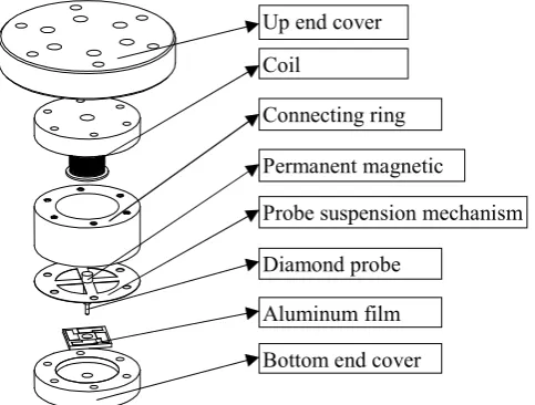
Among all of these components, the probe system shown in Fig. 2 is the most important part of the micro/nano
scratching machine, which includes the up end cover, the coil, connecting ring, permanent magnet, probe suspension mechanism, diamond probe, aluminum film, and bottom end cover. The up end cover connects the probe system on the L-shape bracket. The coil and permanent magnet form the electromagnetic device to provide
the electromagnetic force. The probe suspension mechanism organizes the capacitor plates with the aluminum film as well as support the diamond probe. The bottom end cover is used to hold the ceramic base of the aluminum film.
All these components are screwed on the connecting ring. During the scratching, the electromagnetic device and the capacitive sensor are used to organize a feedback controller to keep the probe position, and due to the
theoretically infinite small resolution of the electromagnetic force, the vibration of the probe suspension mechanism in a certain position can be suppressed effectively, and cooperate with the x/y/z 3-DOF high precision positioning stage, three dimensional micro/nano structure can be machined.
2.1. The electromagnetic device
In the probe system, the electromagnetic force drives the diamond probe directly, in order to improve the
[image:4.595.77.455.259.437.2]control precision, it is necessary to analyze the impact factor of the electromagnetic force. The schematic of the Fig. 1. The assembly diagram of the three dimensional micro/nano scratching machine.
Support frame
Manual coarse positioning
platform Probe system
x/y/z 3-DOF
precision positioning stage Sample table L-shape bracket
x y
z
Up end cover
Bottom end cover Coil
Connecting ring
Permanent magnetic
Diamond probe
Aluminum film
Probe suspension mechanism
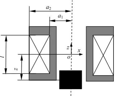
[image:4.595.198.440.486.669.2]electromagnetic device is shown in Fig. 3, where a1 and a2 are the inside and outside radius of the coil, respectively, l
is the length of coil, z is the distance from the center of the permanent magnet to the central point O of the coil. Some more electromagnetic parameters are defined, Brem and V are the residual magnetism and volume of permanent
magnet, respectively, χ is the packing factor of the coil, n is the coil turns, i is the current inputted into the coil.
The dimensions of the coil have a significant impact on the electromagnetic force, so another two parameters α and β are introduced to describe the geometry of the coil (α=a2/a1, β=l/2a1). According to the reference [19], the
electromagnetic force F along the coil axis can be calculated.
z
dH z
F B V
rem dz
(1)
The magnetic field along the axis of the coil can be calculated by following equation.
1 1 1 , / , / 0 2 , z zf z a f z a
z H H a f (2)
where
2 2
2
, ln
1 1
f
, and
1 , 0 2 1 z nif H a .Considering the difference of the independent variable in Eq. (1) and Eq. (2), the electromagnetic force computed by Eq. (1) can be transformed into
1 1 1 / / zrem dH z a
B V F
a d z a
(3)
According to Eq. (3) and the analysis of the reference [20], when the permanent magnet is positioned near the
end of the coil, the electromagnetic force reaches the maximum and the impact drawn from the distance z is minimum, so in order to obtain the maximal and the best linear force, the position of the permanent magnet should
be considered seriously and try to locate it near the coil end during the assemble of the probe system. Due to only micrometer or even nanometer scale depth in the micro/nano scratching, the electromagnetic force can be approximately seen as linear and be calculated by F=ki-F ×i, where ki-F is a constant value and decided by the above
mentioned parameters.
2.2. The probe suspension mechanism
[image:5.595.205.392.152.307.2]l a1 a2 z x z o
The probe suspension mechanism plays an important role in the probe system in terms of supporting the
diamond probe and forming the capacitor plates with the aluminum film. Because the probe suspension mechanism needs generate different deformation in the machining process, the Be/Cu alloy is selected as the material for its high elasticity. In order to improve the property of the probe suspension mechanism, the stiffness model and FEA
are implemented.
As shown in Fig. 4(a), the working part of the probe suspension mechanism is the cross beam, which has been marked 1~4. Considering the cross beam is fixed by the outside circle, it is obvious that the beam is over
constrained, but the movement along the z direction is not restrained, and the constraint of movements in other directions is helpful to improve the property of probe suspension mechanism. Every flexible beam can be seen as a
leaf-spring flexure hinge, which has been widely used in micro/nano positioning stage, and the stiffness matrix is an effective method for the stiffness analysis of this kind of flexure hinge. The global coordinate of the probe suspension mechanism is shown in Fig. 4(a), and the model of a leaf-spring flexure hinge with local coordinate is
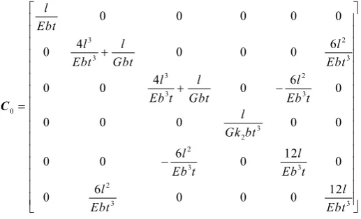
shown in Fig. 4(b). According to references [21, 22], the original compliance matrix of the leaf-spring flexure hinge in the local coordinate is
3 2 3 3 3 2 3 3 0 3 2 2 3 3 2 3 3
0 0 0 0 0
4 6
0 0 0 0
4 6
0 0 0 0
0 0 0 0 0
6 12
0 0 0 0
6 12
0 0 0 0
l Ebt
l l l
Ebt Gbt Ebt
l l l
Eb t Gbt Eb t
l Gk bt
l l
Eb t Eb t
l l Ebt Ebt C (4)
where b, l and t are the geometric dimensions of the leaf-spring hinge shown in Fig. 4(b). E and G are the Young's
modulus and the shear modulus of the material, respectively. k2 is a geometric parameter and k2 =b/t.
The local coordinate of the flexure beam 1 is defined consistent with the global coordinate, so through matrix transform, the compliance matrix of the flexure beam 1 in the global coordinate can be obtained based on the
Fx O0 t b l y0
z0 Fz
Fy Mx My Mz x0 x y z O
1 3
4 2
[image:6.595.175.434.526.683.2](b)
original leaf-spring model.
1 0-90 0 -90 0
0 -90 0 -90
T x x x x R R C C R R (5)
where R is the rotation matrix from the local coordinate to the global coordinate, and
1 0 0
( ) 0 cos sin 0 sin cos
x x x x
x x
R
.
The four beams of the probe suspension are in xy plane, so based on the compliance matrix of the flexure beam 1, the compliance matrix of other three flexure beams can be obtained through the rotation matrix transformation.
1 1 1 1 1 0 0 0 0 Tz i z i
i
z i z i
R R C C R R
i=2, 3, 4. (6)
where Rz(θi-1) is the rotation matrix from the local coordinate i to the global coordinate, and
1 1
1 1 1
cos sin 0
( ) sin cos 0
0 0 1
i i
z i i i
R
The stiffness matrix of the flexure beam is the inverse of compliance matrix, and then the stiffness matrix of
the probe suspension mechanism can be obtained as
4 -1 1 sus i i K C
(7)In order to implement the FEA, the finite element model of the probe suspension mechanism is firstly constructed in ANSYS Workbench software, the inside and outside diameters are 18mm and 30mm, respectively,
the width of the cross beam is 3mm, and the copper alloy is selected as the cross beam material. Considering the impact of the mass of permanent magnet, probe holder and diamond probe to the resonant frequency, a permanent
magnet with a diameter of 3mm and a height of 2mm and an equivalent stainless steel cylinder with a diameter 2mm and a height 9mm for the diamond probe and the probe holder are attached on the suspension mechanism.
The Young's modules, Poisson's ratio and density of the copper alloy, permanent magnet and the stainless steel are 110GPa, 0.33, 8300kg/m3, 115GPa, 0.23, 7750kg/m
3
and 193GPa, 0.31, 7750kg/m3, respectively. The meshing quality of the cross beam has a major impact on the simulation results for the thin thickness, so the cross beam is
firstly split into four separate solids with symmetric structure, and then the free meshing of every flexural beam can be very regular.
According to the stiffness analysis, the thickness of the cross beam affects the property of the probe
suspension mechanism most, so five different thicknesses with 25μm, 50μm, 75μm, 100μm, 125μm are simulated, and the simulation results are shown in Fig. 5. It indicates the stiffness of the probe suspension has an obvious rise with the increasing of cross beam thickness, and the increasing rate is about (t2/t1)3, the increasing rate of the first
natural frequency is about (t2/t1) 3/2
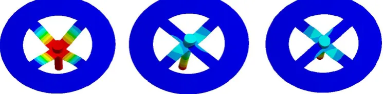
, where t2 and t1 are the thickness of the cross beam. Through the simulation, the
along the z direction, the second and third mode shapes are the rotation about the x and y direction, respectively. In
addition, the second and third natural frequencies are almost same for the symmetric structure.
Furthermore, in order to demonstrate the correctness of the stiffness modeling, the analytical and simulated stiffness of the probe suspension mechanism in the z direction with five different thicknesses are listed in table 1,
which indicates the analytical results agree well with the simulation results, but thin thickness enlarge the error, it is may be the FEA is not suitable for the micro structure simulation. But in any case, the stiffness matrix model is effective in the calculation of the stiffness of probe suspension mechanism. Based on the stiffness matrix, the
stiffness of the cross suspension mechanism and the AFM cantilever in xy plane are analyzed, the one beam of the proposed suspension can be seen as the AFM cantilever. Due to the symmetric structure, the stiffness of the both
mechanism in a range of 180º is analyzed, and the forward direction of the x axis is defined as the 0ºdirection. As shown in Fig. 7, it is obvious the stiffness of AFM cantilever has a larger change, and the stiffness in the 0º and 180º directions is about 9 times than it in the 90º direction. In contrast, the stiffness of the cross suspension is
[image:8.595.48.548.322.387.2]almost same in all directions, which means the deformation of the cross suspension has a smaller change in different scratching direction.
Table 1 The analytical and FEA stiffness of the probe suspension mechanism in the z direction
Thickness 25μm 50μm 75μm 100μm 125μm
FEA Stiffness 53.37 N/m 424.16N/m 1390.43 N/m 3296.85N/m 6284.17 N/m Analytical stiffness 48.89 N/m 391.06N/m 1319.60 N/m 3127.40N/m 6106.60 N/m
[image:8.595.196.403.408.554.2]Error 8.74% 7.80% 5.09% 5.14% 2.83%
Fig. 5. The FEA results of the probe suspension mechanism in stiffness and first natural frequency.
Fig. 6. The first three mode shapes of the probe suspension mechanism.
25 50 75 100 125
0 1000 2000 3000 4000 5000 6000 7000
Thickness (m)
S
ti
ff
n
ess (
N
/m)
25 50 75 100 125 0
100 200 300 400 500 600 700
Firs
t
n
at
u
ra
l
fr
eq
u
en
cy
(H
z)
[image:8.595.110.483.585.677.2]Fig. 7 The stiffness of the cross suspension mechanism and the AFM cantilever in xy plane
2.3. The magnetron sputtering aluminum film
In the composing of the capacitive sensor, the aluminum film is selected as another capacitor plate for the high electrical conductivity and low cost. As shown in Fig. 8, the aluminum film is divided into four parts and arranged in a cross, every part forms a capacitive sensor with the corresponding flexible beam of the probe suspension
mechanism, the area A with size 3mm×3mm acts as the capacitor plate and the area B is used for the lead bonding, the thickness of the aluminum film is 1μm. Theoretically one pair capacitor is enough for the measurement of the
deformation in the z direction, but the four flexible beams of the probe suspension mechanism are inevitable to generate different bend deformation during the scratching, multi pair capacitors enable us obtain more information about the deformation, which is helpful for the controller design.
In the selection of the aluminum film base, a polished cubic ceramic with size 10mm×10mm×1mm is a decent choice for the good electrical insulation and thermal conductivity, and in order to improve the adhesion of the aluminum film, magnetron sputtering has been a popular method. The base surface roughness affects the adhesion
between the base and the film, and considering the thickness of the aluminum film is only 1μm, the surface roughness of the ceramic base in this paper is about 0.01μm. The ceramic base needs to be cleaned in the ultrasonic cleaner before the sputtering. A magnetron sputtering deposition system (JGP-560, Chinese Academy of Sciences,
China) is used to fabricate the aluminum film.
3. The operating procedure
For the displacement based scratching method, the whole process is divided into the contact testing and the
0 30 60 90 120 150 180 0
2 4 6 8 10 12x 10
6
Angle (o)
S
ti
ff
n
e
ss
(
N/
m)
Cross suspension AFM cantilever
Fig. 8. The aluminum film arrangement on a cubic ceramic. A
B
Aluminum film
[image:9.595.183.414.565.697.2]scratching. The schematic of the three dimensional precision machining system is shown in Fig. 9. In the initial
position, there is not current in the electromagnetic device, the probe suspension generates an initial deformation to balance the self weight.
In the contact testing, the PC sends commands to the stage controller through D/A convertor 1 to drive the
3-DOF precision positioning stage rise in the z direction, simultaneously the capacitive sensor measures the gap change, and when it reaches a pre-set value Δ, the sample is deemed to contact with the probe tip, and this position of the suspension is called as reference position. Generally, a smaller contact force means a smaller indentation
during the contact test, however, for a pre-set value of gap change Δ, a higher stiffness of the suspension will lead to a bigger contact force. So for a determined contact force Fcon and the pre-set value of gap change Δ, the stiffness
of the probe suspension should be
con sus
F
K
(8)In the process of the scratching, the DC drive, D/A convertor 2 and the probe system organize a feedback
controller to keep the position of the probe suspension, When the suspension deviate the initial position, it will be driven back to the reference position by the electromagnetic force.At the same time, the PC controls the x direction and y direction movement of the 3-DOF precision positioning stage directly through the stage controller and
corresponding software, the z direction depth can still be controlled by the stage controller through the D/A convertor 1. Due to the constant position of the probe, the scratching trajectory depends on the movement of the
3-DOF precision positioning stage completely.
[image:10.595.118.491.407.559.2]4. The experimental setup
Fig. 9. Schematic of the three dimensional micro/nano scratching system. DC drive
Capacitive sensor
D/A convertor 2
A/D convertor 3-DOF precision
positioning stage
Capacitance process
circuit
Stage controller
D/A convertor 1
The experiment setup is shown in Fig. 10, three manual coarse mobile platforms (WN115TM50M, winner
optical instruments, China) arranged orthogonally are used to realize the broad adjustment, the full stroke is 50mm with a minimal regulating amount of 2μm. A home-made directive current circuit is used to drive the coil, which receives the command signals from the I/O interface of a dSPACE DS1103 R&D control board. The capacitance of
the formed capacitor is converted to voltage by a post-process circuit (E-509.C3A PI, Germany) for the further data processing. A x/y/z 3-DOF precision positioning stage (P-517.3CD, PI, Germany) with the corresponding stage
controller (E-725.3CD, PI, Germany) are used to realize the high precise movement, the colsed-loop travel is 100μm in the x and y directions and 20μm in the z direction, the closed-loop resolution is 1nm in the x and y
directions and 0.1nm in the z direction. In order to facilitate the contact testing and improve the band width of the system, the probe suspension mechanism with thickness of 100μm is selected for the experimental tests.
4.1. The measurement of input current
The current input into the coil of electromagnetic device is supplied by a direct current circuit, which is
home-made and the simplified circuit is shown in Fig. 11. The input signal Vi from the dSPACE control board is
amplified in the circuit, and in order to measure the current in the electromagnetic coil, a precision resistor connects the coil in series, the measured voltage of this resistor Vm can be used to calculate the current. Generally, a higher
current will heat the circuit component, especially the precision resistor, leading to the reduction of the current resolution, so the input current should better less than 100mA. The current resolution of the circuit is 1mA, which
[image:11.595.117.483.247.460.2]has a significant impact on the force resolution of the electromagnetic device. Fig. 10. The experimental setup.
Capacitance post-process
circuit dSPACE
control board PC
Direct current circuit
Stage controller
x/y/z 3-DOF precision
positioning stage Loadcell
Probe system Coarse mobile
platform
Fig. 11. The simplified direct current circuit. +
- K
i
Coil
Precision
resistor Vm
[image:11.595.218.397.623.750.2]4.2. The resolution of the capacitive sensor
The cross beam of the probe suspension and the aluminum film form the capacitor plates, which is seen as a
capacitive sensor and used to perceive their gap change, then the capacitance is amplified and converted to the voltage output by a post-process circuit. The calibration process of the capacitive sensor is described as follows:
remove the loadcell from the experiment setup shown in Fig. 10 and adjust the probe tip contact with the sample table, then drive the 3-DOF precision positioning stage to move in the z direction and measure the corresponding output voltage of the capacitance process circuit simultaneously, through the point by point method, the relationship
between the displacement and the voltage can be obtained. The calibration results indicate the conversion rate from the gap displacement change to the output voltage is 60nm/mV.
It is easy to know the displacement resolution of the capacitive sensor is the product of the output voltage
[image:12.595.176.401.305.421.2]resolution of the capacitance process circuit and the conversion rate, according to the measurement, the output voltage resolution is 1mV, so the displacement resolution of the capacitive sensor is 60nm shown in Fig. 12. It is noted that a better capacitance process circuit will improve the resolution effectively.
Fig. 12. The resolution of capacitive sensor.
4.3. The calibration of the electromagnetic force
In the electromagnetic device, the twining coil are with parametersa1=2.5mm, a2=5mm, l=10mm, n=400, the
permanent magnet are with residual magnetism Brem=1.2T, diameter d=3mm and height h=2mm. A loadcell
(F329UB00A0, NOVATECH, UK) with range 0.1N and resolution 10μN is used to measure the electromagnetic
force during the force calibration, which can be seen as another flexible beam with fixed stiffness, so the loadcell is inevitable to generate some deformation during the force measurement, resulting in the deformation of the probe
suspension and further offset a portion of electromagnetic force. So before the calibration of the electromagnetic force, the axial stiffness of the probe suspension Ksus should be firstly measured. The concrete method is described
as follows, same current shown in Fig. 13(a) are inputted into the coil without and with the application of the loadcell, respectively, the current increases slowly until 15mA, from the testing results, the displacement measured by the capacitive sensor without using the loadcell is 400nm (shown in Fig. 13(b)), while in the case of the loadcell,
the measured electromagnetic force is 0.5mN (shown in Fig. 13(d)), and due to the flexible deformation of the loadcell, the capacitive sensor still measures a displacement 230nm (shown in Fig. 13(c)).
F= Ksusz1 (9)
F=Floadcell+Ksusz2 (10)
where F is the electromagnetic force, Floadcell is the measured force of the loadcell, z1 and z2 are the measured
displacement of the capacitive sensor without and with the loadcell, respectively.
According to Eqs. (9) and (10), Ksus can be easily obtained, Ksus=2941.17N/m, and then use Eqs. (9) or (10)
0 2 4 6 8 10
-100 -50 0 50 100 150
Time (s)
Di
spla
ce
ment
(nm
again, the electromagnetic force is obtained, F=1.1765mN, so the conversion rate ki-F from the input current to the
electromagnetic force is 78.4μN/mA. With the above electromagnetic parameters, the conversion rate obtained from Eq. (3) is 69μN/mA, which agrees well with the experimental result. Based on the current resolution, the force resolution of the electromagnetic device resolution is 78.4μN. It is noted that the force resolution is obtained
through the calculation, which is the product of the current resolution and the force conversion rate, thus in order to improve the force resolution, we should improve the current resolution or reduce the force conversion rate, but a
lower force conversion rate means the reduction of the maximal electromagnetic force, leading to the decrease of the machining capacity, so a direct current circuit with smaller output current resolution will be a better way to
improve the force resolution.
(a) (b)
(c) (d)
Fig. 13. (a) The measured input current; (b) the measured displacement of capacitive sensor without loadcell; (c) The
measured displacement of capacitive sensor with loadcell; (d) the measured force of loadcell.
4.4. The natural frequency of the probe system
Frequency swept method has been an effective method for the natural frequency measurement [23]. A swept
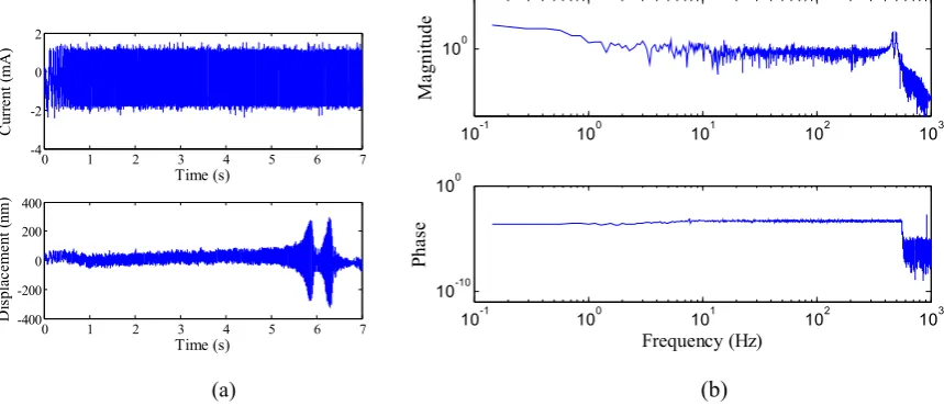
signal with small amplitude is inputted into the coil to active the resonant phenomenon of the probe system, and simultaneously makes a measurement for the generated displacement of the probe suspension mechanism. The measured time domain current signal and displacement signal are shown in Fig. 14(a), and then through data
process, the corresponding frequency domain response is displayed in Fig. 14(b). According to the measurements, the magnitude in Fig. 14(b) has two peaks with frequencies 465Hz and 498Hz, it is because the second and third
resonant frequencies of the probe suspension are with same value, which have been observed in the FEA. From the testing results of section 4.3 and 4.4, both the stiffness and the first natural frequency of the probe suspension mechanism are a little less than the simulation results, which may be caused by the thickness error of the cross
beam, or the fact that the practical elastic property of the material is a little poor.
0 1 2 3 4 5 6 7
-20 -15 -10 -5 0 5 Time (s) C ur re nt ( m A )
0 1 2 3 4 5 6 7
-600 -400 -200 0 200 Time (s) Di spl a ce me n t (nm )
0 1 2 3 4 5 6 7
-300 -250 -200 -150 -100 -50 0 50 Time (s) Dis p la ce m ent ( nm)
0 1 2 3 4 5 6 7
[image:13.595.70.506.225.513.2](a) (b)
Fig. 14. The dynamic response of the probe system: (a) time domain response, (b) frequency response.
4.5. The scratching of submicron channel
In order to validate the machining ability of the constructed experimental setup, a group of submicron channels with 6μm length and 80nm depth have been scratched on a copper cube, which is with the dimension
5×5×1mm and surface roughness 20nm. A diamond Berkovich probe was selected as the cutting tool. The channel is scratched two times in y direction and with a small feed 300nm between the two scratching. The scratched
channel and the vertical cross-section of the channle in three positions are shown in Fig. 15. The arrow a is the ridge top of the first groove, the arrow b and d are the ridge top of the second groove, the arrow c is the bottom of the second grrove. According to the Fig. 15, the channel depth is about 80nm in all three cross-sections, which
means the probe tip position is kept almost constant during the scratching. The ridges are obvious in the both sides of the grooves, this is because the sample is with strong plasticity, and another reason is the face angle (65.3°) of
the Berkovich probe is so big that the removed materials cannot flowed away timely. Moreover, the first groove was fulfilled by the left ridge of the second groove.
0 1 2 3 4 5 6 7
-4 -2 0 2
Time (s)
C
u
rr
e
nt
(
mA)
0 1 2 3 4 5 6 7
-400 -200 0 200 400
Time (s)
D
is
plac
e
m
e
nt
(
nm)
10-1 100 101 102 103
100
M
a
gnit
ude
10-1 100 101 102 103
10-10 100
Frequency (Hz)
P
ha
se
a b
c
d
Fig. 15. The scratched nanochannel.
5. Conclusions
A probe system used in a tip-based three dimensional micro/nano scratching machine is designed, which mainly includes an electromagnetic device and a probe suspension mechanism, through the respective simulation
validation, the established theoretical model can be used to guide the structure design. Some testing methodologies are introduced and the corresponding experiments are implemented on the constructed prototype, it is noted the
electromagnetic force conversion rate is 78.4μN/mA, the stiffness and the first natural frequency of the probe system are 2941.17N/m and 465Hz, respectively, which verifies the correctness of the theoretical and simulation analysis. Furthermore, the developed probe system has a displacement resolution of 60nm and a force resolution of
78.4μN, a nanochannel with 6μm length and 80nm depth has been scratched on a copper sample, indicating it can be used for the development of the three dimensional submicron scratching or even nano scratching.
ACKNOWLEDGEMENTS
This research is supported by National Natural Science Foundation of China (Nos. 51275337, 51175372,
51205279, 51405333, 51420105007), National Key Special Project of Science and Technology of China (No. 2011ZX04016-011), Reserved Academic Program of Peiyang Scholar, and Program for New Century Excellent
Talents in University (No. NCET-11-0374).
REFERENCES
Perry JL, Satish SG (2006) Review of fabrication of nanochannels for single phase liquid flow. Microfluidics and Nanofluidics 2(3): 185–193
a b
c d
(c)
a b
c d
Kang MS, Lee JH, Bahng W et al (2014) Top-down fabrication of 4H-SiC nano-channel field effect transistors. Journal of nanoscience and nanotechnology 14(10): 7821-7823
Erdmanis M, Sievila P, Shah A et al (2014) Focused ion beam lithography for fabrication of suspended nanostructures on
highly corrugated surfaces. Nanotechnology 25(33): 33502
Giorgis V, Zilio P, Massari M et al (2014) Fabrication of multiple large arrays of split ring resonators by X-ray
lithographic process for sensing purposes. Microelectronic engineering 127: 68-71
Yang C, Mei X and Wang W (2014) Comparative experimental study of laser-induced transitions in crystalline silicon by femtosecond, picosecond, and millisecond laser ablation. Radiation Effects & Defects in Solids 169(3): 194–203
Reimers H, Gold J et al (2003) Topographical and surface chemical characterization of nanosecond pulsed-laser micromachining of titanium at 532-nm wavelength. Applied Physics A – Materials Science & Processing 77(3):
491–498
Yang C, Mei X and Wang W (2013) Recast layer removal using ultrafast laser in titanium alloy. International Journal of Advance Manufacturing Technology 68(9): 2321–2327
Fang TH, Weng CI, Chang JG (2000) Machining characterization of the nano-lithography process using atomic force microscopy. Nanotechnology 11(3): 181–187
Fang TH, Chang WJ (2003) effects of AFM-based nanomachining process on aluminum surface. Journal of Physics and Chemistry of Solids 64(6): 913–918
Yan Y, Sun T et al (2007) Investigation on AFM-based micro/nano-CNC machining system. International Journal of
Machine Tools & Manufacture 47: 1651–1659
Mao YT, Kuo KC et al (2009) Research on three dimensional machining effects using atomic force microscope. Review
of scientific instruments 80: 065105
Geng Y, Yan Y, Zhao X (2013) Fabrication of millimeter scale nanochannels using the AFM tip-based nanomachining method. Applied Surface Science 266: 386-394
Zhang P, Zhao H et al (2013) Influence of double-tip scratch and single-tip scratch on nano-scratching process via molecular dynamics simulation. Applied Surface Science 280: 751–756
Bourne K, Kapoor SG, DeVor RE (2010) Study of a high performance AFM probe-based microscribing process. Journal of Manufacturing Science and Engineering 132(3): 030906
Geng Y, Yan Y, Xing Y (2013) Modelling and experimental study of machined depth in AFM-based milling of
nanochannels. International Journal of Machine Tools & Manufacture 73: 87–96
Yan Y, Sun T et al (2009) Effects of scratching directions on AFM-based abrasive abrasion process. Tribology
International 42(1): 66–70
Jeong WP, Soo CC, Hyun C (2011) Portable nano probe for micro/nano mechanical scratching and measuring. Trans. Nonferrous Met. Soc. China 21(1): S205−S209
Gozen B A, Ozdoganlar OB (2012) Design and evaluation of a mechanical nanomanufacturing system for nanomilling. Precision Engineering 36(1): 19-30
Smith ST, Chetwynd DG (1990) An optimized magnet-coil force actuator and its application to precision elastic mechanisms. Proceedings of the Institution of Mechanical Engineers, Part C: Journal of Mechanical Engineering Science 204(4): 204-243
Robertson W, Cazzolato B and Zander A (2012) Axial force between a thick coil and a cylindrical permanent magnet: optimizing the geometry of an electromagnetic actuator. IEEE Transactions on magnetics 48(9): 2479-2487
Lai L, Gu G, Zhu L (2012) Design and control of a decoupled two degree of freedom translational parallel micro-positioning stage. Review of Scientific Instruments 83(4): 045105
Kim H, Gweon DG (2012) Development of a compact and long range XY theta(z) nano-positioning stage. Review of