http://wrap.warwick.ac.uk/
Original citation:
Lazenby, Robert A., McKelvey, Kim M. (Kim Martin), Peruffo, Massimo, Baghdadi, Marc
and Unwin, Patrick R.. (2013) Nanoscale intermittent contact-scanning electrochemical
microscopy. Journal of Solid State Electrochemistry . ISSN 1432-8488 (In Press)
Permanent WRAP url:
http://wrap.warwick.ac.uk/57250
Copyright and reuse:
The Warwick Research Archive Portal (WRAP) makes this work of researchers of the
University of Warwick available open access under the following conditions. Copyright ©
and all moral rights to the version of the paper presented here belong to the individual
author(s) and/or other copyright owners. To the extent reasonable and practicable the
material made available in WRAP has been checked for eligibility before being made
available.
Copies of full items can be used for personal research or study, educational, or
not-for-profit purposes without prior permission or charge. Provided that the authors, title and
full bibliographic details are credited, a hyperlink and/or URL is given for the original
metadata page and the content is not changed in any way.
Publisher’s statement:
The final publication is available at link.springer.com
http://dx.doi.org/10.1007/s10008-013-2168-2
A note on versions:
The version presented here may differ from the published version or, version of record, if
you wish to cite this item you are advised to consult the publisher’s version. Please see
the ‘permanent WRAP url’ above for details on accessing the published version and note
that access may require a subscription.
1
Nanoscale Intermittent Contact-Scanning
Electrochemical Microscopy
Robert A. Lazenby,1 Kim McKelvey,1,2 Massimo Peruffo,1 Marc Baghdadi1,2 and Patrick R. Unwin*,1
1 Department of Chemistry, University of Warwick, Coventry, U.K., CV4 7AL.
2 Molecular Organization and Assembly in Cells (MOAC) Doctoral Training Centre (DTC), University of Warwick,
Coventry, U.K. CV4 7AL.
*Corresponding author: e-mail [email protected], telephone +44 (0) 2476 523264, fax : +44 (0) 2476 524112.
Submitted to J. Solid State Electrochem., Bard Festschrift, April 2013
2
AbstractA major theme in scanning electrochemical microscopy (SECM) is methodology for nanoscale imaging with distance
control and positional feedback of the tip. We report the expansion of intermittent contact (IC)-SECM to the nanoscale, using
disk-type Pt nanoelectrodes prepared using the laser-puller sealing method. The Pt was exposed using a focused ion beam
milling procedure to cut the end of the electrode to a well-defined glass sheath radius, which could also be used to reshape the
tips to reduce the size of the glass sheath. This produced nanoelectrodes that were slightly recessed, which was optimal for
IC-SECM on the nanoscale, as it served to protect the active part of the tip. A combination of finite element method
simulations, steady-state voltammety and scanning electron microscopy, for the measurement of critical dimensions, was used
to estimate Pt recession depth. With this knowledge, the tip-substrate alignment could be further estimated by tip approach
curve measurements. IC-SECM has been implemented by using a piezo-bender actuator for the detection of damping of the
oscillation amplitude of the tip, when IC occurs, which was used as a tip position feedback mechanism. The piezo-bender
actuator improves significantly on the performance of our previous setup for IC-SECM, as the force acting on the sample due
to the tip is greatly reduced, allowing studies with more delicate tips. The capability of IC-SECM is illustrated with studies of
a model electrode (metal/glass) substrate.
3
IntroductionSince its inception, about two decades ago by Bard and co-workers [1], imaging using scanning electrochemical
microscopy (SECM) has mainly been limited to the use of ultramicroelectrode (UME) tips with characteristic dimensions on
the 1-25 μm scale [2, 3]. For nanoscale electrochemical imaging, i.e. the use of electrodes of several hundred nanometers
active diameter or smaller, which operate at (similar or smaller) nanoscale distances from the substrate, a positional feedback
mechanism is necessary, unless imaging is over small areas on a flat substrate and with stringent isothermal conditions [4].
SECM imaging without positional feedback, known as constant-height mode, leaves the tip susceptible to crashing into or
drifting away from the surface, especially if the tip and substrate are not well aligned, or there is creep in the piezoelectric
positioners.
Various attempts have been made to implement independent tip-substrate distance control and measurement for SECM at
the nanoscale. Shear-force distance regulation has been used to provide positional feedback [5, 6], with constant-distance
nanoscale imaging achieved [7]. The tip resonates laterally and the amplitude of this oscillation decreases when the tip is
moved within a few hundred nanometers of the surface, due to the shear forces acting between tip and substrate [8-10]. Wipf
and Bard introduced tip-position modulation (TPM) SECM [11], in which the tip is oscillated with a small amplitude in the
direction perpendicular to the substrate and the resulting AC and DC currents are measured. In principle, this can be used to
determine both the activity and topography of a surface [12] and this approach can also be used for distance control [13].
A constant-distance mode, in which the tip traces the contours of the surface based on the tip current, has been used [14],
but there is the issue of how to separate unambiguously the topography and activity of the sample; a problem which can be
addressed by implementing a voltage switching mode [15]. Another approach has been to integrate an UME into a tip for
atomic force microscopy (AFM), in combined SECM-AFM [16-20], with high resolution tips having been made using
nanowires grown on single-walled carbon nanotubes [21]. Nanoscale SECM is also possible by performing the scan in a thin
liquid layer, which means the tip does not require insulation, in a technique comparable to scanning tunneling microscopy
(STM) [22]. An ion current between two ideally non-polarizable electrodes can also be used to provide pure distance control,
as demonstrated by scanning ion conductance microscopy (SICM) [23]. Tips having two electrodes have been successfully
used for dual function imaging: a SICM component for topography, and a solid electrode for redox activity imaging [24-26].
An issue of many combined techniques is that they often require the fabrication of specially-designed tips. However,
positional feedback can also be achieved with conventional SECM probes. This has most recently been seen in intermittent
contact (IC)-SECM [27], where the tip is oscillated normal to the surface of interest (as in TPM) and upon physical contact
between tip and substrate the oscillation is damped, which can be used as a setpoint for approach curve measurements and
non-4
electrochemical tip positioning [29] and for probing molecular transport across dentin [30]. However, in all of theseapplications, IC-SECM has so far been limited to micron-scale probes.
The preparation of Pt disk nanoelectrodes is now well known [31-33], with electrode radii as low as 1 nm reported [34].
Nanoelectrodes have recently been reviewed [35], and reports of such tips being used for nanoscale electrochemical imaging
in SECM are now appearing [36, 37]. Polished Pt-disk nanoelectrodes have been used for constant-height imaging, using an
electrochemical response to determine topography [36], and similar probes have also been used for electrochemical imaging
of cells [37]. For pulled Pt tips, the Pt may be exposed using hydrofluoric acid to etch the glass to produce a finite
cone-shaped electrode [38], or by micropolishing the tip to produce a disk electrode [32]. Here, we use a robust and reliable
method to focused ion beam (FIB) mill tips to ensure a flat electrode, with a recessed Pt disk, that is cut to a precise glass
sheath thickness to give a probe with a typical RG value, defined as the ratio of the radius of the insulating glass sheath, rglass,
to the radius of the electrode, a. The FIB milling procedure has been used in the production of SECM-SICM tips [24, 26].
Here it is used to shape electrodes to yield symmetrical probes with RG values close to 10. Although we used FIB milling for
tip fabrication here, electrode micropolishing is a more readily available alternative, but control over tip geometry and size
would be more challenging.
In order to implement nanoscale IC-SECM, we also report improvements on the original instrument design [27], with the
introduction of a piezo-bender actuator, which has a much smaller spring constant than the piezoelectric positioner used
previously [27], and provides greater sensitivity in the detection of tip oscillation amplitude damping. This is a key
requirement for the implementation of IC-SECM with fragile nanoelectrodes.
Experimental Section
Materials. Solutions. Ferrocenylmethyltrimethylammonium (FcTMA+) hexafluorophosphate, prepared from the
metathesis of the iodide salt (Strem Chemicals) and silver hexafluorophosphate (Strem Chemicals), was used at a
concentration of 1 mM in 0.1 M potassium chloride (Aldrich, ACS Reagent grade) solution, made up using water purified
(deionised) through a Millipore Milli-Q system (resistivity 18.2 MΩ cm at 25 °C).
Substrate. A gold band, of height 125 nm determined by AFM, on a glass microscope slide was used as a model substrate.
The AFM image was recorded in tapping mode using a Veeco Enviroscope with Nanoscope IV controller. The AFM image
was processed using the SPIPsoftware package (Image Metrology).
Electrode fabrication. Nanoelectrode tips, comprising of Pt sealed in glass, were prepared following a closely similar
procedure to that described by Zuliani et al. [33] which is based on an earlier report [32], for quartz capillaries (0.50 mm
inner diameter; 1.00 mm outer diameter; 10 cm length), using a Sutter P-2000 laser puller with modification of the settings
5
FILAMENT = 1; VELOCITY = 43; DELAY = 124; PULL = 120). The Pt was exposed by removing the ends of the nanotipsby FIB milling, using a FIB scanning electron microscope (SEM) (JEOL 4500, JEOL), at an accelerating voltage of 5 kV,
with positively charged Ga+ ions at 5 nC µm-2. Low resolution images were obtained using the JEOL system to follow the FIB
milling procedure, but higher resolution field emission (FE) SEM micrographs of the tips, for the measurement of critical
dimensions, were acquired at 15 kV, using a SUPRA 55 variable-pressure system (Zeiss). FIB-milled tips with exposed Pt
were also shaped, to reduce the RG value to around 10, and to ensure that the Pt was located centrally in the glass sheath of
the probe. This was done by defining a mask over the end of the tip, and milling the region inside this, in the same manner as
for cutting the tips.
Instrumentation. The instrument used for the studies herein was modified from our previous design for IC-SECM [27],
specifically in order to implement low-force soft-tapping imaging with nanoelectrodes. Coarse control of the SECM tip,
mounted perpendicular to the surface, was realized using a motorized x, y, z translation stage (M-112.1DG, Physik
Instrumente) controlled by a motion controller card (C843.41, Physik Instrumente). Fine control was realized by three
piezoelectric positioners for closed loop operation: two (x and y) each with 500 µm total travel (PIHera P-625.2CD, Physik
Instrumente), controlled through a digital piezo controller (E761, Physik Instrumente), and one positioner (z) with 100 µm
travel (PIHera P-621.ZCD, Physik Instrumente) for operation with an amplifier/servo (E.665 LVPZT, Physik Instrumente).
The piezoelectric positioner amplifier/servo and digital piezo controller were controlled through a data acquisition (DAQ)
card (NI PCIe-6259, National Instruments) from a PC running custom LabVIEW code (LabVIEW 9.0, National Instruments).
The SECM tip was held in place on a tip holder mounted directly onto a piezo-bender actuator fitted with a strain gauge
sensor (SGS) (PICMA P-871.112, Physik Instrumente), operated with an amplifier/servo (E-651.1S, Physik Instrumente),
mounted onto the z-piezoelectric positioner. A sinusoidal oscillation was generated using a sine wave generator (Digimess
6
Fig. 1 Schematic showing the setup of IC-SECM with a piezo-bender actuatorAn AgCl-coated Ag wire (Ag/AgCl) served as a quasi-reference counter electrode (QRCE) in a two-electrode
configuration. The SECM was operated in the feedback mode, by applying a potential of 0.45 V to the Pt nanoelectrode vs.
the Ag/AgCl QRCE, whilst the substrate was unbiased. This potential corresponded to the diffusion-limited one-electron
oxidation of FcTMA+ to FcTMA2+ at the tip.
IC-SECM approach curves and imaging. While oscillated with a small amplitude in z, the tip was approached normal
to the surface of interest (z-direction) using the z-piezoelectric positioner. Detection of IC for the tip approach and the
imaging process have been described previously in full [27], but was slightly different here because the piezo-bender actuator
was oscillated and used to detect damping rather than the z-piezoelectric positioner. In brief, the tip was oscillated at 70 Hz
with an amplitude of about 36 nm, and a damping of 5 % in the oscillation amplitude was used as the setpoint for imaging.
The scan area was typically 3 µm × 3 µm, with a 0.1 µm step size in each direction. A forward line scan was made in
intermittent contact, and a reverse line scan was made at a constant distance of 300 nm from the forward scan z-position,
using the tip-contact data detected on the forward line scan to set the tip position in z on the reverse scan.
Simulations
Recessed electrodes.Steady-state finite element method (FEM) simulations of mass transport to a recessed disk-shaped
UME were carried out to quantify the effect of electrode recession on the diffusion-limited current in a 1 mM FcTMA+
solution. A steady-state diffusion equation (Fick’s second law), describes the mass transport of FcTMA+ in this system,
2 0
D c , (1)
where D is the diffusion coefficient, which is set to 6.0 × 10⁻⁶ cm2 s-1 [39], and c is the concentration of FcTMA+. Rotational
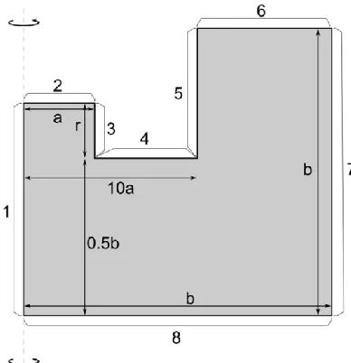
symmetry allowed a two dimensional (2D) axisymmetric cylindrical geometry to be used, as shown in Fig. 2. The electrode
radius, a in Fig. 2, was set to 70 nm and the amount of glass surround was set to 10a. These critical tip dimensions were
based on SEM measurements of the electrode used, which was done for each electrode studied. The size of the simulation, b
in Fig. 2, was set to 50 µm, and the recession depth, r in Fig. 2, varied. The concentration of FcTMA+ at the electrode
(boundary 2 in Fig. 2) was set to zero (c = 0). The glass area of the electrode (boundaries 3, 4 and 5 in Fig. 2) were set to no
flux ( c n 0), where n is the unit normal vector. The bulk solution (boundaries 6, 7 and 8 in Fig. 2) was set to bulk
concentration (c = 1 mM). Finally, the rotational symmetry axis (boundary 1 in Fig. 2) was set as a symmetry boundary
condition ( c n 0). Simulations were run on a personal computer (WindowsXP Pro 64 bit) using COMSOL Multiphysics
7
Fig. 2 The simulation domain (including dimensions and boundary labels), as described in the supporting text, for a 2D FEMsimulation of a recessed planar disk-shaped UME. Not to scale
Approach curves. Steady-state FEM simulations of a recessed disk-shaped planar UME, at an angle with respect to an
inert insulating substrate, and as a function of distance from the substrate, were carried out to quantify the effect of probe
angle on the distance-dependent current (approach curve) response. As above, equation (1) (Fick’s second law), describes the
mass transport of FcTMA+ to the electrode, but the incorporation of the probe angle breaks the rotational symmetry and
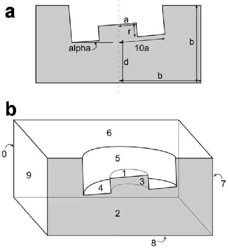
therefore a three dimensional (3D) simulation, with one plane of mirror symmetry, was used. Fig. 3 shows a 2D diagram of
the geometry, with probe dimensions, as well as the 3D simulation domain (which, again, is not drawn to scale), with the
[image:8.612.76.270.57.258.2]8
Fig. 3 (a) 2D representation of the geometry, including dimensions, of the angled recessed UME above a surface. (b)Thesimulation domain (including boundary labels), as described in the main text, for 3D FEM simulations of a recessed planar
disk-shaped UME above an insulating surface. Not to scale
The simulation domain is defined by the probe dimensions, shown in Fig. 3a, and described above. In addition, the probe
angle, alpha in Fig. 3a, and distance to the surface, d in Fig. 3a, are independent variables. The boundary conditions, shown in
Fig. 3b, of the FEM simulation are as follows: 1 is the electrode surface and the concentration is set to zero (c = 0); 2 is the
mirror symmetry plane and is set to have no normal flux ( c n 0); 3, 4 and 5 are the glass surrounds of the probe and are
set to have no normal flux ( c n 0); 6, 7, 9 and 10 are the bulk solution and set to the bulk concentration (c = 1 mM); and
8 is the insulating surface and set to have no flux ( c n 0).
Results and Discussion
Tip characterization. Pt-disk nanoelectrodes were fabricated reproducibly and reliably with the active electrode radius
typically in the range of 50 – 150 nm, exposed by FIB milling using the protocol shown schematically in Fig. 4a, in which a
series of cuts are used to produce an electrode with a well-defined (and relatively small) RG value. As formed,
nanoelectrodes were typically asymmetric, with an RG value between 20 and 30, and this is likely due to the position of the
Pt wire in the glass capillary during the sealing step. A typical nanoelectrode is shown end-on in the SEM micrograph in Fig.
4b. This asymmetry has recently been studied, and for RG values in this range does not have any significant effect on the
9
procedure, Fig. 4c shows an electrode that has been ‘shaped’ in the milling process to produce a tip of preferred geometry,i.e. smaller RG and more central location of the Pt.
Fig. 4 Side-view schematic of the FIB-milling procedure (a) showing ablation during the milling (i), a cut nanoelectrode (ii)
and reducing the RG of the cut electrode (iii). Top down view SEM micrographs of a Pt-disk nanoelectrode after FIB milling:
(b) of the cut surface after the procedure in (aii) and (c) an electrode shaped by FIB milling
The dimension of the exposed Pt surface can be characterized reasonably by measurement in the SEM. A typical SEM
micrograph used to characterize tip dimensions has been included for a single electrode in Fig. 4b. The tip shown has a 70 ±
10 nm radius, determined by SEM. A cyclic voltammogram (CV) for the oxidation of 1 mM FcTMA+ (0.1 M KCl) at a scan
rate of 200 mV s-1 is shown in Fig. 5a, which shows a characteristic steady-state response. By holding the tip in bulk solution
at the steady-state limiting potential, 0.45 V, a steady current of 2.51 pA was recorded. A non-recessed electrode would have
given a steady-state limiting current of 16.2 pA for this electrochemical reaction. If one naively assumed a planar disk
geometry, as has sometimes been done in the past, the tip radius would be calculated as 10 nm, using the steady-state limiting
current, iss, equation for a disk electrode (for an infinite RG [41]):
* 4
ss
i nFDc a, (2)
where n is the number of electrons transferred and F is Faraday’s constant (96 485 C mol-1). That nanoscale tips are often
recessed is increasingly recognized and additional characterization methods proposed to determine the geometry have been
proposed [42-44]. As highlighted herein, a recessed electrode is actually beneficial for application in IC-SECM as it serves to
[image:10.612.62.281.84.269.2]10
Fig. 5 (a) CV recorded for a 70 nm radius electrode (characterized by SEM) in 1 mM FcTMA+ and 0.1 M KCl, at a scan rateof 200 mV s-1. (b) Simulated steady-state diffusion-limited currents in bulk solution vs. Pt recession distance, r, in nm for a 70
nm radius planar disk electrode. Simulated results (blue) have been spline fitted (light blue) and theoretical results by Bond et
al. are shown (red dashed) [45]. The experimental diffusion-limited current, 2.51 pA, (green dotted) was used to determine r,
for this electrode. Inset shows key tip dimensions: electrode radius, a, glass sheath radius, rg, and Pt recession depth, r
The steady-state limiting current for the electrodes were always less than predicted for a non-recessed disk electrode based
on SEM measurements of the electrode radius, indicating that the tips were recessed to varying degrees [44-46]. In the case of
the tip considered above, the Pt radius as measured in SEM was ca. 7 times greater than the radius calculated from the
steady-state limiting current in the bulk. We need to consider that this discrepancy could partly be due to charging effects of the Pt
11
Tefashe and Wittstock, who studied micropolished Pt electrodes of sub-micron dimensions [47]. In their study, thenanoelectrode and glass sheath were coated in an ionic liquid to reduce such effects [48], yet a similar disparity was observed
to that herein (e.g. the radius measured in SEM was 348 nm, c.f. 53 nm calculated from iss). In our case, the electrodes were
grounded to the tip holder in the SEM to reduce charging effects.
We conclude that the main reason for the difference in electrode dimensions from SEM and voltammetry is that the
electrode is recessed, probably for reasons recently identified by Amemiya and co-workers [49]. Although we cannot rule out
some blockage of the active electrode as well, additional information from approach curves indicates that recession is the
main reason for the much diminished bulk current (vide infra). The extent of recession was estimated via FEM simulations, as
described above, using the well characterized electrode dimensions from the SEM measurements. For the tip shown in Fig.
4d, the model predicted a series of diffusion-limited currents in bulk solution for a series of recession depths, r, as shown in
Fig. 5b (inset). The relationship of limiting current of the tip in the bulk against Pt recession depth shown in Fig. 5b allowed
an estimate of 280 nm for the recession depth.
The effect of recession depth on the steady-state limiting current has been studied by others; Bond’s model works for
deeply recessed electrodes [45], whilst the model by Bartlett applies also to shallow recessed electrodes [46]. It can be seen
that the FEM model herein matches reasonably closely to the result by Bond et al., included in Fig. 5b [45]. AFM has also
been used to visualize the surface of nanoelectrodes [42], and white light vertical scanning interferometry can be used to
measure the recession of an electrode, although this is limited to electrodes of several to several tens of microns dimension
[43]. Our approach to measure the recession is fast and simple, based on the characterization by SEM and the
diffusion-limited steady-state current.
Approach curves. Importantly, by deploying IC-SECM with nanoelectrodes, we found that the detection of oscillation
amplitude damping is possible for small (nanoscale) tips. An amplitude setpoint of 95 % of that in the bulk was used for
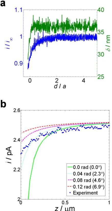
approach curves and imaging. A typical negative feedback approach curve to glass is shown in Fig. 6a, with the oscillation
amplitude, δ, shown in green. In the approach, damping is first observed when the current has fallen by ca. 5 %, i.e. just
beyond the noise level of ca. 2 % of the oscillation amplitude, although further extension of the tip into the surface leads to
the oscillation amplitude and tip current decreasing further. These needle-type nanoelectrodes possessed a large degree of
flexibility in the shaft of the tip, which was advantageous in allowing the tip to bend slightly, rather than snap, as it was
pushed against the substrate. Since the alignment between the tip and substrate was unknown, d / a was arbitrarily set to zero
12
Fig. 6 (a) Feedback approach curve to a glass (insulator) substrate with a 70 nm radius Pt nanoelectrode (characterized bySEM) oscillated at 70 Hz, δ = 36 nm in IC-SECM mode. The electrode potential was fixed at a value where 1 mM FcTMA+
in bulk solution underwent diffusion-limited oxidation at the tip electrode. The normalized current at the tip (blue) and
corresponding oscillation amplitude of the tip (green) are shown as a function of the tip-substrate separation where d/a = zero
corresponds to IC detection. (b) Simulated approach curves for tip angles with respect to the surface of 0 (green), 0.04 (light
blue dotted), 0.08 (pink dashed) and 0.12 radians (red dashed-dotted) against the experimental approach from part (a) (blue)
Using the known recession of the tip from the model shown in Fig. 6b, the same electrode was modeled approaching the
surface at different angles in order to find the misalignment between tip and substrate. Here, z = 0 μm corresponds to IC
detection (i.e. d ≠ 0 when alpha > 0), and the model did not consider tip bending. The low damping setpoint ensures tip
bending is minimized. Greater damping could lead to tip bending. IC-SECM detects IC, and there may be tip bending which
would occur to a greater extent, the higher the oscillation amplitude damping. To minimize this, we choose the smallest
[image:13.612.72.291.47.457.2]13
drop much beyond 90 % of the bulk current, Fig. 6b shows that the tip was misaligned to the substrate somewhere between0.04 and 0.08 radians, or about 3 ° or so, which appears reasonable and suggests that recession of the electrode is the main
reason for the greatly reduced currents in bulk compared to expectations based on a coplanar electrode of dimensions
identified in SEM.
A key component of the soft-tapping IC-SECM setup is the implementation of the piezo bender actuator, in which the tip
exerts less force on the sample. Using the manufacturer’s spring constants of 0.6 N µm-1 for the piezoelectric positioner used
in our previous setup (PI Hera P-621.ZCD) and 0.02 N µm-1 for the bender actuator implemented in this new setup (PICMA
P-871.112) we can estimate the forces applied by the tip on the sample of 3 × 10⁻³ N and 1 × 10⁻⁴ N respectively, based on a
displacement of 5 nm from the damping of the oscillation of the tip. These values are upper limits with these nanoscale tips
because tip bending may actually greatly reduce the force applied. Thus in this setup, the force of the tip on the sample, when
the tip is mounted on the bender actuator is ca. 3 % of the force when the tip is mounted directly on to the piezoelectric
positioner. The force exerted by the piezo bender actuator is of the same order as found for soft linear array imaging devices
[50, 51].
Imaging. A gold band array on glass was used as a substrate for IC-SECM imaging in feedback mode. An optical image of
the substrate is given in Fig. 7a. The 125 nm height of the gold band (Fig. 7b) was not detectable in the topography for the
area imaged by SECM, since the glass sheath surrounding the Pt nanoelectrode was ca. 3.6 µm. The AFM image shows that
the edge of the gold band is not perfectly straight due the lift off process in the fabrication of the sample, therefore a rough
edge was also expected in the electrochemical image. The radius of the Pt nanoelectrode used for IC-SECM imaging of the
14
Fig. 7 (a) Optical microscope image of the gold band sample, with a zoomed-in inset over the edge of a gold band. (b) AFMtopography image of the substrate with inset of a line scan. (c) View of the tip above the substrate prior to IC-SECM imaging.
(d) IC-SECM images of the edge of a gold band on glass, obtained using a 160 nm radius Pt disk electrode (80 Hz, δ = 39
nm, 1 mM FcTMA+). Forward scan in IC of mean tip current/bulk current (d), and reverse scan of mean tip current/bulk
current at constant separation of 300 nm (e)
Fig. 7d shows the feedback SECM image recorded with the tip in IC-mode, i.e. tracing the contours of the surface. When
the tip is over the gold substrate, there is some positive feedback leading to current values with respect to bulk that are
enhanced, i.e. i / i∞ > 1. Over the glass part of the substrate surface, negative feedback occurs, with diffusion to the tip
[image:15.612.76.560.46.515.2]15
with the surface. This image shows both lower resolution and lower deviation of local currents from the bulk current value,since the probe is further away from – and thus less sensitive to the nature of – the surface. The feature exhibiting negative
feedback in the reverse scan and positive feedback in the forward scan (at x = 1.5 μm, y = 1 μm) can be attributed to surface
contamination during the forward scan of the gold substrate by the tip. This clearly only affects a few pixels on one line in the
image, and with the development of hopping IC-SECM [52, 53], we will expect to reduce the amount of contact between the
tip and the substrate by > 99 %, which would overcome such problems in the future. Notice that the tip current over the glass
(insulator) in Fig. 7e was ca. 90 % of that in the bulk, which – although for a different tip – is in line with the approach curve
in Fig. 6. The resolution of the tip is clearly much greater than for a typical micron sized UME, since a change from gold to
glass occurs over a lateral distance of 200 nm at worst in Fig. 7d.
Conclusions
We have shown that nanoscale imaging is possible with IC-SECM, using Pt-disk electrodes fabricated by laser pulling, and
cut to a desired shape by FIB milling. The tips were found to be recessed, and the degree of recession was determined based
on the disparity between the steady-state limiting current and the apparent size of the electrode based on SEM measurements.
In addition, (mis)alignment between the electrode and the substrate surface was estimated based on the recession depth
determined, through approach curve measurements. The recessed nature of these tip electrodes is particularly useful for
IC-SECM in that it acts to protect the active electrode when it comes into contact with the surface. Although the results presented
herein are for amperometric tips over a model substrate, potentiometric probes could be used with this technique.
The implementation of the piezo-bender actuator was important in the realization of IC-SECM for nanoelectrodes. We
anticipate that this technique could be applied to image samples with features of nanometer dimensions, such as individual
carbon nanotubes, or low density single-walled carbon nanotube networks. The smaller force of the tip on the sample when
using the piezo-bender actuator, as compared to the z-piezoelectric positioner used in our previously described setup, could
allow for the imaging of softer samples, with greater topographical sensitivity. Future work could also consider the use of
hopping scanning [52, 53], to eliminate lateral forces on the tip during the imaging, while allowing the tip to move closer to
the sample by increasing the setpoint of the damping of the oscillation amplitude.
Acknowledgements
This work was supported by the Engineering and Physical Sciences Research Council (EPSRC) project studentship for
R.L. (Grant EP/H023909/1) and MOAC/DTC studentships for K.M. and M.B. We acknowledge support from a European
16
equipment used in this research was obtained through Birmingham Science City with support from Advantage West Midlandsand the European Regional Development Fund. We thank Robert B. Channon and Andrew J. Soulby for their early
contributions to the work. We are grateful to Dr. Alexander W. Colburn for designing and building the electronic