and Spin Transport in Organic Crystals
Subhayan Roychoudhury
School of Physics
Trinity College Dublin
A thesis submitted for the degree of
I, Subhayan Roychoudhury, hereby declare that this dissertation has not been
submitted as an exercise for a degree at this or any other University.
It comprises work performed entirely by myself during the course of my Ph.D.
studies at Trinity College Dublin. I was involved in a number of collaborations, and
where it is appropriate my collaborators are acknowledged for their contributions.
A copy of this thesis may be lent or copied by the Trinity College Library upon
request by a third party provided it spans single copies made for study purposes only,
subject to normal conditions of acknowledgement.
Subhayan Roychoudhury
Organic semiconductors offer several crucial advantages over their inorganic
counter-parts in electronic and spintronic applications. Besides offering structural advantages
such as variety and flexibility, organic semiconductors can be manufactured with cheaper
processes and at lower temperature. These promising potentials call for the
develop-ment of a complete theoretical framework, without any need for experidevelop-mental input, for
description of charge and spin transport in these materials. A possible strategy can be
to employ a multi-scale method where electronic structure is calculated with ab-initio
methods and the information so obtained is used to construct a material specific model
Hamiltonian. This Hamiltonian can then be solved with statistical techniques to extract
transport-related quantities, like mobility, spin-diffusion length etc. Since, in a real
de-vice, the organic semiconductor will be attached to conducting electrodes, the interface
between the two systems will play a crucial role in the device functionality. Keeping
these in mind, in this thesis, we attempted to calculate several important properties and
parameters of organic crystals related to electron and spin transport, both for the bulk
material and at the interface.
A modification of the popular Density Functional Theory (DFT) method known
as constrained DFT (cDFT) has been used to calculate the charge transfer energies
be-tween a graphene sheet and a benzene molecule absorbed on it. We have computed these
energy values for several modifications of the system-configuration and have
rational-ized the results in terms of classical electrostatics. Next, we have developed a method,
within the framework of calculations employing localized basis orbitals, to determine
the accurate forces when the energy of the system depends on a subspace population.
Such method, in conjunction with cDFT, has been used to evaluate the reorganization
energy of a pentacene molecule adsorbed on a flake of graphene. We have also developed
the excitonic DFT method for calculating the optical gap of materials with cDFT, by
confining certain number of electrons within a subspace of the Kohn-Sham
eigenfunc-tions. We have shown that this method predicts the optical gaps of organic molecules
with appreciable accuracy. We have also tried to extend this method to periodic solids.
As a step toward describing spin-related phenomena, we have extracted the
spin-orbit coupling matrix elements, which can be responsible for spin-relaxation in
or-ganic crystals, with respect to a set of maximally localized Wannier functions. We have
applied this on several materials and showed that the spin-orbit split band structures
calculated from the Wannier functions match those obtained directly with first principles
calculations. Since, in organic crystals, lattice vibrations play a major role at finite
tem-perature, we have extended the aforementioned work to include the effects of phonons.
To this end, we have calculated, with respect to the Wannier functions, the spin-phonon
coupling, namely the effect of various phonon modes on modification of spin-orbit
cou-pling. We have performed such calculation on a crystal of durene and showed that there
is no apparent correlation between the electron-phonon and the spin-phonon coupling
First and foremost, my sincere gratitude to Prof. Stefano Sanvito, my thesis su-pervisor and my role model. I have received guidance and freedom in a perfect blend
from prof. Sanvito. Besides having numerous invaluable discussions on physics, he has
taught me the art of solving problems by breaking up a big task into small manageable
ones. Above all, he has taught me the value of ethics, compassion and humility. I could
not have asked for a better advisor for my PhD.
I am greatly indebted to Dr. David D. O’Regan who showed incredible patience in giving thorough and detailed answers to millions of my questions. My interest
in first principles calculations is largely a result of countless extensive discussions with
Dr. O’Regan. The works presented in Chapter 5 and Chapter 6 resulted from discussions
with him.
I want to thankDr. Carlo Mottafor introducing me with great care to DFT and to the software siesta. Throughout the duration of my PhD, he has frequently
helped me with extremely valuable suggestions and discussions. Chapter 4 is a result of
collaboration with Dr. Motta.
I want to thank the past and present members of the Computational
Spintron-ics group at TCD for their friendship. In particular I would like to thank Dr. Ivan Runggerfor frequent help with smeagolandDr. Andrea Droghettifor suggesting
excellent books and other reading materials.
I am thankful toStefania Negrofor her efficient handling of all the adminis-trative works. I would like to express gratitude to Trinity Center for High Performance
Computing (TCHPC) and Irish Center for High End Computing (ICHEC) for letting me use their computational resources.
I am eternally grateful tomy parentsfor their unconditional love, support and encouragement. I want to thank my uncle, Dr. Saroj Maitywho greatly inspired me to study science. Very special thanks toDebottama, Sayantan, Deborashmi and Kaushambi, the best cousins in the world and to Anais, Gaurav, Jorge, Sagnik
and to all other friends in Ireland and India.
Finally, no amount of thanks will be sufficient to express my gratitude to my
Abbreviations
BVK Born-Von-Karman
c.c Complex Conjugate
cDFT Constrained Density Functional Theory
CT Charge Transfer
FBZ First Brillouin Zone
DFT Density Functional Theory
GGA Generalized Gradients Approximation
HK Hohenberg-Kohn
HOID Hybrid Organic Inorganic Device
HOMO Highest Occupied Molecular Orbital
SO Spin-Orbit
KS Kohn-Sham
LDA Local Density Approximation
LED Light Emitting Diode
LUMO Lowest Unoccupied Molecular Orbital
MLWF Maximally Localized Wannier Function
NEGF Non-equilibrium Green’s Function
NGWF Non-orthogonal Generalized Wannier Function
OLED Organic Light Emitting Diode
OSC Organic Semiconductor
PBE Perdew-Burke-Ernzerhof (exchange-correlation functional)
QP Quasi Particle
RKS Restricted Kohn Sham
TDDFT Time Dependent Density Functional Theory
UKS Unrestricted Kohn Sham
TB Tight Binding
1 Introduction 15
1.1 Electronics . . . 15
1.2 Spintronics . . . 19
1.3 Organic Electronics . . . 21
1.3.1 Structural Properties of OSCs . . . 22
1.3.2 Advantages of going Organic . . . 23
1.3.3 Fabrication of Organic Electronic Devices . . . 23
1.3.4 Applications of Organic Electronics . . . 24
1.4 Organic Spintronics . . . 27
1.5 Theoretical Description . . . 28
2 Modelling Transport in Organics 31 2.1 Experimental Results . . . 32
2.2 Band Like Transport . . . 33
2.2.1 Inclusion of Phonons in the Model . . . 33
2.2.2 Drawback of this model: Dynamic Disorder . . . 36
2.3 Polaronic Hopping Transport . . . 37
2.4 Model with Dynamic Localization . . . 38
2.5 Methodology for QUEST . . . 39
2.5.1 First-Principles Calculations . . . 41
2.6 Thesis Outline . . . 42
3 Theoretical Background 43 3.1 Energy Eigenstates of a Periodic Lattice . . . 43
3.2 Density Functional Theory . . . 47
3.2.1 Band Gap Problem . . . 54
3.3 Constrained Density Functional Theory . . . 60
3.4 Calculations based on the Kohn-Sham Scheme . . . 62
3.4.1 Exchange-Correlation Functional . . . 63
3.4.2 siesta . . . 65
3.4.3 onetep . . . 67
3.5 L¨owdin Population Analysis . . . 68
3.6 Lattice Vibrations . . . 71
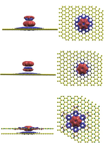
4 Charge Transfer Energy of Molecule on Substrate- Benzene Physisorbed
4.1 What Are the Quasiparticle Energies? . . . 76
4.2 Energy Level Renormalization . . . 79
4.2.1 Level Broadening . . . 80
4.2.2 Shifting of the Energy Levels . . . 81
4.3 The Quasiparticle Equation . . . 86
4.3.1 DFT and quasiparticle energies . . . 88
4.4 Computational Details . . . 90
4.5 Results . . . 93
4.5.1 Equilibrium Heights . . . 93
4.5.2 Dependence of the CT Energies on the Cellsize . . . 94
4.5.3 CT Energies as a Function of the Distance . . . 95
4.5.4 Effect Of Defects . . . 96
4.5.5 Effect of the Presence of Other Benzene Molecules . . . 99
4.5.6 Classical Image Charge Model . . . 101
5 Constrained DFT with accurate ionic forces applied to the reorgani-zation energy of graphene-adsorbed pentacene 105 5.1 Introduction . . . 105
5.2 Physical Problem Investigated . . . 107
5.3 Method . . . 108
5.3.2 Procedure for the Calculation . . . 114
5.4 Results . . . 117
5.4.1 Test of the Forces on Isolated Pentacene . . . 117
5.4.2 Reorganization Energy of Graphene Adsorbed Pentacene . . . 119
5.5 Conclusion . . . 126
6 Excitonic DFT: A Constrained DFT Based Approach For Simulation of Neutral Excitations 127 6.1 Background . . . 127
6.1.1 The Concept of Exciton . . . 128
6.1.2 State-of-the art . . . 131
6.2 The Excitonic DFT Method . . . 134
6.3 Results . . . 137
6.3.1 Optical gap of Molecules . . . 137
6.3.2 Optical gap of Periodic System . . . 151
6.3.3 Double Excitation of Beryllium . . . 155
6.4 Conclusion . . . 157
7 Calculation of the Spin-Orbit Coupling Terms from Maximally Local-ized Wannier Functions 159 7.1 Maximally-Localized Wannier Functions . . . 161
7.2.1 General idea . . . 163
7.2.2 Numerical Implementation . . . 164
7.2.3 Workflow . . . 167
7.3 Results and Discussion . . . 168
7.3.1 Plumbane Molecule . . . 168
7.3.2 Lead Chain . . . 173
7.3.3 Carbon Chain . . . 174
7.3.4 Methane Chain . . . 178
7.3.5 Triarylamine Chain . . . 178
7.3.6 3D structures: FCC lead and PhBr2C6Br2 . . . 184
7.4 Conclusion . . . 187
8 Calculation of Spin Phonon Coupling with respect to Wannier Func-tions 191 8.1 One Dimensional Pb Chain . . . 194
8.2 Durene Crystal . . . 199
8.3 Approximated Wannier Basis Set . . . 206
8.4 Conclusion . . . 209
9 Conclusion 211
A Dependence of the Eigenvalue on Matrix Size and the Off-Diagonal
B Spin-phonon coupling matrix elements of a Pb chain calculated with
respect to ‘p’ orbitals 219
Chapter
1
Introduction
The cornerstone of modern technology is the ability to process and store information
with machines. It would be hard to think of any aspect of life where one does not use
such technological advances. The most common format for processing and storing data
by machines is the binary format in which all the data are represented as combination of
two numbers (0 and 1) each occupying the storage space of one bit. In the basic electrical
circuit used in such technology, these two numbers can be represented as currents of
two different magnitudes, one high and one low. Devices, which can work with binary
data in form of electrical responses, are broadly classified as electronic devices.
1.1
Electronics
The field of electronics concerns the control and manipulation of electrons in devices
made of certain materials, which possess properties facilitating such actions. The
sci-ence and technology of electronics form one of the most ubiquitous and indispensable
backbones of modern life.
• Integrated circuits or ICs, made up of numerous transistors, are the primary com-ponents of the processing units responsible for thelogic operations of almost all
devices related to computing such as computers, mobile phones, tablets,
calcula-tors etc.
• LED lights, used extensively for their versatility and low energy consumption, are electronic elements which, when activated, act as light sources.
• Traditional solar cells, which convert light into electric current, are essentially large area photodiodes, namely they are electronic components in which light can
reach the sensitive part of the device resulting in the generation of an electrical
response.
• Sensors, which are used to detect physical (light, temperature, magnetic field, gravity, vibration, motion, stretching, etc.) or chemical (toxins, glucose level,
oxy-gen level, hormones, nutrients, etc.) properties depend on electronic components
for their operations.
• Amplifiers, which increase the power of any electrical signal and find widespread application in speakers, are made with electronic components.
Among the applications listed above, the first one, namely logic is probably
the most widely used. In this case, the basic principle of operation is that of detecting
the change in electric current in the device as a function of an external electric stimulus.
For instance, in a transistor the current between the source and the drain changes as the
gate voltage is changed and the detection of the change of the former as a function of the
latter forms the basis of logic operations. Fig. 1.1 shows the basic structure and working
principle of the simplest electronic device, a p-n junctiondiode [1]. It consists of an n
-type material, known asdonor, which is rich in free electrons very weakly bound to the
ions, and ap-type material, known asacceptor, which has many vacancies in its valence
states, i.e. which, in other words is rich in free holes. When an initially charge-neutral
donor is brought into contact with an initially charge-neutral acceptor, the free electrons
from the former diffuse into the latter to fill the vacant positions, resulting in a negatively
charged acceptor and a positively charged donor. The migrated charges accumulated
acceptor and an associated potential called the barrier potential. This prevents further
charge transfer, creating what is known as a depletion region. Thus, in this condition
there is no current in the device. In the reverse bias condition a positive (negative)
potential is applied to the donor (acceptor), thus enhancing the barrier potential even
further and strengthening the condition of no charge flow. However, in the forward bias
condition, when one applies a positive bias voltage to the acceptor and a negative bias
voltage to the donor, one can create an electric field opposite to the one responsible for
the creation of the depletion layer. Thus, the bias reduces the width of the depletion
layer and the barrier potential. When the bias is strong enough, charge carriers overcome
the barrier potential and current flows through the p−n junction from the acceptor
region to the donor region. From the description presented above, it is clear that such
devices can be used as switch between two current states representing the two binary
numbers.
Considering the requisite properties, we see that, in order to qualify as a donor
or an acceptor, a material needs to have unique electronic properties which allow for
the desired control of electrons in them. These materials form the active component
of an electronic device. As such for the donor, one needs a material which is rich in
free electrons but not in free hole and for the acceptor one needs a material possessing
the exact opposite characteristics. This is done by choosing a crystal where the energy
difference between the highest occupied and the lowest empty electronic bands does
not vanish, as in metals nor is as large as in insulators. Such materials, which are
ubiquitous in almost all electronic devices are known as semiconductors [2]. In order to
create a donor material, a semiconductor is doped with impurities so that an additional
filled level is created very close to the conduction band just below it. Thus, the Fermi
level is now positioned between this additional level and the valence band, and at room
temperature, electrons can move into the conduction band giving rise to conduction. For
an acceptor material, the pristine semiconductor is doped to create an additional empty
donor acceptor donor acceptor donor acceptor
No Bias Reverse Bias Forward Bias
[image:18.612.68.491.112.585.2]Potential
Figure 1.1: p−njunction diode: Top panel shows an unbiasedp−n junction diode and
its depletion region. Bottom panel shows potential profile of the p−n junction under
different conditions of bias; (From left to right) zero bias, reverse bias and forward bias,
1.2
Spintronics
In general, a magnetic field is less effective than an electric one in producing electronic
motion. However, the magnetic properties of a material are associated with the spin
of an electron and consequently in many cases an electric stimulus can be replaced by
a magnetic one, provided that one exploits the spin degree of freedom, even if in an
indirect fashion, in the detection process. The resistance faced by a charge carrier is
independent of its spin in a non-magnetic material. However, if the material is magnetic,
then the resistance typically depends on the relative orientation of the carrier spin and
the local magnetization [3]. This inspires one to create the spin valve [4], which is a
prototypical device for the interesting sub-field of electronics known as spin-electronics or
spintronics [5]. The simplest spin valve consists of two layers of ferromagnetic materials
sandwiching a non-magnetic spacer [6]. Usually, one of the ferromagnets have a fixed
magnetization, while the magnetization of the other one is free to change. If both the
ferromagnets have the same orientation of magnetization (say, up), then electrons with
up (down) spin face very low (high) resistance in both of them. Here we invoke Mott’s
idea [3] that the current is carried by two parallel spin channels, one for up spin and one
for down. Thus, in presence of a voltage difference, a current comprising predominantly
up spin electrons will flow between the two layers. However, if the magnetizations of
the two ferromagnets are opposite of each other, then an electron with any spin will
face a high resistance in one layer and a low resistance in another layer. Now, if the
resistance of the spacer is not too high, then the three layers can be thought of as
resistors in series and for each spin channel, the net resistance will be the sum of the
individual contributions of the three layers. In the parallel configuration there will be
high current (because of the up spin electrons which face very low net resistance) but
in the anti-parallel configuration there will be very low current (because all electrons
face significant net resistance). Thus by knowing the magnetization direction of the
fixed layer and by measuring the current flow, one can determine the magnetization of
the free layer. This is smartly exploited in the read head of a hard disk drive, where
Figure 1.2: Schematic diagram showing a GMR based spin-valve where the spacer has
low resistance. The arrows denote spin direction of the carrier. If, as shown in the left
panel, both the ferromagnets have the same direction of magnetization (say up), then
carriers with up (down) spin face very small (large) resistance in both ferromagnets.
Therefore, a current comprising spin up carriers flows from one ferromagnet to the
other. However, if, as shown in the right panel, the ferromagnets have opposite spins,
then carriers of either spin will experience high resistance in one ferromagnet and low
resistance in the other one, resulting in low current. In the schematic diagram for
effective resistance, the top (bottom) series represents resistance faced by spin up (down)
carriers while the thin and the thick lines denote low and high resistance, respectively.
According to Mott’s idea, the two parallel resistors for the two spin channels determine
be altered by the stray magnetic field of the hard disk. Today spintronics has found
widespread application in the field of data storage as an integral component of the hard
disk drives.
One of the crucial points related to spin-valves is the choice of material used
as spacer. Historically, in giant magneto-resistance (GMR) [7, 8] devices, a metal was
used as spacer so that no additional resistive effect was introduced on the spin-polarized
charge carriers. In contrast, in the tunnelling magneto-resistance (TMR) case [9], an
insulator is used as spacer so that instead of spin injection into the spacer, spins tunnel
from one ferromagnet to the other. Yet another possibility is that of using
semicon-ductors [10, 11] as spacers. However, since semiconsemicon-ductors have considerable resistance,
which is equal for carriers of both spins, the net resistance of a spin-valve made with
semiconductor spacers, depends very weakly on spin. This conductivity mismatch
prob-lem can be circumvented by adding layers of spin-selective large barriers on both sides
of the semiconducting spacer [12]. The main motivation behind using semiconductors
as spacers is the idea of having a common platform for logic operations (which use
semi-conductor based devices) and information storage. Besides, the electronic properties of
semiconductors can be changed to a large extent as desired by tuning their electronic
structure, which is a decided advantage.
1.3
Organic Electronics
Although inorganic semiconductor materials have traditionally been at the centre of
focus for electronics and spintronics, a number of experimental and theoretical studies
have propelled attention and interest in semiconductors made up of organic
materi-als [13, 14, 15, 16]. Besides holding some key advantages related to properties and
man-ufacturing, organic materials come in an infinite variety of shapes, forms and electronic
structures which have endless possibilities for tuning and modification [17]. Organic
semiconductors (OSCs) can be classified in two broad categories:
structure and small molecular weight held together by Van der Waals interaction.
Typical examples include crystals made of tris(8-hydroxyquinolinato)aluminium
(abbreviated as Alq3), copper phthalocyanine (abbreviated as CuPC), rubrene,
durene, pentacene etc [18].
2. Organic polymers, which are mostly amorphous long chain-like molecules com-posed of repeated units known as monomers. Polymers like polyfluorene,
polypheny-lene vinypolypheny-lene (PPV), polythiophene etc. fall under this category.
There are vast differences among the general properties of organic and inorganic
semiconductor materials. For example, the mobility of a conventional p-doped silicon
is about 450 cm2V−1s−1, whereas that of rubrene crystal, one of the best conductors
among the OSCs, is approximately 10 cm2V−1s−1 [19]. The differences in properties between OSCs and their inorganic counterparts suggests that the goal for application
of organic electronics can not be that of displacing the existing inorganic counterparts
but can be one of creating a separate niche area of its own [20].
1.3.1
Structural Properties of OSCs
A common structural property shared by most organic semiconductors is the presence of
carbonσ and π bonds. The σ bonds are usually in the form of a planar sp2 structures.
The remaining pz orbitals, which are perpendicular to the plane containing the bond,
take part in forming π bonds between adjacent molecules (in crystal) or monomers (in
polymer). These π-bonds play significant roles in the charge conduction in OSCs. The
pz orbitals from adjacent units form two delocalized levels- a π bonding level which
contributes to the valence states and aπ∗ antibonding level contributing to the conduc-tion states. Therefore, these π orbitals are usually responsible for charge transport in
crystals or polymer.
Unlike typical inorganic semiconductors, which are held by covalent bonds
whose strength as a function of distance (R) goes as R12, the crystals or polymers in
goes as R16. Therefore, OSCs are much softer and more fragile compared to the
inor-ganic counterparts. Also, because of the weak bonding between individual units, charge
carriers tend to be more localized on individual molecules. Therefore, charge transport
in OSCs does not occur exclusively through delocalized band-like motion, but there
is usually a significant contribution of localized hopping of carriers from one unit to
another. This localization is also true for the neutral excitations, which are typically
tightly bound Frenkel excitons confined to individual molecules.
1.3.2
Advantages of going Organic
The biggest advantages that OSCs offer over their inorganic counterparts are their
mechanical flexibility, light weight and possibility of synthesis at low temperature [21].
Over the years, several low cost methods have been developed for fabricating
OSC-based devices. An important advantage of organic electronic devices is that they can
be manufactured at much lower temperature than that required for their inorganic
counterparts. Thus, their production requires much less power and expenses and incurs
less health-hazards. In particular, several possibilities for large area deposition and
patterning for organic semiconductors have been demonstrated [20]. One huge advantage
in organic electronics is the fact that organic thin films can be deposited on several
inexpensive substrates like plastic, glass or metal foils- without having to worry about
lattice matching conditions as with inorganic semiconductors.
1.3.3
Fabrication of Organic Electronic Devices
Thin films based on organic molecular crystals are formed usually with vapour-phase
deposition techniques [22, 23]. In the Vacuum Thermal Evaporation (VTE) method, the
source material is placed several centimeters below the substrate in a vacuum chamber.
Heating of the source results in deposition of the film on the substrate. It is possible to
deposit multiple layers with varied functionalities on the substrate and hence VTE is the
electronics. However, one of the biggest drawbacks of VTE is the difficulty experienced
in maintaining a uniform rate of deposition. In a promising alternative technique called
Organic Vapour Phase Deposition (OVPD) [24, 25], a hot walled vessel filled with an
inert gas is used to place the source in. On heating the source, the gas saturates with
the source material and deposits it on the cooled substrate. To manufacture an actual
device, it is usually required to locally pattern the deposition on the substrate. This
can be done at the time of deposition with Organic Vapour Jet Printing (OVJP) [26]
where the evaporated organic molecules pass through a nozzle before being deposited
on the substrate close to its tip. Several techniques [27, 28] are available for patterning
the organic film after deposition.
Polymeric thin films are usually deposited with solution based techniques where
the deposition takes place in the presence of a substrate (instead of being in vacuum
or in an inert gas) which is fully evaporated after deposition. In this case patterning is
possible with ink-jet printing [29, 30, 31] which promises unprecedented cost-effective
efficiency. More recently, several complimentary methods for solution based processing
have been proposed for molecular crystals as well [32, 33, 34].
1.3.4
Applications of Organic Electronics
Among the practical uses of organic electronic devices, Organic Light Emitting Diode (OLED) [15, 35] in display panels is by far the most widespread. OLED-based displays for phones, tablets and monitors are routinely manufactured in large scale
-creating a huge commercially successful industry. Unlike liquid crystal displays, OLED
displays function without a backlight and therefore have better power efficiency and can
show deeper black levels. Since OLED pixels emit light directly, they have a greater
contrast ratio and wider viewing angle compared to LCD screens. The response time
for an OLED-based display device can be 1000 times faster than that of their LCD
counterparts. Besides, OLEDs are thin, lightweight and flexible devices and therefore
enjoy multiple advantages in technological applications. In a typical bilayer OLED an
two electrodes- all deposited on a substrate. The cathode and the anode injects electrons
and holes into the semiconductor respectively. Since, in most cases the semiconductor
has better mobility for holes, an electron and a hole combine close to the emissive layer
to create a bound electron-hole pair, known as an exciton which eventually drops to a
lower energy state with emission of electromagnetic wave with frequency in the visible
spectrum.
Owing to the advantages of organic electronics, especially due to the cost
ef-fective fabrication technologies of large volume electronic devices, OSCs offer an
alter-native [36, 37] to their inorganic counterparts in photovoltaics. Even though there has
been no large commercial production of Organic Photovoltaic Cells(OPV cells), due to two major drawbacks, (i) very low efficiency (10%) compared to silicon solar cells and
(ii) the possibility of environmental degradation, these are subjects of active research
in both the theoretical and experimental community. A typical OPV cell consists of
an electron donor and an electron acceptor layer between two electrodes. One usually
places additional blocking layers between the semiconductor and the electrodes. A
pho-ton from the sunlight excites an electron in the donor region. The resulting excipho-ton
is broken up into a free electron-hole pair by the effective field of the semiconductor
heterojunction. The electron (hole) travels across the acceptor (donor) to be collected
at the metal electrode and to feed into the circuit, thereby generating current flow.
Field Effect Transistors (FETs) made of OSCs are a common reality. Even
though an Organic Field Effect Transistor(OFET) [38, 39, 40] is far from being us-able in logic operations (due to low carrier mobility in organic crystals) it has promising
features for other applications namely, as backpane of OLED displays, imagers,
mechan-ical sensors, etc. An OFET follows the architecture of a Thin Film Transistor (TFT),
where the source and the drain electrodes are deposited on the semiconductor channel,
which is separated by an insulating layer from the gate electrode. As in any FET, a
voltage between the gate and the source electrodes drives a current between the source
Property Organic Semiconductor Inorganic Semiconductor
Mechanical
Property
Higher mechanical flexibility, softer
structure, lighter weight
Less flexibility and softness,
heavier material
Production Easy and low-cost production Expensive and labour intensive production
Mobility Low mobility Much higher mobility
Variety
Large range of variety in structure
and property
Less variety in structure and
property
Temperature Narrow window of optimum temperature for operation
Wider window of optimum
temperature for operation
Spin
relaxation
time (T2)
[image:26.612.63.534.232.525.2]Lower spin relaxation time Higher spin relaxation time
Table 1.1: Comparison of properties of organic semiconductors with the inorganic
1.4
Organic Spintronics
As mentioned before, using inorganic semiconductors as spacer materials in spintronic
devices offers the advantage of having a single platform for processing and storage of
data. The ease of low-cost production of OSCs is a motivation enough to explore
the possibility of incorporating them in spintronic devices. A desirable quality for a
spacer material is that it should maintain the initial spin-polarization of the injected
carrier as much as it can. In other words, the scattering of spins inside the spacer
should be minimal. Since the main agents of spin scattering, namely spin-orbit coupling
and hyperfine interaction are both low in OSCs [19], organic materials usually have
very long spin-relaxation time, τs. This is a measure of the average time taken for
spin relaxation.1 This makes OSCs attractive candidates for research on spintronic
applications. There are several questions related to such research and they prove to
be challenging for experimentalists and theoreticians alike [41]. Since the mobility in
OSCs is much lower than that of typical inorganic semiconductors, it is debated whether
the transport of carriers from one ferromagnet to the other occurs by injection (as in
GMR) or by tunnelling (as in TMR). Recent experiments have shown definitive evidence
in support of spin-injection in CuPC [42] and Alq3 [43] crystals. Experiments have
also shown a negative magnetoresistance [44] in organic spin valves, i.e. the resistance
diminishing with increment of an applied magnetic field. This apparently surprising
experimental evidence has been explained [45] as the result of a renormalization of
the widened molecular states at the metal-OSC contact. Such states hold the key
to determining the spin-polarization of the injected current. This provides additional
challenge to the modelling of these molecular levels and thereby predicting the current.
Finally, a crucial question, which is yet to be answered is: which interaction,
spin-orbit coupling or hyperfine interaction, is responsible for spin-relaxation in OSCs? As
1Here, it is worth mentioning that the spin-relaxation time can pertain to two very distinct
phenom-ena. In the context of nuclear magnetic resonance, the longitudinal spin relaxation time, T1is the time
needed for the spin to reach equilibrium with its surroundings. In contrast, the transverse relaxation
time, T2is the time associated with relaxation of an injected spin from one configuration to the other.
conflicting experimental evidence is currently present in support of both [46, 47], it is
conjectured that the relative dominance of one over the other depends on the specific
OSC used.
1.5
Theoretical Description
The above discussion points to the need for a complete theoretical description of charge
and spin transport in semiconductor devices made of organic materials. Since a
typ-ical organic electronic device consists of an OSC crystal sandwiched between metallic
electrodes, anab initio theory (i.e. one for which the only required inputs are the
exper-imental conditions and the structure of the materials involved) for such a real Hybrid
Organic/Inorganic Device (HOID) would be of great interest. Of particular importance
will be a general transport theory for an HOID where the crystal ranges in length from
10-100 nm since this is the typical length-scale for exciton recombination [48] or spin
relaxation [19]. The unique structural properties of OSCs, which in many cases serve
as the advantages of organic electronics, make such theoretical description of transport
extremely difficult and challenging. This can be attributed to mainly two reasons:
1. Since OSCs are composed of well-separated and weakly interacting molecules,
charge carriers tend to be localized and the delocalized band-like transport seen in
covalently bonded inorganic semiconductors is not observed. In organic crystals,
charge transport likely occurs as a mixture of band-like transport and hopping
of localized carriers. The relative contribution of the two mechanisms depend
largely on the particular crystal and experimental conditions such as the
temper-ature. This makes it very difficult to formulate a general, computationally viable
framework valid across all regimes of transport in such materials [49].
2. The weak intermolecular attraction also results in the abundance of vibrational
modes at finite temperature. These vibrational motions play a crucial role in
DFT in conjunction with the Non-equilibrium Green’s Function (NEGF) method
inadequate in their treatment.
In addition, in a real HOID, the effect of injection of charge/spin carrier from
the electrode into the OSC must be fully incorporated within the theoretical model.
Such injection in general depends heavily on the electronic structure at the interfacial
region between the metal and the crystal making the modelling of transport a
multi-faceted problem. The most promising general framework in this regard is to calculate
the accurate electronic structure of the system in question: including both the
semi-conductor crystal and the metal-organic interface. Then one can construct a model
Hamiltonian for the system, using parameters obtained from the electronic structure
calculations. By solving this model Hamiltonian, one can obtain the observables
asso-ciated with transport in the real HOID.
In the next chapter we will present a brief review of the existing models for
describing charge transport in OSCs in various limits. This provides an idea of the state
Chapter
2
Modelling Transport in Organics
Modelling charge transport in organic materials is as challenging as it is important. The
density functional theory+ Non-equilibrium Green’s Function (DFT+NEGF) scheme [50,
51], one of the most popular techniques for the theoretical description of transport,
proves to be inadequate in treating real organic devices for several reasons. This fully
quantum mechanical treatment is limited to devices comprising a few hundreds of atoms.
A real Hybrid Organic Inorganic Device (HOID) of 10-100 nm length can contain about
10,000-10,000,000 atoms rendering it computationally intractable for the DFT+NEGF
scheme. Secondly, this scheme is designed for phase-coherent transport. Although
inelastic effects can be included perturbatively, any system where the transport is
dom-inated by the vibrational degrees of freedom are off-limits for this method. Organic
crystals are typically composed of molecules loosely bound to each other by weak Van
der Waals’ force. This is in contrast with common inorganic semiconductors in which
the bond is typically a much stronger covalent bond. Since the molecules are weakly
bound, at finite temperature they vibrate with large amplitude about their equilibrium
position. This means that at finite temperature, organic semiconductors typically have
a large number of phonons in them. The electrons and the phonons influence each other
and their combined effect is described with a collective quasiparticle named polaron.
The interplay between ionic and electronic motion makes the theoretical modelling of
transport in organic semiconductors much more challenging and complicated than in
their inorganic counterparts. Thus, the DFT+NEGF scheme is not a wise choice for
such systems. Furthermore, in organic crystals the nature and effects of impurities,
which play a crucial role in charge transport, are usually very different [52]. All these
differences suggest that the common methods used for describing transport in inorganic
semiconductors can not be used in their unmodified forms for organic crystals.
We begin this chapter with a very brief discussion of experimental observations.
This will help us to appreciate the merits and drawbacks of various state-of-the art
theoretical transport models that follow. Here we shall focus our attention mainly on
transport of charge because, once the mechanism of transport and a viable method
for its treatment are established, such method can be largely transferred to the
spin-dependent case with an appropriate change in the Hamiltonian. Finally we shall provide
a short description of the aims of a project proposed by Prof. Stefano Sanvito titled
QUantitative Electron and Spin Transport theory for organic crystals based devices
(QUEST), of which this thesis forms an integral part.
2.1
Experimental Results
The experimental investigation of charge transport in OSC is challenging due to the
difficulty in obtaining ultra-pure semiconductor crystals without defects. Early
inves-tigations involved mostly impure crystals and demonstrated activated transport [53],
i.e. one where the mobility increases with temperature. However, more sophisticated
measurements have attributed such behaviours mostly to the presence of defects.
Exper-iments with highly purified pentacene [54], tetracene, rubrene and functionalized
pen-tacene [55] have shown a temperature dependence of mobility that goes like µ ∼ T−n.
Since such relations are typical of delocalized band like transport, it is natural to think
of such transport to be prevalent in organic semiconductors also. However, electron spin
resonance experiment on a thin film of pentacene at room temperature have shown that
the carriers are localized within approximately 10 molecules [56]. Furthermore, a recent
sig-natures of charge localization despite displaying a reduction of mobility with increasing
temperature [57]. All these evidences seem to point, at least for highly purified and
or-dered organic crystals, to the apparently contradictory phenomenon of charge transport
with localized carriers where mobility decreases with increasing the temperature.
2.2
Band Like Transport
In any ideal periodic crystal structure, the energy eigenstates are delocalized Bloch
states,ψnk, characterized by their crystal momentum,k. A Bloch state can be expressed
as a linear combination of plane waves with wave numbers differing by translations in
the reciprocal lattice.
|ψnki=
X
G
Cn(k+G)|k+Gi (2.1)
whereGdenotes reciprocal lattice vectors and|qidenotes a plane wave with wavenum-ber q. This is discussed in detail in Section 3.1.
2.2.1
Inclusion of Phonons in the Model
As mentioned earlier, in organic crystals the vibrational degrees of freedom play an
important role in charge transport. In quantum mechanics, the lattice vibrations are
taken into account in terms of bosonic quasi-particles known as phonons (see Section 3.6
for a detailed account). Since the crystal in composed of weakly bonded molecular units,
we intend to use a tight-binding (TB) Hamiltonian which is written with respect to
localized basis orbitals (see observation 4 in section 3.1). The TB hamiltonian can be
ˆ
H=X
m
ma†mam+
X
m6=n
γmna†man+
X
mnQ
~ωQgQmn(b
†
Q+b−Q)a
†
man+
X
Q
~ωQ(b
†
QbQ+
1 2).
(2.2)
Here ωQ is the angular frequency of the phonon mode Q (here Q includes both the
phonon wavevectorqand the branchλ),b†Q (bQ) is the creation (annihilation) operator
for phonon mode Q and gQmn is the electron-phonon coupling. In the above equation,
the first term corresponds to the on-site Hamiltonian, the second term is the hopping
term, the third term denotes the electron-phonon coupling Hamiltonian, while the fourth
one denotes the purely phononic part of the Hamiltonian. We can see that the terms in
the above equation can be regrouped in the following manner:
ˆ
H =X
m
m+
X
Q
~ωQgQmm(b
†
Q+b−Q)
!
a†mam (2.3)
+X
m6=n
γmn+
X
Q
~ωQgQmn(b†Q+b−Q)
!
a†man (2.4)
+X
Q
~ωQ
b†QbQ+
1 2
.
Except for the last term, which does not act on the electronic degrees of
free-dom, this looks like a TB hamiltonian with the onsite and hopping terms modified
due to the presence of phonons. The phononic terms modifying the on-site energy
and the hopping are known respectively as the Hosltein term and the Peirls term. In Eq. (2.3), the electronic and phononic degrees of freedom are coupled. Therefore,
the goal here is to decoupled them to make further progress. By applying a canonical
H →H˜ =eSHeS†
where
S =X
mn
Cmna†man,
Cmn =
X
Q
gQmn(b†Q−b−Q) (2.5)
one can obtain, for low electron density the transformed Hamiltonian, written with
respect to the previous electronic creation and annihilation operators,
˜
H =X
mn
˜
Emna†man+
X
Q
~ωQ(b
†
QbQ+
1 2)
where,
˜
Emn= (eCEe−C)mn,
Emn=mn−
X
Q
~ωQ(gQg−Q)mn. (2.6)
It is important to note that unlikemn or Emn which are numbers, ˜Emn is an
operator since it contains the phonon creation and annihilation operators. It is difficult
to proceed further with this exact Hamiltonian. However, one can approximate the
operator terms ˜Emn with their thermal averages hE˜mni. This makes the electronic and
the phononic operators completely decoupled in the Hamiltonian of Eq. (2.6). Clearly,
the term proportional to hE˜mni for (m 6= n) acts as the modified hopping parameter
and gives a measure of the electronic bandwidth in presence of phonons. A calculation
of these terms for a given finite temperature shows that the presence of the non-local
electron-phonon coupling term results in a narrowing [58] of the polaronic bandwidth
compared to the bare electronic one. A similar thermal averaging of the phononic
operators can be performed in the context of transport calculation [59] and an expression
has been used successfully for modelling transport in ordered organic crystals at low
temperature [60, 61].
2.2.2
Drawback of this model: Dynamic Disorder
The narrowing of the bands due to the presence of phonons implies an increment of the
effective mass of charge carrier and consequently a reduction of the mobility. Therefore,
at sufficiently high temperature, the mean free path of the carrier becomes comparable
with intermolecular distances rendering the assumption of delocalized bandlike transport
inapplicable.
Looking at it from a slightly different perspective, one can see that replacing the
terms involving the phonon operators by their thermal averages is equivalent to assuming
that the onsite energy and hopping (which are numbers) of the zero temperature TB
Hamiltonian can be modified (replaced by other numbers) to take into account the effect
of phonons. In other words, we assume that at all instants the crystal is still periodic
and on average, it is sufficient to replace the tight binding Hamiltonian in absence of
phonons with another one with different parameters in order to describe the temperature
dependence of the mobility. However, at a high temperature the lattice sites oscillate
about their equilibrium positions with large amplitudes. Due to the presence of a large
number of phonon modes in the system, the thermal motion of the various sites are highly
uncorrelated resulting in a loss of general periodicity of the system [62]- a phenomenon
known as dynamic disorder. Thus, at each instant, the coupling between different lattice sites varies largely and the Hamiltonian becomes disordered. Such a disordered
system can not be treated with a delocalized Bloch wave and thereby calls for new
2.3
Polaronic Hopping Transport
We have seen that dynamic disorder introduced by lattice vibrations makes a crystal
non-periodic and treatment of the system with delocalized Bloch states becomes inadequate.
Such disorder results in localization of the charge carrier over one or a few lattice sites.
Although it doesn’t take the dynamic disorder into account, a popular method for
treating transport of localized charge at a finite temperature T is through the hopping
of such localized charge carriers [63, 64] (small polaron) from one site m to another n.
The rate kET of such a charge transfer is given by Marcus’ theory [65]:
kET = |
γmn|2
~ r
π λkBT
exp
−(λ+ ∆G
0)2
4λkBT
(2.7)
where, kB is the Boltzman constant, λ, known as the re-organization energy is the
change in energy corresponding to the ionic re-arrangement following the charge transfer
and ∆G0 is the change in Gibbs’ free energy corresponding to the same. Since the
on-site energy in the TB picture (for the HOMO/LUMO) is a measure of charging energy
of the site and since the local electron-phonon coupling provides a measure of the
mod-ification of this on-site energy due to the lattice vibrations, the re-organization energy
can be thought of as an alternative way of charaterizing local electron-phonon coupling
strength. This description ignores the non-local electron-phonon coupling (Peierls term)
and the resulting dynamical disorder. It can be shown [49] that for a system without
dynamic disorder, for γ ≥ λ2, there can not be any localized small polaron at any
tem-perature and therefore the concepts of hopping and rate equation become moot. One of
the most important limitations of this approach is its prediction of thermally activated
transport- i.e. increment of mobility with temperature, which is in contrast with
exper-imental results on highly purified and ordered organic crystals, in which the mobility is
2.4
Model with Dynamic Localization
The preceding paragraphs suggest that though at very low temperature, the transport in
a highly pure and ordered organic crystal can be considered to be band like, for a more
general case, an effective model for charge transport in pure organic crystals at finite
temperature should be able to predict a reduction in mobility with increment in
tem-perature without assuming transport through delocalized Bloch states. An interesting
procedure, developed by Troisi et al. [66, 67] solves this problem by using a semiclassical
time-dependent Hamiltonian which treats the electronic and ionic degrees of freedom
with quantum mechanical and classical approaches respectively. For the simplest case of
a one-dimensional periodic system with nearest neighbour interaction and one localized
orbital per site, the Hamiltonian takes the form:
H =X
j
[−γ+g(uj+1−uj)] (|ji hj+ 1|+|j + 1i hj|) +
X
j
1 2 mu˙
2
j +Ku
2
j
, (2.8)
where the time-dependent quantityuj denotes the displacement of thej-th site from the
equilibrium position at any instant,γ is the average hopping parameter between sites, g
is the electron-phonon coupling andmandK are the mass and the force constant of the
oscillator respectively. Clearly, here the first sum on the right hand side denotes the
elec-tronic Hamiltonian Hel (including electronic coupling with vibrations) and the second
term denotes purely vibrational Hamiltonian. By treating the classical displacements
{uj} as simple harmonic motion, their equation of motion can be expressed as
mu¨j(t) = −Kuj(t)−
∂ ∂uj h
ψ(t)|Hel|ψ(t)i (2.9)
where|ψ(t)iis the state of the quantum system evolving through the Schr¨odinger
equa-tion.
Temperature enters into the model in terms of the distribution of the initial
lat-tice positions {uj(0)}and velocities {u˙j(0)}and of the initial wave functionψ(0). This
model does not assume the transport to be delocalized band like although it predicts
such transport at very low temperature. Studying the evolution of the wave function in
such system, one can notice that the initially localized wave function spreads across the
lattice due to the time-dependence of the effective transfer integrals. Most importantly,
calculating a temperature averaged diffusion coefficient (D) and the corresponding
mo-bility (µ = keD
BT), one can see that the mobility decreases with increasing
temperature-as is expected from experimental evidences. For a given temperature, in the limit of
large γ and low g, the modulation of effective transfer integral due to the vibrations is
much smaller than the average hopping and one reaches to the high mobility regime of
delocalized band like transport.
2.5
Methodology for QUEST
We have discussed some model-based approaches for investigating charge transfer in
organic crystals. The parameters required for such Hamiltonians are either obtained
from experimental data or calculated with ab initio methods. With this background,
we are now ready to briefly discuss the proposed methodology of the QUEST project.
QUEST aims to construct a computationally viable semiclassical model Hamiltonian of
a real Hybrid Organic Inorganic Device (HOID) with parameters obtained from first
principles calculations and to solve the Hamiltonian using statistical techniques to
ob-tain important properties related to charge and spin transport. Note that for a real
device, the presence of inorganic electrodes near the organic crystal requires a
theo-retical description of the interface adding significant complexity to the modelling of
transport. The description of the electrodes, which is not taken into account in any of
the model-Hamiltonian-based approached discussed above, is incorporated naturally in
the DFT+NEGF scheme. As such, QUEST aims to combine the best of both methods
into a unified framework for complete ab initio description of charge and spin transport
Interface Properties
Bulk Properties
Wannier Functions
Statistical Methods Model
Hamiltonian
Charge Transport
Spin Transport
Transport Properties Electronic
Structure
Figure 2.1: Flowchart showing methodology for QUEST.
The main parameters required for the Hamiltonian at the interface are the
charge transfer energies and the transfer integrals. For a molecular crystal in the
vicin-ity of an inorganic electrode, the electrode-molecule charge transfer energies can not
be obtained from the frontier orbitals of the isolated molecule. Neither can they be
calculated directly from DFT. However, these can be obtained with cDFT and the
cor-responding shift can be incorporated into the scheme of further calculations with the
help of scissor operators [68]. For constructing the model Hamiltonian, one would also
need the transfer integrals between the relevant states of the electrode and the molecule.
These can be calculated [69] within the DFT+NEGF formalism by calculating the
rele-vant level-broadening (this is essentially the imaginary part of the embedding self-energy
of the electrode).
The Hamiltonian for transport inside the crystal must contain vibrational
modes as well as description of the electronic degrees of freedom. In this approach,
we adopt a classical description of the former and a quantum mechanical one for the
latter. The local and non-local coupling between the electrons and the vibrational
nor-mal modes can be calculated through DFT based calculations with finite differences. An
excellent basis set for such calculations is that formed by the Maximally Localized
Wan-nier Functions (MLWFs) [70]. These take into account only the energetically relevant
energy eigenstates, and thus allow one to limit the size of the calculation to a
compu-tationally tractable regime without losing crucial information. The various geometries
given temperature (i.e. the weight function depends on the free energy, which, in turn
would depend on the temperature). For each geometry, one would get a Hamiltonian
similar to Eq. (2.8) (with parameters obtained from DFT calculations) and the net
mo-bility can then be calculated as a statistical average over different configurations from
Kubo formula. For the spin-transport, a similar approach can be adopted (one needs a
spin-dependent Kubo formula for this) provided that we include spin-dependent terms
like spin-orbit coupling, hyperfine interaction etc. in the Hamiltonian. Such model
Hamiltonians should (at least in principle) be able to calculate interesting observables
like spin-diffusion length or time in organic materials without any external input
pa-rameter. It is noteworthy that the existing calculations for spin-transport in organic
materials rely exclusively on parameters obtained from experiments [71].
2.5.1
First-Principles Calculations
One important message emerging from the previous discussion is that the ab initio
theoretical description of charge/spin transport in OSC-based devices must begin with
a first principles calculation of electronic structure from which various parameters for
further calculations are to be extracted. This is true not only for the QUEST workfow,
but also for all the formalisms mentioned above, though the required parameters may
vary. For charge/spin injection, this requires description of the electronic structure
at the interface. Such descriptions include an accurate account of the energy levels
relevant for electron transfer and energy associated with ionic relaxation following such
transfer. For the transport in the bulk crystal this requires representation of the crystal
Hamiltonian, including the spin dependent terms with respect to a suitable basis set- e.g.
the Wannier functions [72, 73] (note that for the spin independent terms this approach
has been recently employed successfully in ref. [61]). It is also necessary to calculate
the ionic vibrational modes and their couplings with the electrons. This thesis reports
calculations of such parameters through an ab initio approach based on DFT, which
is the most widely used first-principles theoretical method for calculating ground state
2.6
Thesis Outline
This thesis explore the key areas mentioned below:
1. In the next chapter (Chapter 3) we discuss some of the relevant theoretical
con-cepts and methodologies used in this thesis. These create the platform for the
research presented in subsequent chapters.
2. The energy change corresponding to the transfer of electron from a conductor
to an adjacent organic molecule and vice-versa. Since a typical OSC contains
many weakly bound organic molecules, we have also explored how the presence
of nearby molecules affects such charge transfer energies. Chapter 4 contains a
detailed report on this.
3. Since the charge transfer from an electrode to a molecule is followed by the
re-laxation of the ionic coordinates of the molecule, such events have an associated
energy cost, known as reorganization energy. Such reorganization energy, which
is a measure of local electron-phonon coupling has been calculated with advanced
first-principles method taking the necessary forces into account. These are
pre-sented in Chapter 5.
4. Theoptical gap, which is a crucial quantity for applications related to OLEDs and
photovoltaics, have been calculated with a technique which involves much less
computational cost than the existing ones based on many body methods. This is
discussed in detail in Chapter 6
5. For calculations related to spin transport, we have reported a method for the
representation of thespin-orbit matrix elements of organic crystals with respect to
MLWFs. We have presented this method and supporting calculations in Chapter 7.
6. Finally, since the spin-diffusion at finite temperature depends on the coupling
be-tween such spin-orbit terms with the ionic oscillations, we employ the
aforemen-tioned method in conjunction with calculations of lattice vibration to determine
Chapter
3
Theoretical Background
Since all the works presented in this thesis rely heavily on calculations of electronic
structures, we dedicate this chapter to briefly outlining the underlying theories and
techniques that form the basis of such calculations. The discussion begins with the
framework for treating independent electrons in periodic crystals. This is followed by
an outline of DFT, which is a widely used theory for treating the problem of interacting
electrons by mapping it onto an equivalent problem of noninteracting ones and of cDFT,
a slightly modified version of DFT which has been extensively employed in this thesis.
Next we have discussed the basic working principle of computational software based
on DFT and in particular of two softwares siesta and onetep with which all the
electronic structure calculations have been performed. Finally we discuss the theory of
lattice vibration and how these can be described from the results of a DFT calculation.
3.1
Energy Eigenstates of a Periodic Lattice
The Hamiltonians of a periodic lattice with lattice vectors R1, R2 and R3 obeys the
condition
H(r) = H(r+R), (3.1)
where R=n1R1+n2R2+n3R3 and n1, n2, n3 are any integers.
The Bloch theorem states that in such a system, the energy eigenfunctions
have the form
ψk(r) = uk(r)eik.r where uk(r) = uk(r+R), (3.2)
which implies that
ψk(r+R) = uk(r+R)eik.reik.R =ψk(r)eik.R. (3.3)
A proof of this theorem can be found in chapter 8 of reference [76]. A number of very
important observations follow from Bloch’s theorem.
1. Observation 1: The free electron stationary states are momentum eigenstates of the form
hr|ki=ψfree,k(r) = eik.r. (3.4)
Clearly, in a periodic crystal these are not energy eigenstates. However, the energy
eigenstates of the crystal is expressible as a linear combination of the free particle
waves, namely
|ψi=X
k
Ck|ki. (3.5)
Bloch’s theorem offers us important insights about the coefficientsCk. It says that
any particular |ψi is composed only of |ki states differing by translations in the reciprocal lattice. That is to say that, only one |kistate from each unit cell of the reciprocal lattice contributes toward a Bloch state. Consequently that Bloch state
can be indexed by the corresponding k-vector of the first Brillouin zone (FBZ).
|ψm,ki=
X
G
whereG=n1K1+n2K2+n3K3;K1,K2,K3 being the reciprocal lattice vectors.
The subscript “m”, which is known as the band index serves to remind that
corresponding to each “k”, there can be multiple Bloch states differing in energy.
2. Observation 2: in order to find out the allowed k values, one can apply the Born-Von-Karman (BVK) periodic boundary condition on the lattice such that
the Bloch states have to obey the relation
ψ(r+NiRi) = ψ(r), (3.7)
where i = 1,2,3 and Ni is an integer denoting the BVK periodicity. It must be
noted that this periodicity, which is a periodicity of the energy eigenstate is
differ-ent from that of the Bloch theorem where the periodicity is in the Hamiltonian.
The BVK condition restricts the k-values to
k=
3
X
i=1
mi
Ni
Ki. (3.8)
Therefore, there are N1N2N3 =N possible values for the vectorkand these form
a continuum for a crystal with BVK periodicity at infinity.
3. Observation 3: Since the Bloch states are indexed with the k vectors, one can plot the energy eigenvalues against kand the resulting plot is known as the band-structure. For a given k, one can have multiple energy eigenvalues corresponding to Bloch states with different “m”s. These are known as bands.
4. Observation 4 (The Tight Binding Model): Instead of expressing the Bloch states in terms of plane waves, we can write them out in terms of basis functions
localized at lattice points as
|ψnki=
X
µ,R
Cµn0 (k,R)|φµ,Ri (3.9)
where |φµ,Riis the µ-th orbital at the lattice site Rand Cµn0 (k,R) is a coefficient
of linear combination. Focusing on one band for the moment (thus suppressing
ψk(r+R) =hr+R|ψki,
=X
R0 X
µ
Cµ0(k,R0)hr+R|φµ,R0i,
=X
R0 X
µ
Cµ0(k,R0)hr|φµ,R0−Ri,
=X
R0 X
µ
Cµ0(k,R0+R)hr|φµ,R0i.
Bloch’s theorem dictates that ψk(r+R) =eik.Rψk(r) (see Eq. (3.3)). Therefore,
one can write the equality
X
R0 X
µ
Cµ0(k,R0+R)hr|φµ,R0i=eik.R X
R0 X
µ
Cµ0(k,R0)hr|φµ,R0i. (3.10)
Hence,
Cµ0(k,R0+R) =eik.RCµ0(k,R0), (3.11) which is possible when Cµ0(k,R) is expressible in the following form:
Cµ0(k,R) =Cµ(k)eik.R. (3.12)
So, bringing the band-index back, the Bloch state is now:
ψnk=
X
R
eik.R X
µ
Cµn(k)|φµ,Ri
!
, (3.13)
where the Bloch state is normalized over the unit cell. Note that the term inside
the parenthesis is a localized function. The Hamiltonian of this periodic system
can be written as
ˆ
H = X
µ,ν,Rm,Rn
Vµ,ν(Rm−Rn)|φµ,Rmi hφν,Rn|. (3.14)
Since, |ψnki is the eigenket, it is related to the corresponding energy eigenvalue
ˆ
H|ψnki=En(k)|ψnki
X
R0
eik.R0X
ν
Cνn(k)hφµ,R1|Hˆ|φν,R0i=En(k)
X
R
eik.RX
γ
Cγn(k)hφµ,R1|φγ,Ri
X
R0,ν
eik.(R0−R1)C
νn(k)hφµ,R1|Hˆ|φν,R0i=En(k)
X
R,γ
eik.(R−R1)C
γn(k)hφµ,R1|φγ,Ri
X
ν
Cνn(k)Hµν(k) = En(k)
X
γ
Cγn(k)Sµγ(k). (3.15)
Here we have defined
Hµν(k) =
X
R
eik.(R−R1)hφ
µ,R1|Hˆ|φν,Ri, (3.16) Sµν(k) =
X
R
eik.(R−R1)hφ
µ,R1|φν,Ri. (3.17)
Note that due to the translational symmetry of the crystal, Hµν(k) and Sµν(k)
are the same for all R1. If these matrices are known, then Eq. (3.15), which is
a generalized eigenvalue problem representing the Schr¨odinger equation, can be
solved to find En(k) andCνn(k).
3.2
Density Functional Theory
The density corresponding to a normalized N-electron state |Ψi is given by
n(r) =N
Z
d3r2
Z
d3r3...
Z
d3rNΨ∗(r,r2, ...,rN)Ψ(r,r2, ...,rN) (3.18)
where Ψ(r,r2, ...,rN) is the wave-function corresponding to the aforementioned state
|Ψi. According to DFT, if|Ψiis a ground state of theN-electron system then the above equation is in principle invertible- i.e. the ground state density uniquely determines the
Let us consider the standard method of finding the ground state energy (E0)
by minimizing the expectation value of the Hamiltonian ( ˆH = ˆT + ˆVee + ˆVext) with
respect to the quantum state through variational principle.
E0 = min
|Ψi hΨ| ˆ
H|Ψi
= min |Ψi hΨ|
ˆ
T + ˆVee+ ˆVext|Ψi
= min
n
min |Ψi→n
hΨ|Tˆ+ ˆVee|Ψi+hΨ|Vˆext|Ψi
= min
n
Z
drvext(r)n(r) + min
|Ψi→n(FLL[n(r)])
= min
n ELL[n(r), vext(r)]
(3.19)
Here, in the third line, the outer minimization is over all N-representable 1
densities and the inner minimization is over allN-particle states that produce the density
n(r). The term inside the large square bracket is a unique functional of density and external potential [77, 78]- we call this the Levy-Lieb energy functionalELL[n(r), vext(r)].
This is true even if many degenerate ground states produce the same density; since they
all produce the same value for hΨ|Hˆ|Ψi. The fourth equality in Eq. (3.19) defines
the Levy-Lieb universal functional FLL[n(r)] which is the same for all systems (i.e.
independent of external potential). It must be noted that in the search over n(r) (and
|Ψi) it is okay to include even those densities (and quantum states) that can not result from the given (in fact any2) v
ext(r) because such densities (and quantum states) can
not minimize ELL[n(r), vext(r)] (or hΨ|Hˆ|Ψi) anyway.
Thus we see that, given the ground state densityn0(r) and the external
poten-tialv