Documentation
PIG1/68K
Revision A dated 5/86
ELTEC Elektronik GmbH Mainz ELTEC-68K-SYSTEM
Documentation PIG1/68k
Revision A 5/86 Page
-2-(C) 1986 ELTEC Elektronik GmbH, Mainz
This document contains copyrighted information. All rights
including those of translation, reprint, broadcasting, photomechanical or similar reproduction and storage or processing in computer systems, in whole or in part, are
reserved. If single copies are made for professional
purposes with written approval of ELTEC, an allowance will
have to be paid in accordance with para. 54.2 of Urh.G.
For details please contact ELTEC.
ELTEC reserves the right product described herein technology at any time. reviewed carefully ELTEC misprints and detriments
to modify without notice the in keeping with state-of-the-art Although this document has been refuses any liability due to caused thereby.
This document is edited and printed by:
ELTEC Elektronik GmbH Mainz
CONTENTS
Contents
How to use this manual?
Part A 1 1.1 1.2 2
Specificat ions Scope of delivery Hardware
Software support Technical features
ELTEC-68K-SYSTEM
Documentation PIG1/68k
Revision A 5/86 Page
-3-3 4
VME Eurocard Specification
Nomenclature used in this manual
Part B Adaption to your system
1 Introduction
2 Default setting as board is shipped
3 VMEbus-Interface
3.1 Base address
3.2 Address modifier
3.3 Device addresses
3.4 Interrupter
4 Adaption to your monitor
4.1 Monitor synchronisation
4.2 Video signals
4.2.1 Separate lines
4.2.2 Composite video signal
4.3 Blinking
5 Numbers of bitplanes
6 Master/slave operation
ELTEC Elektronik GmbH Mainz ELTEC-68K-SYSTEM
Part C 1 1 • 1 1.2 1.3 2 2.1 2.2 3 4 5 6 7 8
Programmer's information Registers of the ACRTC
Documentation PIG1/68k
Revision A 5/86 Page
-4-Hardware accessible registers Directly accessible registers FIFO accessible registers
Frame-buffer interface of the ACRTC Introduction
Colors and bitplanes
Examples to set up the ACRTC The horizontal display width Crawl
Zoom Blinking
ELTEC Elektronik GmbH Main
Part D 1
Hardware
VMEbus lnterface
ELTEC-68K-SYSTEM
Documentation PIG1/68k
Revision A 5/86 Page
-5-2 3 4 5
Control logic for VMEbus and local Bus Local hardware status-register
Advanced cathode ray tube controller Frame-buffer interface
6 Central timing logic
7 Two-port-RAM timing generator
8 Video shift-register
9 Frame-buffer
10 Monitor interface
Appendix
A Addressmodifier VMEbus
B Jumpers. switches
C Connectors
D Sample program
E Layout diagram
F Parts list
G Circuit diagrams
ELTEC E1ektronik GmbH Mainz
How to use this documentation?
---ELTEC-68K-SYSTEM
Documentation PIG1/68k
Revision A 5/86 Page
-6-This documentation is divided into four parts to give only as much information as needed for a certain purpose.
Part A contains all general specifications of the product and its documentation like scope of delivery and technical specs and the general nomenclature used
in this manual.
Part B decribes the procedure you should follow to adapt the product to your specific system and
peripherals.
Part C gives detailed information to the user who wants to program the board himself.
Part D gives detailed information about the hardware-aspects of the board for service etc.
ELTEC Elektronik GmbH
00.68 01749
E L T E C 6 8 K - S Y S T E M
DOCUMENTATION
PIG1/68k
ELTEC Elektronik GmbH Main~
1 Scope of delivery
---1.1 Hardware
ELTEC-68K-SYSTEM
Documentation PIG1/68k
Revision A 5/86
Part A Page
-2-PIG1/68k •••••••••••••••••••••••••• Order No FE .68 01748
Consisting of
PIG1/68k with 1MByte frame buffer Dot clock generator of 55MHz
Factory configured as described in part B, chapter 2
Documentation PIG1/68k 5 cables FE KAB 1888
PIG2/68k •••••••••••••••••••••••••• Order No FE .68 01750
Board set consisting of
PIG1/68k with 1MByte frame buffer and local extension of another 1MByte frame buffer
Dot clock generator of 55MHz Factory configured as documented
Documentation-package ,
consisting of documentations PIG1/68k and PIG2/68k
2 cables FE KAB 1888
8 cables (4 sets) FE KAB 1726
Cable (SMB-Coax to BNC, 3 mtr) •••• Order No FE KAB 01888
Cable-set (2
*
5MB-Coax 20 cm) •••• Order No FE KAB 01726Documentation PIG1/68k •••••••••••• Order No DO .68 01749
ELTEC Elektronik GmbH Mainz
1.2 Software support
ELTEC-68K-5Y5TEM
Documentation PIG1/68k
Revision A 5/86 Part A
Page
-3-PIGpac for 05-9/68000 8"/77T •••• Order No AS 059 01753
PIGpac for OS-9/68000 5"/40T •••• Order No AS OS9 01762
PIGpac for 05-9/68000 5"/80T •••• Order No A5 059 01763
PIGpac is a complete, modern gr ifics package, which is completely window-orie Ited.
It consists of an OS-9/68000 de lice driver
with a terminal emulation and a 1 interface
to assembl~r and C language. Slme samples
and several monitor tables are included.
GKS-0A for OS-9/68000 8"/77T •••.• Order No AS OS9 01770
GKS-0A for OS-9/68000 5"/40T ••••• Order No AS OS9 01773
GKS-0A for OS-9/68000 5"/80T •••.• Order No AS OS9 01771
GKS-0A is an implementation of the Grafical Kernel System in accordance to 150 7942
V t·j
E
b
ELTEC Elektronik GmbH Mainz ELTEC-68K-SYSTEM
Documentation PIG1/68k
Revision A Part A Page
-4-5/86
Dia A.2.1: B~ock diagram PIG1/68k
LOCA L MEMORY EXTENSION ,0 8 BITPLANES
X 11
,0
FRAME BUFFER
o INJ Dour 1M BYTE
I'
5HIF~T-_ LOG~
VIDEO - CONTROL-LOCIC
DOTCLOCK
VIDEO -BUFFER BLINK -CONTROL
MONITOR·
MONITOR -INTERFACE
GREEN
Ei
X 5- --"-' o--'t;
X 6~~-E X7
..l.
SCRATCH
Ei
X 8CONTROL- 'SYNC
BUFFER 1-1---==---11-0 X~
MAD0,.19
.,.---1 VME bus ACRT C HD 63 ~81.
. - - - - 1 INTERRUPT LOGIC ' - - - i INT. -ID ' - - - " CONTROL BASE ADDR.
LOGIC ~
' - - - - Y ----L---»-~
- - - _ . /
I-LEVEL
ELTEC Elektronik GmbH Mainz
2 Technical specifications
---ELTEC-68K-SYSTEM
Documentation PIG1/68k
Revision A 5/86 Part A
Page
-5--VMEbus interface in accordance to reV1Slon C with interrupter option on all levels
-Grafics controller ACRTC HD63484
-Black and white, greyscale and color operation
-Maximum dotclock 64MHz in a l l bitplane
configurations
-Programmable sync format and flexible
hardware interface to control nearly every raster scan monitor on the market
-Modern dual-port video RAM architecture to provide highest drawing speed; useful especially with the ACRTC's powerful bit-block operations
-Three bitplane configurations:
One bitplane with 8 MegaPixel capacity
Two bitplanes, each with 4 MegaPixel capacity Four bitplanes, each with 2 MegaPixel capacity -Option PIG2/68k to get 8 bitplanes with
no restriction in dotclock
-Video-Zooming with factors of 1, 2 or 4 for both directions; separate vertical zooming with factors of 1 to 16
-Pixel-by-pixel panning facility in both directions -Exact pixel-based blinking attribute
-Access of local CPU-module prepared -Software support PIGpac
ELTEC Elektronik GmbH Mainz
3 VME Eurocard Specification PIG1/68k
---Slave Data Transfer Options A16 : 016
Interrupter Options Anyone of
ELTEC-68K-SYSTEM
Documentation PIG1/68k
Revision A 5/86 Part A
Page
-6-1(1),1(2),1(3),1(4),1(5),1(6) or 1(7) (STAT)
Environmental Options
Storage temperature: -55 ••• +85 degree Celsius Operating temperature: 0 ••• +70 degree Celsius Maximum operating humidity: 85 Percent relative
Power options
max 4.2 A (3.8 A typ)
Physical configuration options NEXP
ELTEC Elekt~onik GmbH Mainz
4 Nomenclatu~e of this manual
---ELTEC-68K-SYSTEM
Documentation PIG1/68k
Revision A 5/86
Pa~t A
Page
-7-A hexadecimal notation is identified by a leading dolla~
sign ("$").
A bina~y notation is identified by a leading "8".
A logic low (high) level is identified by "L" ("H") o~ "0"
("1") independent of the asse~tion-type of the signal.
Names of level-cont~olled signals p~eceded by a slash ("/")
indicate that this signal is active low.
Names of edge-cont~olled signals p~eceded by a slash ("/")
indicate that this signal becomes active with the t~ailing
edge.
Positions of jumpe~s ~efe~ to those shown in diag~am dia
8.1.1_ which are identical to pin numbe~s. If not mentioned
othe~wise, "J401:1-2" fo~ instance means, that jumpe~ J401
ELTECElektronik GmbH
00.68 01749
E L T E C 6 8 K - S Y S T E M
DOCUMENTATION
PIG1/68k
ELTEC Elektronik GmbH Mainz ELTEC-68K-SYSTEM
Documentation PIG1/68k
Revision A 5/86 Part B
Page
-2-1 Introduction
---This part of the manual gives you all information necessary to adapt the board to your system, ie to your
VMEbus-computer and monitor. If you use ELTEC's PIGpac
there should be no need to read other parts of this manual to get started.
Please follow this procedure for adaption:
Adaption of the base address - refer to chapter
Adaption of the address modifiers - refer to chapter
Adaption of desired interrupt level - refer to chapter
Adaption to your monitor - refer to chapter
Blinking - refer to chapter
Adaption of numbers of bitplanes - refer to chapter
Master/slave operation - refer to chapter
External access to 1 oca 1 bus - refer to chapter
Block diagram Dia A.2.1 gives an overview over the whole board.
Diagram Dia B.l.l shows the position of all jumpers, connectors and switches.
3 3 3 4 4 5 6 7
In appendix B you will find a complete list of all jumpers and switches.
In appendix C you will find a complete list of all connectors.
(1
i
150
ELTEC Elektronik GmbH Mainz ELTEC-68K-SYSTEM
Documentation PIG1/68k
Revision A 5/86 Part B
Page
-3-Dia B.l.l: Switches, jumpers, connectors PIG1/68k
Xl
,.--- tliiJ
511111 J1Ql ~
51 III 2
>---511113
X12
J401 ~J604
321
reo
o.
J2D1
..
o. f 0 o. 00~ ~
~
1\ ~J202 J2~3
HQl
@
: : J80,. ~~JB01
00
:~Je02
00 00 00 J8Q3
00 00
o 0 J1~02 00
~ ~ Jl001
: : J b02 00 00
00 J603
00
(1
~
X l'32 1
UOilJ
ELTEC Elektronik GmbH Mainz
2 Default setting as board is shipped
---Base address
S101:8 S102:D
ELTEC-68K-SYSTEM
Documentation PIGl/68k
Revision A 5/86
Part B Page
-4-$FF8D00
S103:0 (Non-privileged; i.e. User-Mode 110) - Refer to chapter 3.1!
Address modifier
SlB3:0
J101:1-2 (AM2 decoded> - Refer to chapter 3.2!
Interrupter
J201: 1-2
- Refer to chapter 3.4!
short supervisory 110
ELTEC Elektronik GmbH Mainz
Monitor interface
- Sync signals
J1001:3-4 J1002:5-6 - Video outputs
R1001 -- 0 Ohm R1002 -- 0 Ohm R1003 -- 0 Ohm R1004 -- 0 Ohm
R1005 -- no resistor R1006 -- no resistor R1007 -- no resistor R1008 -- no resistor R1009 -- no resistor - Dot clock
- Refer to chapter 4!
Blinking
J 1003: 1-2
- refer to chapter 4!
ELTEC-68K-SYSTEM
Documentation PIG1/68k
Revision A 5/86 Part B
Page
-5-separate syncs positive polarity TTL-level
TTL-l evel
U601
==
55 MHzELTEC Elektronik GmbH Mainz
Number of bitplanes
J6eJ2:1-2 J6eJ3: 1-2 J8eJ1: 1-2 J8eJ2:1-2 J8eJ3: 1-2 J8eJ4: 1-2 J8eJ4:3-4 J5eJ1:1-2
- refer to chapter 5!
Master/slave-mode
J4eJ1:1-2 J601:1-2 J604: 1-2
- refer to chapter 6!
External access to local bus
J2eJ2:1-2 J2eJ3:1-2
- refer to chapter 7!
ELTEC-68K-SYSTEM
Documentation PIG1/68k
Revision A 5/86 Part 8
Page
-6-4 bitplanes
stand-alone
ELTEC E1ektronik GmbH Mainz
3 VMEbus-Interface
---ELTEC-68K-SYSTEM
Documentation PIG1/68k
Revision A 5/86 Part B
Page
-7-The slave PIG1/68k occupies 64 Byte in short I/O addressing range.
All on-board devices are byte- or word-oriented. While
trying to access the board with 10ngword bus transfer cycle or with single-byte transfer on even addresses, a bus-error is generated.
The interrupter module can generate interrupts on all VMEbus
interrupt levels, selectable by a Jumper. Several interrupt
sources can be chosen by software.
The complete VMEbus interface logic is realized via PAL's. So it is possible to make changes in addressing the on-board devices, decoding of address modifiers etc very easy.
ELTEC's firmware, however, expects the features documented herein.
The bus grant daisy chain is closed in the ·printed circuit, so there is no need for modifications on the backplane.
ELTEC Elektronik GmbH Mainz
3.1 Base address
ELTEC-68K-SYSTEM
Documentation PIG1/68k
Revision A 5/86 Part B
Page
-8-The base address can be switched via hex-switches S101, S102 and S103 in steps of 64 Bytes (addresslines A15 thru A06 -short I/O).
For adaption to the desired base address its highest nibble
must be switched with S101. S102 is for the next nibble
(All thru A08). S103 determines with its lower bits A07 and
A06 of the base address. The upper bits of S103 are used to
decode adressmodifier AM2 and AMi. Please refer to chapter
ELTEC Elektronik GmbH Mainz
3.2 Address modifier
ELTEC-68K-SYSTEM
Documentation PIG1/68k
Revision A 5/86 Part B
Page
-9-The address modifiers AM2 and AMl can be switched via
hex-switch S103. Please refer to table Tab B.3.1!
AM0 is decoded in a PAL to assert only with AM0=H.
AM5 and AM3 are wired to H, AM4 is wired to L (16-Bit addressing).
With jumper J101 set to position 2-3 it is possible to decode Adressmodifier AM2 as "don't care" to decode the board in the non-proivileged and in the supervisory addressing range.
Please refer to appendix A (Address modifier in the VMEbus-specification) for further details.
Tab B.3.1: Switching the desired address modifier
AM-Code AM5 AM4 AM3 AM2 AMl AM0 S103 Note
Hex Note: 29 2B 20 2F 1 1 1 1
o
o
o
o
1 1 1 1o
o
1 1o
1o
1 1 1 1 1-The lower two bits of S103 define
0-3 non-privileged
4-7 ·reserved
8-B supervisUry
C-F reserved
Address lines A07 and A06 of base address. -Decoding of AM2 is only done if jumper
ELTEC Elektronik GmbH Mainz
3.3 Device addresses
ELTEC-68K-SYSTEM
Documentation PIG1/68k
Revision A 5/86 Part B
Page
-10-Table Tab B.3.2 shows the relative addresses of allan-board devices.
Tab 8.3.2: Relative addresses of all devices
rel addr
hex Device
o
12}
2 5
HD63484 status reg HD63484 address reg HD63484 control regs Hardware status reg
Transfer-type
R/W Length
Read Write Both Both
ELTEC Elektronik GmbH Mainz
3.4 Interrupter
ELTEC-68K-SYSTEM
Documentation PIG1/68k
Revision A 5/86
Part 8 Page
-11-The interrupter module on PIG1/68k is able to generate interrupts on one of any VMEbus interrupt-level. The
selection is done by jumper J201. For details please refer
to table Tab 8.3.3! Please be sure to set the levels of
request and acknowledge identically.
If you use the on-board interrupter, you must remove the jumper for the interrupt acknowledge daisy chain on the backplane.
For programming the internal interrupt sources and the interrupt-1D-8yte (vector) please refer to part C!
Tab 8.3.3: Selecting the interrupt level
Jumpering J201
Desired VMEbus Interrupt-acknowledge
interrupt 1 eve 1 IRQ-Level level decoding
---_._---1(7)
=
IIRQ7 J201: 1-2 Level 7=
not set1(6)
=
IIRQ6 J201 :3-4 Level 6=
J201:19-201(5)
=
IIRQ5 J201:5-6 Level 5=
J201:17-181(4)
=
IIRQ4 J201:7-8 Level 4=
J201 17-18J201 19-20
1(3)
=
IIRQ3 J201 :9-10 Level 3=
J201 15-161(2)
=
IIRQ2 J201:11-12 Level 2=
J201 15-16J201 19-20
1(1)
=
IIRQ1 J201:13-14 Level 1=
J201 15-16ELTEC Elektronik GmbH Mainz
4 Adaption to your monitor
---4.1 Monitor synchronisation
ELTEC-68K-SYSTEM
Documentation PIG1/68k
Revision A 5/86
Part 8 Page
-12-PIG1/68k is able to drive monitors with different
logic-levels on the sync line(s). The voltage level is always TTL-level.
Refer to table 8.4.1 to see what to do to adapt PIG1/68k to
the sync line(s) of your monitor. Please be sure to program
the grafic display controller with a suitable parameter set. You have to use the corresponding dotclock generator U601, too.
Refer to Part C for further information about parameter sets for synchronisation and dotclock.
Refer to documentation of PIGpac to choose the correct parameter set for your monitor under control of this package.
ELTEC Elektronik GmbH Mainz
Tab 8.4.1: Monitor syncnronisation PIG1/68k
HSV VSV CSV Jumper Connection
P P J1002:5-6 HSV' X3
J1001:3-4 VSV X4
P N J1002:5-6 HSV X3
J1001:1-2 VSV X4
N P J1002:3-4 HSV X3
J1001:3-4 VSV X4
N N J1002:3-4 HSV X3
J1001:1-2 VSV X4
N J1002:1-2 CSV: X3
Notes:
HSV •••••• Horizontal synchronisation VSV •••••• Ve r t i ca 1 synchronisation CSV •••••• Composite synchronisation
P •••••••• Positive logic-level (active hign) N •••••••• Negat i ve logic-level (active low)
ELTEC-68K-SVSTEM
Documentation PIG1/68k
Revision A 5/86 Part 8
-13-ELTEC Elektronik GmbH Mainz
4.2 Video signals
4.2.1 Separate lines
ELTEC-68K-SYSTEM
Documentation PIG1/68k
Revision A 5/86 Part 8
Page
-14-PIG1/68k is able to generate up to four bitplanes per pixel.
Normally the voltage-level is TTL. Please notice, that it
is possible to adapt the hardware to reduce the number of
planes in order to get higher pixel capacity per plan~.
Please refer to chapter 8.5!
There is a possibility to reduce the output voltage by
changing resistors R1001 to R1004. In combination with the
input-impedance (mostly 750hm) of the monitor the result is
an "analogue" signal. A good approach for 750hm-input and
1Vpp is to use 1000hm resistors instead of 00hm.
Table 8.4.2 show~ you the connectors for the bitplanes. In
case of using a standard RG8-color monitor, one bitplane is
not u~ed. If you want to apply a color monitor with a
separate white- or intensity-input you can drive it by this
scratch-plane. In other cases you can use the plane to
ELTEC Elektronik GmbH Mainz
Tab B.4.2: Bit planes and connectors
Monitor No of planes X5 X6 X7 X8
ELTEC-68K-SYSTEM
Documentation PIG1/68k
Revision A 5/86
Part B Page
-15-B/W B/W B/W Color Color Color
4 2
1
4 2 1
P3 P3 P3 G G G
P2 P1 P0/S
P2
R B S
RIS
Notes:
P3-P0 ••• Weight of greyscale modulation to be connected to a monitor with integrated D/A-Conversion R ••••••• Red-channel
G ••••••• Green-channel
B ••••••• 81 ue-channel
ELTEC Elektronik GmbH Mainz
4.2.2 Composite signal
ELTEC-68K-SYSTEM
Documentation PIGl/68k
Revision A 5/86
Part 8 Page
-16-Via resistors R1001 to R1008 it can be build a simple
d/a-converter (R-2*R-ladder-network) generating an analogue
signal at connector X5. Please notice, that this conversion
is not always free of glitches. Respectively with dotclocks
of more than 40MHz you should use this simple converter only as a first approach.
To get a 1Vp-p video-signal (at 750hm video input) with 16 greyscales R1001 to R1005 must be 1000hm and R1006 to R1008
must be 500hm. If you want to generate a composite video
signal, you have to add the composite synchronsignal via
R1009 (=ca 150 Ohm). Please refer to chapter 8.4.1, too!
Tab 8.4.3: Components of video mixer
Plane Serial Resistor Parallel
P3 R1001
P2 R1002 R1006
P1 R1003 R1007
P0 R1004 R1008
Terminator R1005
Note:
ELTEC Elektronik GmbH Mainz
4.3 Blinking
ELTEC-68K-SYSTEM
Documentation PIG1/68k
Revision A 5/86 Part B
Page
-17-The blinking attribute can be statically enabled with jumper
J1003 set in position 2-3. If blinking is enabled, all
shapes generated in the scratch plane blink against
background (video-"black"). The blinking rate can be
programmed in the ACRTC. Please refer to part C of this
ELTEC Elektronik GmbH Mainz
5 Number of bitplanes
---ELTEC-68K-SYSTEM
Documentation PIG1/68k
Revision A 5/86 Part B
Page
-18-In most cases PIG1/68k is used in the four bitplane mode, where you get four planes with a capacity of 2Mega-pixels
each. Some hardware modifications can be done to define the
attributes controlled by the several planes. Please refer
to chapter 4!
In some cases it can be necessary to have a higher bitplane
capacity. As documented in table Tab B.5.1 you have to make
some adaptionso
The X-V memory configuration depends on programming the
ACRTC. Please refer to part C of this manual.
Jumper J501 is reserved for special purposes in combination
with the display memory upgrade. It should be set to
position 1-2 or left open.
Tab B.5.1: Adapting the bitplane number
Set jumpers Capacity per
plane (pixel) J602 J603 J801 J802 J803 J804
2Mega/4 planes 1-2 1-2 1-2 1-2 1-2 1-2
3-4
4Mega/2 planes 3-4 3-4 3-4 3-4 3-4 1-3
2-4
8Mega/1 plane 5-6 5-6 5-6 5-6 5-6 1-2
ELTEC Elektronik GmbH Mainz
6 Master/slave operation
---ELTEC-68K-SYSTEM
Documentation PIG1/68k
Revision A 5/86 Part B
Page
-19-If you want to use several PIG1/68k in parallel to work on the same monitor, you must define one board as master, the other(s) as slave(s).
Please be sure to make the following adaptions:
Master - Set jumper J601:1-2 and J601:3-4 - Set jumpers J401 and J604 (default)
Slave - Set jumper J601:1-3
- Remove jum~ers J401 and J604
- Remove U601
Connect master and slave via X9, X13, X14 (use cable-set FE KAB 1726!)
The stand-alone mode is nearly the same as the master mode with no connection to other PIG1/68k's and with jumper J601:1-2 only.
Of course it is possible to have several PIG1/68k in
stand-alene-mode in one system, having each of them work to a separate monitor.
ELTEC Elektronik GmbH Mainz
7 External access to local bus
---ELTEC-68K-SYSTEM
Documentation PIG1/68k
Revision A 5/86 Part B
Page
-20-The complete local address- and databus and most of the
lines of local controlbus are wired to connector X12. So it
is possible to access to all local devices of PIG1/68k by a separate CPU and/or a DMA-controller, situated on a
piggy-back-board, having full advantage of a separate bus. In low-cost applications a local CPU-module can access without the need of a separate VMEbus-backplane.
To make external access possible it is necessary to disable
the VMEbus-buffers and -latches. Jumpers J202 and J203 are
intended for this purpose.
Because all lines on X12 are decoupled VMEbu~-lines, the
buslogic and timing on the local bus is the same as on the VMEbus.
To enable the external access, please do the following modifications:
ELTEC Elektronik GmbH
00.68 01749
E L T E C 6 8 K - S
v
S T E MDOCUMENTATION
PIG1/68k
ELTEC Elektronik GmbH Mainz
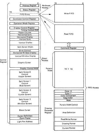
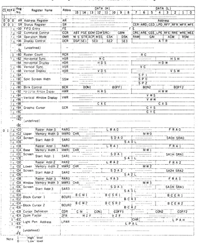
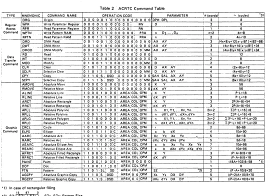
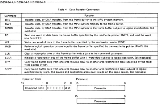
1 Registers of the ACRTC
---ELTEC-68K-SYSTEM
Documentation PIG1/68k
Revision A 5/86 Part C
Page
-2-The ACRTC occupies two wordwide VMEbus address locations,
which are documented in chapter 8.3.3 of this manual. The
ACRTC must be accessed as a wordwide device. In some cases
only the lowest 8 bits are siginificant, however.
In this chapter a short introduction is given to the ACRTC's
programming model. For more details you should read the
data sheet of the controller and other literature, which is published by Hitachi Ltd.
The ACRTC has over two hundred bytes of accessible
registers. These are organized as Hardware, Directly and
ELTEC Elektronik GmbH Mainz
1.1 Hardware accessible registers
ELTEC-68K-SYSTEM
Documentation PIG1/68k
Revision A 5/86 Part C
Page
-3-The lower address location of the ACRTC provides the status
register, when a read-cycle is performed. The status
register summarizes the ACRTC state and is used by the CPU
to monitor the overall operation of the ACRTC. When a
write-cycle is performed to the lower address-location, the address register is activated, in order to program the ACRTC with the address of the desired directly accessible internal register.
ELTEC Elektronik GmbH Mainz
1.2 Directly accessible registers
ELTEC-68K-SYSTEM
Documentation PIG1/68k
Revision A 5/86 Part C
Page
-4-These registers are accessed by prior loading of the address
register with the chosen register address. When the CPU
accesses the higher VMEbus-address location, the chosen register is activated.
The FIFO entry enables access to FIFO accessible registers using the ACRTC's read and write FIFO's.
The Command Control Register CCR is used to control overall ACRTC operation such as aborting or pausing commands,
defining DMA protocols, enabling/disabling interrupt sources etc.
The Operation Mode Register OMR defines basic parameters of ACRTC operation such as frame buffer access mode, display or drawing priority, cursor and display timing skew factors, raster scan mode etc.
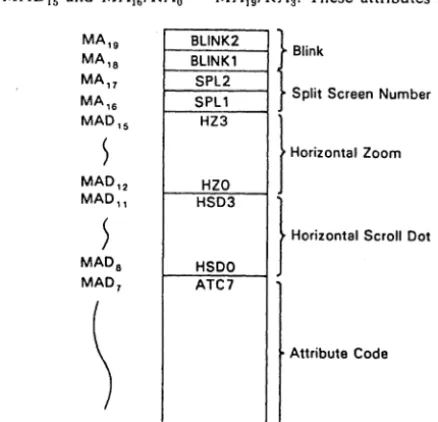
The Display Control Register OCR allows the independent enabling and diabling of each of the four ACRTC logical
display screens (Base, Upper, Lower and Window). Also this
register contains 8 bits of user defineab1e video attributes, the Attribute Register ATR.
The Timing Control RAM TCR contains registers which define
ACRTC video timing. This includes timing specification
registers for CRT control signals, logical display screen
size and display period, blink timing and so on. The names
of some important registers are:
- Horizontal Sync Register HSR - Horizontal Display Register HDR - Vertical Sync Register VSR
ELTEC Elektronik GmbH Mainz ELTEC-68K-SVSTEM
Documentat i'on PIG1/68k
Revision A 5/86 Part C
Page
-5-The Display Control RAM OCR contains registers which define logical screen display parameters such as start addresses,
raster addresses and memory width. Also included are the
cursor(s) definition, zoom factor and light pen registers. The names of some important registers are:
- Memory Width Registers MWR0 .•• MWR3 - Start AddressRegisters SAR0 ••• SAR3
ELTEC Elektronik GmbH Mainz
1.3 FIFO accessible registers
ELTEC-68K-SYSTEM
Documentation PIG1/68k
Revision A 5/86 Part C
Page
-6-For high performance drawing, key drawing processor
registers are coupled to the CPU via the ACRTC's separate 16-byte read and write FIFO's.
ACRTC commands are sent from the CPU via the write-FIFO to
the command register. As the ACRTC completes command
execution, the next command is automatically fetched from the FIFO into the command register.
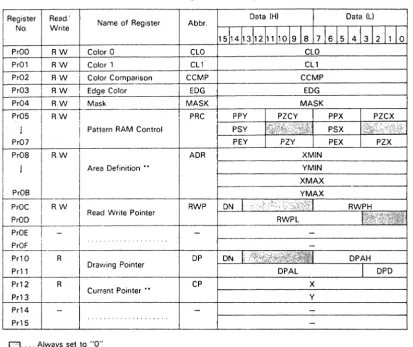
The pattern RAM is used to define drawing and painting
patterns. The pattern RAM is accessed using the ACRTC's
Read Pattern RAM (RPTN) and Write Pattern RAM (WPTN) register access commands.
The Drawing Parameter Registers DPR define detailed
parameters of the drawing process, such as color control,
area control and pattern RAM pointers. The DPR's are
acess~d using the ACRTC's Read Parameter Register (RPR) and
ELTEC E1ektronik GmbH Mainz
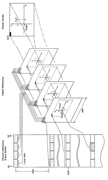
2 Frame-buffer interface of the ACRTC
---2.1 Introduction
ELTEC-68K-SYSTEM
Documentation PIG1/68k
Revision A 5/86
Part C Page
-7-The ACRTC has a 16-bit wide data interface to the frame
buffer lines (MAD0~ •• MAD15). These 16 bits can be defined
to be from 16 pixel in one plane to 16 planes of one pixel. On PIG1/68k all even MAO-lines are connected to the
data-port of the frame buffer. All odd lines are used for
the frame-buffer extension in the PIG2/68k-upgrade.
On PIG1/68k the frame buffer size is one MegaByte, which can be configured as one bitp1ane with eight MegaPixe1, as two planes with four MegaPixe1s each or as four planes with two
MegaPixe1s each. Please refer to part B of this manual for
correct adaption, concerning the hardware-videa-port.
According to the video-read-out configuration the ACRTC must
be programmed with the correct Graphic Bit Mode GBM. It is
important to have in mind, that the complete hardware is
designed for generating 8 bitp1anes with one ACRTC. If you
use PIG1/68k alone, the effective GBM must be twice the desired number of bitp1anes.
One of the design goals of PIG1/68k was to support the high drawing speed of the ACRTC by a suitable frame buffer
architecture. Modern video RAM-chips have been used to reduce the need of time for display refresh to an absolute minimum: Only one cycle per raster scan line is necessary
for that task. It is sufficient to program the ACRTC with a
horizontal display width of one, to load 4096 bits (physical
pixels) in the RAM's on-chip shift registers. In the
four-bitplane-mode 1024 logical pixels are provided for one
raster scan line, which is the maximum in that mode. In the
two-bitp1ane-mode 2048 logical pixels are provided and in
the one-bitp1ane~mode 4096 pixels per raster scan line are
ELTEC Elektronik GmbH Mainz ELTEC-68K-SYSTEM
Documentation PIG1/68k
Revision A 5/86 Part C
Page
-8-The dual-port-RAM architecture brings a very high throughput (factor 4 to 6 in comparison to conventional
frame-buffer-concepts), but there are some restrictions, which should be mentioned here:
- The window (fourth screen) has always the same width as the other screens - The horizontal pan feature (crawl) works
always within one module of logical pixels - The horizontal memory width must always
be defined modulo the number of logical pixels - The horizontal memory width has to be a power
of two (512, 1024, 2048 •• )
Some of these restrictions can be compensated by using the
powerful instruction set of the ACRTC efficiently. The
ELTEC E1ektronik GmbH Mainz
2.2 Colors and Bitp1anes
ELTEC-68K-SYSTEM
Documentation PIG1/68k
Revision A 5/86 Part C
Page
-9-Controlling of the color mode is done with the Drawing
Parameter Registers and wit~in that set especially with the
color registers COL0 and CaLl. Please notice, that always
all bits must be set according to the desired color. Please
refer to table C.2.1 for details!
Tab C.2.1: Color control for PIG1/68k
Color
BLACK GREEN RED BLUE SCRATCH YELLOW CYAN MAGENTA WHITE
Note:
Control Byte
$001 $01 $04-$lel $4el $0:1 $11 $14-$1:1
Register-value
GBM=3 GBM=2 GBM=l
$0000 $0000 $0000
$0101 $1111 $5555
$0404 $4444
$1010 $4040
$0505 $5555
$1111 $1414 $1515
Color ••••• means the effect on the monitor when
connected as described in chapter B! Register-va1ue ••• means the effective value to be
ELTEC Elektronik GmbH Mainz
3 Examples to set up the ACRTC
---ELTEC-68K-SVSTEM
Documentation PIG1/68k
Revision A 5/86 Part C
Page
-10-In table C.3.1 you will find some set-up's for different
monitors. It is important to have in mind, that the
horizontal CRT sync timing is given in units of memory
cycles. The length of one cycle is the dotrate, divided by
32. The length of the vertical parameters are given in
units of raster scan lines. Please notice, like mentioned
in the ACRTC data sheet, that some of the parameters must be subtracted by one before written into the ACRTC' registers. Table C.3.1 shows adjusted parameters.
Please note some general hints:
- The Grafic Address Increment parameter GAl should always be set to 2.
- The board should always be initialized as slave, even in standalone mode.
- The grafic bit mode GBM must always be twice the effective number of bitplanes,
if no frame-buffer extension is used.
- The display start addresses must be adjusted by several so-called kluge-factors, which must be subtracted from the desired display
start addresses. These factors depend on the
ACRTC's mask-version and therefore can change. The given examples are evaluated with as-mask. - The horizontal display width HOW should
always be set to one. The lrue parameter
ELTEC Elektronik GmbH Mainz ELTEC-68K-SVSTEM
Documentat i'on PIG1/68k
Revision A 5/86 Part C
Page
-11-Tab C.3.1: Set-up-examples for PIG1/68k (4 bitplane-mode)
Parameter Notes in ()
Hor Sync Width Hal" Cycle (1 ;2)
( 1 ; 2)
Hor Disp Width (1 ;2;4)
Eff Hor DislP Width (1 ;5)
Hal" Disp St.art ( 1 ; 2) Ver Sync Width (1; 2)
Ver Cycle (1 ;2)
Ver Disp Width (1; 2) Vel" Disp Start (1; 2) Hor Plane Width ( 1 ; 2) Graphic Bit Mode (1; 2) GAl Mode ( 1 ; 2)
Operation Mode (1 ; 3)
Kluge Factor: (2;6) Screen 13 (Upper) Screen 1 (l8ase) Screen 2 (Lower) Screen 3 (Window) Dotclock (7)
Horiz. frequency in kHz
Field frequency (8)
Notes:
Monitor-Type 0 1 2
2 2 3
27 45 41
1 1 1
19 31 31
2 6 3
3 3 113
625 625 8513
512 512 785
67 67 40
4096 1024 11324
3 3 3
2 2 2
41eB 41138 41138
4 4 4
13 4 4
4 4 4
13 13 13
14 48 55
15.6 32.13 42.13
50 513 513
1 ••• Parameter given not ~egister-value
2 ••• Decimal notation 3 ••• Hexadecimal notat ion
4 ••• 0nly one cycle because of Dual-part-RAM 5 ••• Please refer to chapter C.4
Name ACRTC
Reg
HSW HSR
HC HSR
HOW HDR
ATR
HDS HDR
VSW VDR
VC VSR
SPx SSW
VDS VDR
MW MWR
GBM CCR
GAl OMR
OMR
SARe SAR1 SAR2 SAR3
6 ••• To be subtracted from desired display start address 7 ••• The dotclock is given in MHz with U6el
ELTEC Elektronik GmbH Mainz
4 The Horizontal Display Width
---ELTEC-68K-SYSTEM
Documentation PIG1/68k
Revision A 5/86 Part C
Page
-12-As mentioned earlier. the effective horizontal display width
(HOW) is programmed with register ATR. To be compatible
with the ACRTC's normal nomenclature. it is recommended to calculate this parameter like to be written into register HDR.
Example:
If you want to have a horizontal
display width of 1024 pixels on the screen with the four-bitplane-mode (GBM=3)
the equivalent parameter HOW is 31 (32 minus 1).
The lower byte of register HDR should be set to one and the effective horizontal display width must be transformed in the following way:
First step: Complement HOW
Second step: Apply AND-mask of hex 3E
ELTEC Elektronik GmbH Mainz
5 Crawl
---ELTEC-68K-SYSTEM
Documentation PIG1/68k
Revision A 5/86 Part C
Page
-13-Crawling is defined as repositioning the screen on the
display memory in horizontal direction. In general always
ACRTC·s registers SARx are used for panning. If you want to
use the horizontal pixel-by-pixel pan-feature the parameter Start Dot Address SDA within the SAR-registers are used. Those four bits define the offset of the screen position within that module which can be reached with the used grafic
bit mode G8M. Please refer to table C.5.1!
Tab C.5.1: Significance of SAR-bits
G8M SAR-bits
3 2 1
Note:
011 010 009 008
x x
x
x x 4
x
2 2
1 1 1
G8M ••••• means grafic bit mode, which corresponds to the hardware-adapted number of bitplanes x ••••••• not used - should be set to zero
ELTEC Elektronik GmbH Mainl
6 Zoom
ELTEC-68K-SYSTEM
Documentation PIG1/68k
Revision A 5/86 Part C
Page
-14-Programming the zoom-factor is very easy. The ACRTC has a
special Zoom Factor Register ZFR. Four bits are used for
the horizontal and another four bits are used for the
vertical zoom factor VZF. The vertical zoom factor is used
only within the ACRTC to modify vertical display refresh
addressing. All 16 factors can be used. The horizontal
zoom factor HZF is used by the ACRTC and external hardware,
which supports only factors of 1,2 and 4. That is why only
these factors should be used for horizontal zooming. Please
refer to table C.6.1!
Tab C.6.1: Allowed horizontal zoom factors
Zoom factor
1 2 4
Note:
ZFR-Bits for HZF
015 014 013 012
o
o
o
o
o
o
o
o
1
o
1 1
ZFR •••• means Zoom Factor Register HZF •••• means Horizontal Zoom Factor
ELTEC Elektronik GmbH Mainz
7 Blinking
---ELTEC-68K-SYSTEM
Documentation PIG1/68k
Revision A 5/86 Part C
Page
-15-Blinking is controlled via shapes generated in the scratch
bitplane. Blinking must be hardware-enabled with Jumper
J1003 as described in part B of this manual. With ACRTC's
register BCR <Blink Control Register) the blinking rate can
be modified and software-enabled/disabled. Only the
ELTEC Elektronik GmbH Mainz
8 Hardware status register
---ELTEC-68K-SYSTEM
Documentation PIG1/68k
Revision A 5/86 Part C
Page
-16-The hardware status register is an extra byte-wide register.
It can be read and written. For address and bus-cycle
please refer to chapter B.3!
It is intended to be used normally as ID/vector-register for
the VMEbus interrupt-acknowledge cycle. But it can also be
used for establishing semaphores and so on.
ELTEC Elektronik GmbH
00.68 01749
E L T E C 6 8 K - S Y S T E M
DOCUMENTATION
PIG1/68k
ELTEC Elektronik GmbH Mainz
Preface
---ELTEC-68K-SYSTEM
Documentation PIG1/68k
Revision A 5/86 Part D
Page
-2-This part of the documentation is dedicated to all users, who want to deal with the hardware in detail, as in field service, for instance.
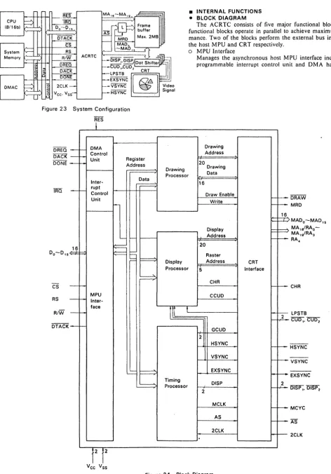
The hardware is designed modular. The several blocks are:
- VMEbus interface
--) wiring diagram 1
- Control logic for VMEbus and local bus --) wiring diagram 2
- Status/vector register --) wiring diagram 3
- Advanced Cathode Ray Tube Controller ACRTe --) wiring diagram 4
- Frame-buffer interface --) wiring diagram 5 - Central timing logic
--) wiring diagram 6
- Two-port-RAM timing generator --) wiring diagram 7
- Video shift-register --) wiring diagram 8 - Frame-buffer
--) wiring diagram 9 - Monitor interface
ELTEC Elektronik GmbH Mainz
1 VMEbus interface
-Circuit diagram 1 shows the VMEbus interface.
ELTEC-68K-SYSTEM
Oocumentatfon PIG1/68k
Revision A 5/86 Part 0
Page
-3-The data bus is coupled via transceivers U101 and U102. The
internal data bus is called 1000 to 1015. U103 and U104
generate the line /BAOO (base address decoder out), if the base address and the appropriate address modifiers are decoded.
All internal IJMEbus 1 ines have the prefix "1" to show that they are of the same function, but internal.
ELTEC Elektronik GmbH Mainz
2 Control logic for VMEbus and local bus
---ELTEC-68K-SVSTEM
Documentation PIG1/68k
Revision A 5/86 Part 0
Page
-4-U201 latches all control lines, which are necessary for
internal use. U202 buffers control lines /DS0 and
/SVSRESET. Circuit diagram 2 shows details of this module.
PAL U204 decodes the devices and handles the VMEbus logic,
including the VMEbus interrupt control logic. U203 decodes
a valid interrupt acknowledge cycle (line /VIACKCV). U202
buffers the internal IRQ-line. With jumper J201 the desired
interrupt level and the appropriate acknowledge level are selected.
All bus grant lines are connected in the printed circuit layout, so there is no need to jumper them on the backplane.
ELTEC Elektronik GmbH Mainz
3 Status/vector register
---ELTEC-68K-SYSTEM
Documentatinn PIG1/68k
Revision A 5/86 Part D
Page
-5-Circuit diagram 3 shows the status/vector register.
U301 is a 8 bit wide register, called PIG.STAT. The
register can be programmed to contain the interrupt vector. Otherwise it can be used as a general purpose register to store semaphores etc.
4 Advanced Cathode Ray Tube Controller (ACRTC)
---Circuit diagram 4 shows the ACRTC-module.
U401 is the central device of the board. It is decoded by
the line /ENACRTC. NAND-gate U402 is used for external
synchronisation of the board.
ELTEC Elektronik GmbH Mainz
5 Frame-buffer interface
---ELTEC-68K-SYSTEM
Documentation PIG1/68k
Revision A 5/86 Part D
Page
-6-Circuit diagram 5 shows details of this module.
U501 is a buffer, which connects the multiplexed
data/address-bus of the ACRTC with the databus of the
frame-buffer. U502 is a registered multiplexer to address
the frame-buffer. U503 and U504 are used to store some of
the ACRTC's attribute-bits and the video-address-lines
VA17-VA19. These lines are used to select the different
RAM-banks. U505 stores the least significant
video-address-line VA0, which must be done, because of the ACRTC's multiplexed memory bus.
ElTEC Elektronik GmbH Mainz
6 Central timing logic
---ElTEC-68K-SYSTEM
Documentation PIG1/68k
Revision A S/86 Part 0
Page
-7-Circuit diagram 6 shows details of this module.
U601 is the central dot clock oscillator, which can/must be
adapted to the desired monitor parameter set. Jumper J601
defines whether the dotclock comes from the on-board
oscillator or from another PIG-board. U606 is clocked by
the dotclock to generate other timing control lines. U608
buffers these lines to get a defined and stable timing
relationship. The line 2ClK clocks the ACRTC and line ClK8
is used to control the RAM-timing. J602 and J603 must be
set properly according to the desired bitp1ane mode.
U607 and U609 have nearly the same function as U606 and U608, but are clocked via a selectable frequency to control the horizontal video zoom capability.
U604 and U60S form a display-enable-signal, which is
independent of the ACRTC. This must be done, because the
ACRTC does not support the modern two-port-video-RAM's
properly. The desired horizontal display width must be
programmed with attribute lines MAD1 to MADS. The ACRTC's
horizontal width parameter determines only, how often a video refresh cycle will be done per raster scan line. Normally one video refresh cycle is necessary.
ELTEC Elektronik GmbH Mainz
7 Two-port-RAM timing generator
---ELTEC-68K-SYSTEM
Documentation PIG1/68k
Revision A 5/86 Part 0
Page
-8-Circuit diagram 7 shows details of this module.
Shift register U702 generates basic timing signals, which are used in PAL U701 to form the RAM-control-lines.
8 Video shift-registers
---For details see circuit diagram 8!
U802 and U803 store a group of 16 pixels, which are read out
of the frame buffer at a time. Counter U801 generates
several load-pulses for the shift registers. The chip is
programmed with lines ATTSCx, which are the ACRTC's start
dot address. With this circuitry it is possible to program
the phase relationship between the line RAMCK, which serve as a clock to buffer the video data and the lines LDHI and LDLO, which load two shift register modules.
The first set of shift registers U806 to U809 is clocked by
line CLKLO. The pixel-rate is multiplied by four in this
stage. The next stage is built by shift register U810,
which has different functions: In the four-bitplane-mode it serves only as a register; in other modes it increases the
pixel-rate once more. It is important to notice, that
ELTEC Elektronik GmbH Mainz
9 Frame-buffer
---For details see circuit diagram 9!
ELTEC-68K-SYSTEM
Documentation PIG1/68k
Revision A 5/86
Part D Page
-9-U906 to U937 are dual-port-video-RAM·s, containing the
bitmap, generated by the ACRTC. U901 buffers the
multiplexed RAM-address-lines. The RAM-chips are organized
to 8 banks of 4 chips each. U902 controls the serial port
of the several banks. U903 and U904 activate two out of 16
different IRASxx-lines to select two RAM-chips at a time for
the ACRTC's random access to the frame-buffer. On PIGl/68k
all odd lines of the ACRTC's memory port are connected to the frame-buffer, having all even lines reserved for the eight bit version of the board PIG2/68k.
ELTEC Elektronik GmbH Mainz
10 Monitor interface
=================
For details see circuit diagram 10!
ELTEC-68K-SYSTEM
Documentation PIG1/68k
Revision A 5/86 Part 0
Page
-10-Video-lines SOx are 'ANDed' with the synchronized display
enable signal DISPEN, which is available at connector X10 as
MBLK and at connector Xll for the local display memory
extension. The video-lines are clocked the first time and
then ANDed with the blink-enable line BLINKEN. After the
second register stage they are driven with buffer U602 and connected to the resistor-network for optional greyscale operation.
The mpnitor sync signals are synchronized with U1005. With
ELTEC Eleklronik GmbH
00.68 01749
E L T E C 6 8 K - S Y S T E M
DOCUMENTATION
PIG1/68k
ELTEC Elektronik GmbH Mainz ELTEC-68K-SYSTEM
Documentation PIG1/68k
Revision A 5/86 Appendix
Page
-2-Appendix A: Address modifier VMEbus
hex Addres·:, modifier
Code 5 4 3 2 1 0 Access Note
---3F H H H H H H Standard Supervisory Ascending 1
3E H H H H H L Standard Supervisory Program 1
3D H H H H L H Standard Supervisory Data 1
3C H H H H L L Undefined 2
38 H H H L H H Standard Non-Privileged Ascend 1
3A H H H L H L Standard Non-Provileged Program 1
39 H H H L L H Standard Non-Privileged Data 1
38 H H H L L L Undefined 2
30-37 H H L x x x Undefined 2
2F H L H H H H Undefined 2
2E H L H H H L Undefined 2
20 H L H H L H Short Supervisory I/O 1
2C H L H H L L Undefined 2
28 H L H L H H Undefined 2
2A H L H L H L Undefined 2
29 H L H L L H Short Non-Privileged I/O 1
28 H L H L L L Undefined 2
20-27 H L L x x x Undefined 2
10-1F L H x x x x Undefined 3
0F L L H H H H Extended Supervisory Ascending 1
0E L L H H H L Extended Supervisory Program 1
00 L L H H L H Extended Supervisory Data 1
0C L L H H L L Undefined 2
08 L L H L.H H Extended Non-Privileged Ascend 1
0A L L H L H L Extended Non-Privileged Program 1
09 L L H L L. H Extended Non-Privileged Data 1
08 L L H L L L Undefined 2
00-07 L L L )( x x Undefined 2
Notes:
1 •••• Defined by VMEbus Specification 2 •••• Definition reserved
ELTEC Elektrorik GmbH Mainz
Appendix B: Jumpers, switches
Id No
S101 S102 S103 J101 J201 J202 J203 J401 J501 J601 J602 J603 J604 J801 J802 J803 J804 J1001 J1002 J1003 Funct ion
VMEbus base address VMEbus base address VMEbus address modifier Decoding of AM2
VMEbus interrupt level External access
External access
Master/slave-operation Operation of PIG2-config Master/slave-operation Selects no of bitplanes Selects no of bitplanes Master/slave-operation Selects no of bltplanes Selects no of bitplanes Selects no of bitplanes Selects no of bitplanes Jumper for V-sync
Jumper for H-sync Enables blinking
ELTEC-68K-SVSTEM
Documentation PIG1/68k
Revision A 5/86 Appendix
Page
-3-Refer to chapter
B.3.1; 0.1 B.3.1; 0.1 B.3.2; 0.1 B.3.2; 0.1 B.3.4; 0.2
B.7; 0.2
B.7; 0.2
ELTEC Elektronlk GmbH Mainz
Appendix C: Connectors
ld No Function
Xl VMEbus-connector Pl
X2 not used
X3 H-sync output
X4 V-sync output
X5 Green output
X6 Red output
X7 Blue output
X8 Scratch output
X9 Dotclock output/input
X10 Blanking output
Xll Local frame buffer' bus
X12 Local bus
X13 External synchronisation
X14 Prescaler reset
ELTEC-68K-SYSTEM
Documentation PIG1/68k
Revision A 5/86 Appendix
Page
-4-Type
96-pin DIN4l6l2
Mini BNC Mini BNC Mini BNC Mini BNC Mini BNC Mini BNC Mini BNC Mini BNC
64-pin DIN4l6l2 2*25 pin female Mini BNC
ELTEC Elektronik GmtH Mainz ELTEC-68K-SYSTEM
Connector Xl (VMEbus)
Signals in brackets have
Pin No Row A
Documentation PlG1/68k
Revision A 5/86
Appendix Page
-5-no connection to the board.
Row B Row C
- - - ----_ ...
_---1 000 (/BBSY) 008
2 001 (lBCLR) 009
3 002 (lACFAlL) 010
4 003 IBG0lN 011
5 004 IBG00UT 012
6 005 IBG1lN 013
7 006 IBG10UT 014
8 007 IBG2lN 015
9 GNo IBG20UT GNo
10 (SYSCLK) IBG3lN (/SYSFAlL)
11 GNo IBG30UT IBERR
12 (loSl ) (lBR0) ISYSRESET
13 IOS0 (lBR1> ILWORo
14 IWRlTE (/BR2) AM5
15 GNo (lBR3) (A23)
16 10TACK AM0 (A22)
17 GNo AMI (A21)
18 (lAS) AM2 (A20)
19 GNo AM3 (A19)
20 IlACK GNo (A18)
21 IlACKlN (SERCLK) (A17)
22 IlACKOUT (SERoAT) (A16)
23 AM4 GNo A15
24 A07 IIRQ7 A14
25 A06 IIRQ6 A13
26 A05 IlRQ5 A12
27 A04 IIRQ4 All
28 A03 IlRQ3 A10
29 A02 IIRQ2 A09
30 A01 IIRQl A08
31 (-12V) (+5VSToBY) (+12V)
ELTEC Elektronik GmbH Mainz
Connector Xll
ELTEC-68K-SYSTEM
Documentation PIG1/68k
Revision A 5/86
Appendix Page
-6-This connector is used for PIG2/68k-configuration.
Pin No Row A Row B Row C
---1 DOTCLKPll +5V GND
2 GND GND MAe
3 MAl MA2
4 MA3 MA4
5 MAS GND
6 MA7 GND
7 VA18 -12V
8 VA19 +5V
9 VA0 +12V
10 RAMCK
11 IOERAM IOEBUF
12 IWERAM GND MRD
13 CLKLO +5V
14 IRASl
15 . LDHI
16 RASPOL
17 ICAS
18 IHSYNC
19 LDLO
20 DISPEN
21 BLINKEN
22 MADl GND
23 MAD3
24 MADS
25 MAD7
26 MAD9
27 MAD11
28 MAD13
29 MAD15 MAD18
30 MAD17 +5V
31 MAD19 GND MA6
ELTEC E1ektronik GmbH Mainz
Connector X12
This connector is dedicated for
bus. Lines in () are not used.
external
ELTEC-68K-SYSTEM
Documentation PIG1/68k
Revision A 5/86
Append i x Page
-7-access to 1 oca 1
Pin No Pin No
odd Signal even Signal
---1 reserved 2 reserved
3 HCTRL0 4 IGOCOONE
5 /GOCOREQ 6 IGOCOACK
7 /IOS0 8 IIWRITE
9 /IRES 10 ( j 10Sl)
11 (SYSCLK) 12 (A19)
13 (A18) 14 (A17)
15 (A16) 16 (A15)
17 (IA14) 18 (IA13)
19 (lA12) 20 ( IAll)
21 (IA10) 22 (IA09)
23 (IA08) 24 <IA07)
25 (IA06) 26 (IA05)
27 IA04 28 IA03
29 IA02 30 IA01
31 /OBEN 32 IBAOO
33 /ERR 34 IROY
35 1.015 36 1014
37 1.013 38 1012
39 1.011 40 1010
41 1.009 42 1008
43 1.007 44 1006
45 1.005 46 1004
47 1.003 48 1002
ELTEC Elektronik GmbH Mainz
Appendix D: Sample program
ELTEC-68K-SYSTEM
Documentation PIG1/68k
Revision A 5/86 Appendix
Page
-8-"''''''''''''''''''''''''''''''' "''''''' "'''' "''''''''''''' "'''' "''''''' -8-"'''''''''''''''''''''''''''''''''''''''''''''''''''' "''''''''''''''''''' "'*'" "'**"'*"''''''''''''''''*''''''''''''*'''*''''''
'" Demonstration for PIG1 / HD 63484 '"
'"
'" This program shows the initialization of the ACTRC and draws '" on the screen one rectangle and some lines
'"
'" (C) Eltec Elektronik GmbH Mainz
'"
'" rb 220586'"
'"
*
'"
'"
'"
'"
"''''''''''* *"''''''''''''''''''''''''' "'''' "'''''''''''''''''''*'''''' "''''*''' * "'''''''''''''*'''*''''''''''''''''''*'''''''''*''''''* *"''''*'''*'''*''''''***'''**''''''''''''''''" OS9-specific declarations use <oskdefs.d>
S t k e q u 100 '" some de f a u 1 t stack size psect pigdemo, (Prgrm«8) !Objct, (ReEnt«8)! 1,0,Stk,pigdemo
'" end of OS9-specific declarations acrtc equ
memtot equ GBM equ
'"
ON equ
linpix equ memwid equ
'" linnum equ
startad equ
'"
drawpoi equ
'"
GAl'"
OMR'"
OCR'"
equ equ equ $ff8d00 $100000 3 1«30 10241 in pix» (4-GBM) memtot/memwid memtot-(785"'memwid)-4 DN+«memtot-memwid>«4) 2 $4108+(GAI«4) $4020
*
Hardware Adress of Master Status '" Total memory is 1 megawords*
log (2) of Bit/pixel for PIG2; this can be 1, 2 or 3.'" Base screen is specified
* Pixel/line
'" 512 Words/line (16 bit; 8 bit with PIG!)
'" total number of 1 ines '" Start Address (upper left)
4 is 'Kluge factor'
'" Drawing Pointer for (0,0) on Base Screen
Operation Mode Register OMR '" Start, Slave, GAI=2,Dual Access
Display Control Register OCR '" Enable Base Screen;
ELTtC Elektronik GmbH Mainz ELTEC-68K-SYSTEM
Documentation PIG1/68k
Revision A 5/86 Appendix
Page
-9-***************.****************************************************
*
*
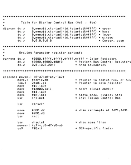
Table for Display Control Ram <$ce •. $de)*
dispcon dc.w e,memwid,startad»16,<startad&$ffff) 0,memwid,startad»16,<startad&$ffff) 0,memwid,startad»16,<startad&$ffff) 0,memwid,startad»16,(startad&$ffff) 0,13,13,13,13,13
* upper dc.w
dc.w dc.w dc.w
* base
* 1 ower
* window
* Cursor, zoom
*********~**********************************************************
*
*
Drawing Parameter register contents*
parreg: dc.w $eeee,$ffff,$ffff,$ffff,$ffff
*
Color Registers dc.wdc.w 13,13,11323,21347 $eeee,$eeee,$eefe
*
* Area boundaries Pattern Ram Control Registers ******************************************************************** pigdemo: movem.l de-d7/ae-a6,-<a7)move.l #acrtc,ae 1 ea.l 2(ae) ,al move #$2,<ae) move #$8131313, <a1) move #$4, <ae) move #$e,<al) bsr intimct
bsr clrscrn
move move bsr
bsr movem. I os9 #3e0,d2 #2ee,d3 rect drawtst (a7)+,de-d7/ae-a6 F$Exit
* Pointer to status reg. of ACRTC
*
Pointer to data register*
Abort (Reset ACRTC)*
slave mode, display stop*
lnit Timing Control Ram*
draw rectangle at <d2>,<d3>*
draw some lines [image:78.615.91.511.184.712.2]ELTEC Elektronik GmbH Mainz
*
* set RW POINTER to lower 1 eft *
setrwp: move #$080c,dl bsr wr fifo move.l #drawpoi,dl swap dl
bsr wrfifo move #$080d,dl bsr wrfifo swap dl bsr wrf ifo rts
*
* Move graphics cursor to x=<d2); *
amove: move #$8000,dl bsr wrfifo move d2,dl bsr wrfifo move d3,dl bsr wrfifo rts
*
*
write one byte into the fifo*
wrfifo: move wrfifl: move and beq.s move rts
#0, (a0) (a0),d6 #2,d6 wrfifl dl,(al)
ELTEC-68K-SYSTEM
Documentation PIGl/68k
Revision A 5/86
Appendix Page
-10-* Write Pattern Ram
* write lower half register
*
upper halfy=<d3)
* AMOVE command
* X
* Y
*
status register is addressed* read status register
*
Write fifo ready?* Wait for it