Electrochemically Deposited Ceria Structures for
Advanced Solid Oxide Fuel Cells
Thesis by
Evan C. Brown
In Partial Fulfillment of the Requirements For the Degree of
Doctor of Philosophy
California Institute of Technology Pasadena, California
2011
Acknowledgements
Foremost, I would like to dedicate this work to the One who loved me first. Truly, there is no greater love than one who lays down his life for another.
I would like to thank my wife for giving me such support and encouragement. Those words are easily written, but they were never given lightly by her. As for the rest of my family, I would not have accomplished much without all of their love and their crazy; especially my parents, who inspire me and have always reminded me who I am.
Abstract
As the pursuit towards emissions reduction intensifies with growing interest and nascent technologies, solid oxide fuel cells (SOFCs) remain an illustrious candidate for achieving our goals. Despite myriad advantages, SOFCs are still too costly for widespread
deployment, even as unprecedented materials developments have recently emerged. This suggests that, in addition to informed materials selection, the necessary power output— and, thereby, cost-savings—gains must come from the fuel cell architecture. The work presented in this manuscript primarily investigates cathodic electrochemical deposition (CELD) as a scalable micro-/nanoscale fabrication tool for engineering ceria-based components in a SOFC assembly. Also, polymer sphere lithography was utilized to deposit fully connected, yet fully porous anti-dot metal films on yttira-stabilized zirconia (YSZ) with specific and knowable geometries, useful for mechanistic studies. Particular attention was given to anode structures, for which anti-dot metal films on YSZ served as composite substrates for subsequent CELD of doped ceria. By tuning the applied
potential, a wide range of microstructures from high surface area coatings to planar, thin films was possible. In addition, definitive deposition was shown to occur on the
Table of Contents
Acknowledgements………..……… iii
Abstract……… iv
Table of Contents………. v
List of Figures……….. x
List of Tables……… xvi
List of Symbols and Notations……… xviii
1 Introduction and Background………. 1
1.1A Global Perspective………... 1
1.2SOFC Introduction……….. 3
1.2.1 SOFC Basics………. 3
1.2.2 Materials Selection: Samaria-Doped Ceria (SDC) ………... 7
1.2.3 Cell Architecture………... 10
1.3Anti-Dot Substrates: A New Design Framework……… 12
1.4Three-Dimensional Structures and Their Fabrication by CELD………. 14
1.4.1 SOFC Fabrication Method/Morphology Non-Negotiables…………..…. 14
1.4.2 Cathodic Electrochemical Deposition (CELD)………. 16
2.1Polymer Sphere Lithography Background and Summary………... 19
2.2Experimental Details……… 23
2.2.1 Substrate Preparation………. 23
2.2.2 Nanosphere Deposition………. 23
2.2.3 Microsphere Deposition……… 23
2.2.4 Metal Deposition………... 24
2.2.5 Microstructure Analysis……… 24
2.2.6 High Temperature Stability………... 25
2.3Results and Discussion……… 25
2.3.1 Nanosphere Lithography Results……….. 25
2.3.2 Microsphere Lithography Results………. 26
2.3.3 Microstructure Fidelity……….. 31
2.3.4 Thermal Stability………... 36
3 Cathodic Electrochemical Deposition of Undoped and Doped Ceria……….. 38
3.1Introduction……….………… 38
3.2Experimental Details……… 40
3.2.1 Substrate Definition………... 40
3.2.2 Experimental Setup………... 42
3.2.3 Characterization Details……… 45
3.3Results………. 46
3.3.1 Bulk………... 46
3.3.2 High Surface Area (HSA) Coatings……….. 52
3.4Discussion……… 64
3.4.1 General Deposition Overview………... 64
3.4.2 The Physical Deposition Picture………... 69
3.4.3 Deposition on Non-Conducting Parts of the Substrate………. 71
3.4.4 HSA and Thin Film Transients………. 79
4 The Electrochemical Activity of CELD Ceria Structures………. 84
4.1Introduction, Methods, and Background………... 84
4.1.1 A.C. Impedance Spectroscopy (ACIS) Introduction………. 84
4.1.2 Experimental Approach………. 87
4.1.3 System Precedence……… 90
4.2Arc Identification: PLD Films vs. CELD Coatings………... 91
4.2.1 Representative Spectra……….……… 91
4.2.2 Origin of the Single Arc in the Metal-Sandwich Configuration….……. 94
4.2.3 Origin of the HF Arc in Embedded Metal Configurations….………….. 97
4.2.4 Origin of the LF Arc in Embedded Metal Configurations..………. 102
4.3The SDC|Gas Interface Arc: A Closer Look………..………... 104
4.3.1 Platinum Strips……….. 104
4.3.2 Nickel Anti-Dot Films………... 115
5 Sundry Specialized CELD Microstructures………... 121
5.1Anodic Aluminum Oxide (AAO) Templated Nanowires……… 121
5.1.1 AAO Template Formation Mechanism and Background……….. 121
5.1.3 AAO Template Results………. 126
5.1.4 Ceria Nanowire Growth……… 133
5.2Inverse Opals………135
5.2.1 Inverse Opal Definition and Background……….. 135
5.2.2 Inverse Opal Fabrication Details………136
5.2.3 Inverse Opal Results……….. 136
5.3Oxidation Protection Coatings………. 138
5.3.1 Experimental Details………. 138
5.3.2 Results………... 139
5.4CELD Ceria Grown Directly on MIEC SOFC Cathode Substrates……… 140
5.4.1 Substrate Preparation Details……… 141
5.4.2 CELD Results and Discussion……….. 143
6 Summary and Conclusions……….. 150
Appendix A: ImageJ Analysis Details……… 152
Appendix B: Additional Images……….……… 155
B.1 Additional CELD Images……….………. 155
B.2 Additional AAO Images……… ………158
B.3 Additional Inverse Opal Images……… 160
B.4 Additional MIEC Substrate Images……….. 160
B.5 Additional Oxidation Protection Coating Images………. 161
C.1 Solution Impregnation into AAO Templates………... 162 C.2 Copper Nanowire Synthesis……….. 165
List of Figures
1.1 SOFC schematic………..……….. 4
1.2 SOFC polarization curve………..………..6
1.3 Electrolyte materials’ ionic conductivity comparison…………..…………. 8
1.4 3PB and 2PB in powder-processed electrodes schematics……….…..……. 10
1.5 Anti-dot film and templated electrode microstructure schematics…..…….. 15
2.1 SEM images of the polymer sphere lithography process………..…… 20
2.2 Representative anti-dot film SEM images………..……….…….. 22
2.3 SEM images of nanosphere short- and long-range coverage……..………... 26
2.4 SEM images of nanosphere coverage for 500, 680, and 790 nm spheres... 27
2.5 SEM images of multilayers and void regions from microsphere
deposition... 28
2.6 Optical photographs of multilayers and void regions…………..………….. 28
2.7 Optical photographs of the water wash method………..……….. 30
2.8 Optical and SEM images of one spin coat with the water wash method…... 30
2.9 SEM images of microsphere coverage for 2 and 3.2µm spheres………..…. 31
2.10 Pore diameter histograms of Cu anti-dot films……….. 33
2.11 2PB area fraction histograms of Cu anti-dot films……… 33
2.12 SEM and AFM images of Ni anti-dot films before and after thermal
treatment……… 37
3.1 Pourbaix diagram for the Ce-H2O-H2O2 system from ref [86]………. 40
3.3 CELD setup schematic with corresponding potential electrode values…... 44
3.4 XRD and EDS analyses of undoped and doped bulk CELD ceria……..….. 47
3.5 Raman analyses of undoped and doped bulk CELD ceria…..………... 48
3.6 FT-IR analyses of undoped and doped bulk CELD ceria…………..……… 51
3.7 TGA analyses of undoped and doped bulk CELD ceria………..………….. 51
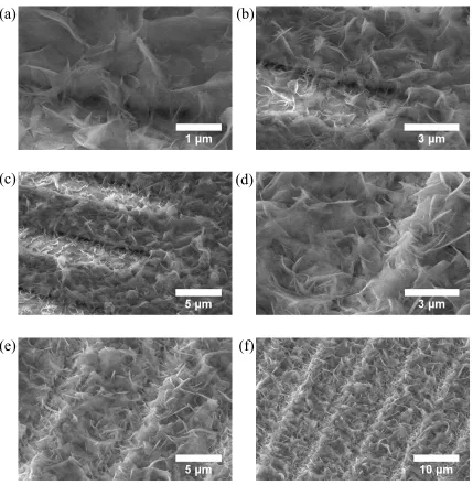
3.8 SEM images of undoped HSA ceria on YSZ/Pt strips…..……… 53
3.9 SEM images of doped HSA ceria on various substrates…..………. 54
3.10 SEM images of HSA ceria deposited from the doped + H2O2 electrolyte.... 55
3.11 SEM images of the HSA microstructure’s thermal stability………. 56
3.12 SEM images of a crack-free HSA structure after annealing……….. 57
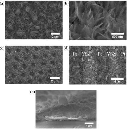
3.13 SEM images of as-deposited thin film morphologies……… 58
3.14 AFM scans of as-deposited thin films from the doped and doped + H2O2 electrolytes………. 59
3.15 SEM cross-sectional images of thin film morphologies……….... 60
3.16 SEM images of the deposits from the doped + acetic electrolyte………….. 62
3.17 SEM images showing the thermal stability of thin films on YSZ/Pt strips... 63
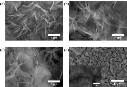
3.18 CV scan for the doped and doped + H2O2 electroltyes…….………. 68
3.19 SEM images of as-deposited HSA CELD ceria growth on exposed YSZ surfaces……….. 73
3.20 SEM images of as-deposited planar CELD ceria growth on exposed YSZ surfaces……….. 75
3.21 SEM images of equivalent HSA growth on YSZ and Pt strip regions….…. 76
YSZ/Pt strips substrate………. 78
3.23 TEM and HRTEM images of HSA CELD ceria………... 78
3.24 HSA voltage transients and corresponding chronological SEM images…... 80
3.25 Thin film current transients……… 82
4.1 Representative Nyquist plot for a PLD/Pt strips exposed configuration….. 85
4.2 Schematics showing 2PB reaction pathways for lithographically
defined substrates, metal-embedded and metal-sandwich configurations for
PLD and CELD samples for ACIS studies……….………... 89
4.3 SEM images of PLD and CELD metal-embedded samples…..……… 90
4.4 Representative Nyquist plots for PLD and CELD metal-embedded
samples……….…. 92
4.5 Nyquist plots with hydrogen and water partial pressure dependencies for a representative CELD/Ni anti-dot-embedded sample………. 93
4.6 Representative Nyquist plots for metal-sandwich configurations………… 94
4.7 Hydrogen partial pressure dependence of the single arc from metal-exposed and metal-sandwich configurations…………..………..…..………. 95
4.8 SEM images of the deleterious phenomena associated with CELD/metal-sandwich samples………...96
4.9 Hydrogen partial pressure dependence of the HF arc from metal-embedded configurations……… 98
4.11 TEM images showing voids in the HSA CELD deposit near the exposed
metal surfaces……….. 101
4.12 Hydrogen partial pressure dependence of the LF arc from metal-embedded and the single arc from metal-exposed configurations………. 103
4.13 Pt pattern size effect on the SDC|gas interfacial ASR partial pressure
dependencies………. 106
4.14 SEM images of undoped CELD ceria on 5-5 µm and 20-20 µm Pt patterns
on YSZ…………..……….... 106
4.15 Undoped CELD deposition time effect on the SDC|gas interfacial ASR
partial pressure dependencies………..………. 108
4.16 SEM images of undoped CELD ceria samples deposited for 5 and 10
minutes……….. 108
4.17 Doped CELD deposition time effect on the SDC|gas interfacial ASR partial pressure dependencies……….……….………. 109
4.18 SEM images of doped CELD ceria samples deposited for 5, 10, and 20
minutes………... 109
4.19 Doping effect for 5 minute deposits on the SDC|gas interfacial ASR partial pressure dependencies………..………...…….. 110
4.20 SEM images of doped and undoped CELD ceria samples deposited for 5 minutes………... 111
4.22 SEM images of doped and undoped CELD ceria samples deposited for 10
minutes………... 111
4.23 Consecutive depositions effect on the SDC|gas interfacial ASR partial pressure dependencies……….………. 113
4.24 SEM images of consecutive depositions following thermal treatment…... 114
4.25 SEM image comparison of doped CELD/Ni anti-dot-embedded samples deposited for 5, 10, and 20 minutes……….. 117
4.26 Deposition time effect for doped CELD/Ni anti-dot-embedded samples on the SDC|gas interfacial ASR partial pressure dependencies……….. 118
4.27 SEM image comparison of two doped CELD HSA samples and one doped CELD planar sample………. 119
4.28 SDC|gas interfacial ASR partial pressure dependencies comparison between two HSA and one planar doped CELD samples………. 120
5.1 AAO structure schematic………..………. 122
5.2 SEM images of AAO templates grown from Al foil……..………... 127
5.3 SEM image comparison of phosphoric acid pore diameter etching times... 128
5.4 SEM images of AAO templates grown from sputtered Al thin films…….... 129
5.5 Current transients for AAO templates grown from various Al thin film samples, whose optical photographs are also shown……… 130
and sputtered Al thin films………... 132
5.7 SEM images of as-deposited CELD ceria nanowires in the pores of AAO.. 134
5.8 SEM images of AAO ceria nanowires after thermal treatments…..……….. 134
5.9 SEM images of ceria inverse opal structures on YSZ/Pt strips and Ni anti-dot substrates grown via CELD………... 137
5.10 SEM images of difficulties encountered during the inverse opal fabrication process………... 138
5.11 SEM images of the oxidative protection coating activity of CELD ceria
coatings on Ni anti-dot films……...………. 140
5.12 SEM images of the depositing surface of porous BSCF substrates that has been planarized via abrasive paper………. 143
5.13 SEM images of as-deposited undoped CELD ceria grown on dense BSCF.. 144
5.14 SEM images of as-deposited doped CELD ceria grown on porous BSCF… 145
5.15 CV scan comparison between Ni and BSCF substrates for the doped
electrolyte……….. 145
5.16 SEM images of thin films of CELD ceria grown on porous BSCF at
non-standard and open working potentials...………. 147
5.17 SEM images of various CELD ceria structures deposited near the meniscus
area of a dense BSCF sample………... 149
A.1 The ImageJ analysis process………...………... 154
B.2 Additional CELD thin film cracking SEM images……… 156
B.3 Additional CELD TEM images………. 157
B.4 Additional optical and SEM images of AAO templates……… 158
B.5 Additional CELD ceria nanowires SEM images………... 159
B.6 Additional CELD inverse opal SEM images….……… 160
B.7 Additional CELD on MIEC substrate SEM images……….. 160
B.8 Additional oxidation protection coating SEM images……….. 161
C.1 SEM images of unaided solution phase impregnated ceria nanowires…….. 163
C.2 SEM images of sonicated-assisted impregnated ceria nanowires…………. 163
C.3 SEM images of stirring-assisted impregnated ceria nanowires………. 163
C.4 SEM images of sonicated- and stirring-assisted impregnated ceria nanowires………... 164
C.5 SEM image of an un-etchable AAO template after thermal treatment……. 164
C.6 SEM images of CuO nanowires thermally grown from Cu foil……… 166
C.7 SEM images of CuO nanowires thermally grown from thin films of Cu on SDC and porous Cu films after harsh hydrogen plasma treatment………… 167
C.8 SEM images of Cu nanowires resulting from reduction via a hydrogen plasma at moderate power densities……….. 168
List of Symbols and Notations
n number of electrons F Faraday’s constant EN Nernstian voltage
δ oxygen non-stoichiometry
Ce3+/4+ dissociated aqueous cerium ions of a particular cerium valence
Ce(III/IV) precipitated/solid cerium species of a particular cerium valence
𝜌3𝑃𝐵𝑡ℎ𝑒𝑜 theoretical 3PB areal density
𝜌3𝑃𝐵𝑒𝑥𝑝 experimental 3PB areal density
𝑓2𝑃𝐵𝑡ℎ𝑒𝑜 theoretical 2PB area fraction
𝑓2𝑃𝐵𝑒𝑥𝑝 experimental 2PB area fraction
𝜙𝑖 initial PS sphere diameter 𝜙𝑓 final PS sphere diameter
D crystallite size
λ XRD x-ray wavelength
β adjusted full-width half max
θ XRD diffracting angle Z complex impedance R resistance
C capacitance ω frequency
𝑍� complex impedance normalized by total deposited area
𝑅� resistance associated with a Nyquist arc normalized by total deposited area
𝑍�∗ complex impedance normalized by the projected area of the exposed SDC surface
𝑅�∗ resistance associated with a Nyquist arc normalized by the projected area of the exposed SDC surface
Abbreviations
SOFC solid oxide fuel cell
CELD cathodic electrochemical deposition YSZ yttria-stabilized zirconia
OCV open circuit voltage SDC samaria-doped ceria GDC gadolinia-doped ceria
MIEC mixed ionic-electronic conductor 3PB three-phase boundary
2PB two-phase boundary PLD pulsed-laser deposition CVD chemical vapor deposition
AELD anodic electrochemical deposition PS polystyrene
HSA high surface area
SCE standard calomel electrode XRD x-ray diffraction
FT-IR Fourier transform infrared CV cyclic voltammetry
EDS x-ray energy dispersive spectroscopy TEM transmission electron microscopy ACIS A.C. impedance spectroscopy ASR area-specific resistance LF low frequency
HF high frequency
AAO anodic aluminum oxide BSCF Ba0.5Sr0.5Co0.8Fe0.2O3-δ
Chapter 1
Introduction and Background
1.1
A Global Perspective
Eventually, the world will run out of fossil fuels, period. This simple fact necessarily motivates an intensive search for alternatives. As if to underscore the immediacy of such a quest, geopolitical tensions and complications have again and again proven to disrupt what people love most about fossil fuels—they are consistently available, relatively easy to use, and, above all else, cost little to do so. Finding a (host of) suitable replacement candidate(s) is difficult, owing to the plethora of pros to using fossil fuels. Indeed, societies worldwide have in many cases developed around their day-to-day use, making widespread adoption of anything else a nearly overwhelming task: humans are loathe to radically change. Nevertheless, the pioneer views this picture as ripe with opportunity, and science has historically cast itself as a trail blazer of progress.
technologies for power generation. Energy that is converted from solar or wind could be used at a later time, for instance, when the electricity demand exceeds the supply ability, like at night or when the wind isn’t blowing. Chemical bonds remain the most efficient energy storage method, although significant gains have been made in batteries and supercapacitors [1-4]. But once a fuel is made, there is the question of how one extracts the stored energy. Humans have almost entirely relied upon combustion of fossil fuels to do so, but the by-products invariably add to the growing amount of greenhouse gases in the earth’s atmosphere. With the daunting prospect of global climate change, a better fuel (and way of extracting its stored energy) is desperately needed.
Fuel cells have tremendous promise to address these concerns. A fuel cell is an energy conversion device that relies upon electrochemical driving forces to extract energy from a fuel as electricity, rather than the familiar, but Carnot-restricted
combustion cycles. This allows more of the chemical potential in a fuel to be converted into useful work, with calculated efficiencies in excess of 80% for combined heat and power systems [5]. Fuel cells operating at higher temperatures can run off of a wide range of fuels, from standard, already-in-use fossil fuels to pure hydrogen. This flexibility is a pragmatic necessity for bridging the current addiction to greenhouse-gas-producing fuel to a “clean”, carbon-free source. A number of future scenarios can be imagined, but a particularly compelling vision for the power generation of the future is to utilize solar energy to split water into hydrogen and oxygen, where the hydrogen is stored until power is needed. The hydrogen could then be utilized as the fuel in a fuel cell, producing
Challenges undoubtedly remain. Chief among those are economic—fuel cells are ~10-100 times too expensive to be competitive [5-6]. To ameliorate this issue, better performing and cheaper materials/fabrication processes need to be developed.
This manuscript concentrates on combining modern, high-performance materials with advanced architectural designs of solid oxide fuel cells (SOFCs), all to achieve the ultimate goal of dramatically increasing their power output. Two fairly well-established fabrication methods with little to no prior demonstration of actual application in a fuel cell are utilized here for SOFCs, namely, polymer sphere lithography [7-8] for substrate preparation and cathodic electrochemical deposition [9-10] for oxide material deposition. Extensive modifications and further development was needed to appropriately adapt them, which are the subjects of Chapters 2 and 3. Chapter 4 details activity analyses of various SOFC components made with these fabrication methods, and Chapter 5 involves the fabrication of specialized microstructures. First, however, a broad introduction to SOFC operational basics is presented in Section 1.2, and the necessary linkage of, applicability towards, and motivation for utilizing polymer sphere lithography and cathodic electrochemical deposition in SOFC fabrication is subsequently established in sections 1.3 and 1.4, respectively.
1.2
SOFC Introduction
1.2.1 SOFC Basics
by their mobile ionic species and temperature of operation. In this manuscript, solid oxide fuel cells are the focus. They are solid-state devices (meaning no liquid electrolytes) and typically conduct oxygen ions through metal oxide constituents, although some proton-conducting SOFCs exist [11-12]. Each electrode is responsible for facilitating transport of electrons, oxygen ions, and gaseous reactants to surface reaction sites, where the
appropriate half-cell reaction occurs. A schematic of a generalized SOFC is shown in Fig. 1.1. On the anode side, fuel is introduced, where it reacts with oxygen ions supplied from the cathode that have migrated through the solid electrolyte, producing water vapor and electrons, according to the half-reaction in Eqn. 1.1.
𝐻2(𝑔) +𝑂2− → 𝐻2𝑂(𝑔) + 2𝑒− (1.1)
Driven by the need to maintain overall charge neutrality, the negatively charged electrons travel through an externally connected circuit to the cathode, effectively offsetting the dearth of negative charge left by migrating oxygen ions. These incoming
1
/
2
O
2+ 2e
-→
O
2-Ele
ctr
oly
te
C
athode
→
2e
-←
O
2-←
O
2-H
2+ O
2-→
H
2O + 2e
-A
node
electrons then react with atmospheric oxygen, producing oxygen ions according to the half-reaction:
1
2𝑂2(𝑔) + 2𝑒− → 𝑂2− (1.2)
The two electrode half-reactions combine to yield the overall reaction given in
Eqn 1.3, from which the ΔGrxn can be calculated and then converted to a Nernstian voltage (Eqn. 1.4), measured as the open circuit potential (OCV), where n is the number of participating electrons and F is Faraday’s constant. This is the potential at which no net current is flowing through the cell. For the high temperatures of SOFCs and pure oxygen/hydrogen atmospheres, typical OCVs are ~1.1 V.
𝐻2(𝑔) +12𝑂2(𝑔) → 𝐻2𝑂(𝑔) (1.3)
𝐸𝑁 =∆𝐺𝑛𝐹𝑟𝑥𝑛 (1.4)
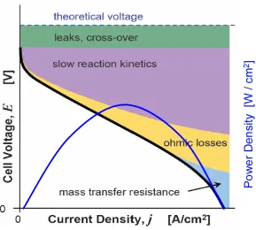
Various deleterious phenomena decrease the operating voltage from the theoretical Nernstian value, as depicted in the polarization curve of Fig. 1.2. A cell’s power output is defined as the operating voltage multiplied by the drawn current, meaning that these processes lower SOFCs’ power output. At open circuit conditions, leaks in the sealing that separate the anodic and cathodic compartments, as well as holes in the solid electrolyte, can allow fuel cross-over, which immediately lowers the
operating voltage. Also, non-zero electronic conductivity in the solid electrolyte has the same effect. Once current is drawn from the cell, three so-called overpotentials further decrease the operating voltage. Activation overpotentials are related to the finite-rate electrode reaction kinetics, and typically dominate the voltage losses. Ohmic
migrate throughout the cell. Concentration overpotentials arise when not enough reactants are supplied to the half-reaction sites, most often caused by mass transfer limitations in the gas phase, but these effects are only seen at very high current densities beyond practical operating conditions.
[image:26.612.181.470.72.332.2]Species’ transport through the crystal structure of metal oxides is generally thermally activated, and electrode kinetics are enhanced as temperature increases; therefore, high temperatures are desirable as they increase conductivity and reaction rates. Standard SOFC operating temperatures are anywhere from 700 – 1000 °C [5-6]. These high temperatures enforce strict requirements for component materials, even making choice of the interconnect material, which conducts the electrons to and from the respective electrodes, a complicated matter. In fact, the lack of cheap, viable options for
Fig. 1.2. A visualization of the overpotential losses typically encountered in SOFCs and the associated power density output of such a
high temperature interconnects has largely motivated the move toward intermediate operating temperatures, i.e., 500-650 °C. This is the point at which stainless steel and its derivatives can resist prohibitive oxidation, and could therefore conceivably be used for interconnects [13]. Furthermore, thermal cycling can lead to significant wear and tear due to differences in thermal coefficients of expansion, although it is less severe at lower temperatures.
Manufacturing scalability and its cost is a perpetual concern. Low-throughput, expensive fabrication processes cannot be a part of the final solution, although they can be useful toward more fundamental understanding. Similarly, catalytic materials can be used to impact and define sluggish reaction kinetic pathways, but they often consist of expensive, rare precious metals such as platinum or palladium [14]. Even though much lower operating temperatures can be achieved, this strategy is not viable on a large scale.
With so many aspects to SOFC technology, a methodical approach is needed to gain fundamental insights and elucidate the rate-limiting steps, eventually contributing to an informed, optimized design. From the brief overview above, two design focal points emerge—materials selection and cell architecture.
1.2.2 Materials Selection: Samaria-Doped Ceria (SDC)
Cerium(IV) oxide (or, ceria—CeO2-δ) has a cubic fluorite structure, capable of large
strictly 3+ cation dopant, such as samarium (SDC) or gadolinium (GDC). A samarium doping example is written here in Kröger-Vink notation:
𝑆𝑚2𝑂3+ 2𝐶𝑒𝐶𝑒𝑋 + 4𝑂𝑂𝑋 ↔2𝑆𝑚𝐶𝑒′ +𝑉𝑂∙∙+ 3𝑂𝑂𝑋+ 2𝐶𝑒𝑂2 (1.5)
This induces significant ionic conductivity at intermediate temperatures, garnering much interest for doped ceria as the SOFC electrolyte component [15-17]. Fig. 1.3 shows a conductivity comparison between common SOFC electrolyte materials, including the traditional favorite, yttria-stabilized zirconia (YSZ)[14]. A generally accepted benchmark for electrolyte conductivity is ~0.01 S cm-1, above which a candidate is deemed suitable. According to this metric, ceria-based electrolytes could potentially operate from 500 – 650 °C, without sacrificing performance, as would be the case with YSZ.
1000/T [K-1]
1.0 1.2 1.4 1.6 1.8
Log ( σ ) [ Ω -1 cm -1 ] -5 -4 -3 -2 -1 0
Temperature [ oC] 300 400 500 600 700 800 Ce 0.8Gd 0.2O 1.9 (ZrO
2)0.9
(Sc2O
3)0.1
(ZrO 2) 0.9(Y 2O 3) 0.1 (ZrO 2) 0.87 (CaO) 0.13 La 0.9Sr 0.1Ga 0.8Mg 0.2O
3-δ
BaZr0.9Y
0.1O3-δ
Bi2O3
(Bi,Y)2O3
Additionally, under the high temperature reducing conditions typically seen in a SOFC anode, intrinsic oxygen vacancies form spontaneously via the oxidation of lattice oxygen, according to [1]:
𝑂𝑂𝑋 ↔12𝑂2(𝑔) +𝑉𝑂∙∙+ 2𝑒′ (1.6)
These vacancies are charge compensated by electrons, which subsequently cause the cerium cations to change valence from nominally all 4+ to mixed 4+/3+. This gives rise to a non-trivial electronic conductivity via polaron hopping, making ceria a so-called mixed ionic-electronic conductor (MIEC). Although MIEC perovskite-type metal oxides are commonly employed as cathodes [18-20], there are few that are stable under the anode’s high temperature reducing conditions, and those that are have low conduction and/or slow hydrogen electrooxidation kinetics [21-23].
Due to the lack of available MIECs, a traditional SOFC anode is typically
composed of a random, three-dimensional amalgamation of an electronically conducting phase, e.g., nickel, an ionically conducting phase, e.g., YSZ, and a gas-permeable
itself, electrocatalytically active, and its bulk electronic conductivity is sufficient to place a current collector up to several microns away from a reaction site. Comparing the visualized anodes in Fig. 1.4b and d, it can be seen that a simple materials switch from YSZ to SDC affords a much greater reaction site density, owing to 2PB dominance over 3PB. In this way, materials selection paves the way for an architectural design paradigm, one where 2PB microstructures, rather than more restrictive 3PB microstructures, are possible.
1.2.3 Cell Architecture
Returning to the polarization curve of Fig. 1.2, there are three general design guidelines related to the three overpotentials outlined above. First, to reduce ohmic losses, all conduction pathways should be kept as short as possible. The primary culprit of ohmic
H2
O
2-H2O
2e
-YSZ
(ion conductor)
metal
10 nm 1 µm
metal
SDC
(ion and electron conductor) 10 nm
2e
-H2
O
2-H2O
1 µm
Fig. 1.4. Schematic diagrams of (a) the three-phase boundary (3PB) region where gas, metal, and yttria-stabilized zirconia (YSZ) phases intersect; (b) the 3PB density for a powder-processed anode; (c) the
two-phase boundary (2PB) region of a mixed ionic-electronic conductor like samaria-doped ceria (SDC); and (d) the 2PB density for the same anode as in (b), but with SDC instead of YSZ. Light blue areas indicate
electrochemically active regions.
(a) (b)
(c)
loss is oxygen ion transport through the solid electrolyte—the conclusion here is simple: make the electrolyte layer thin (µm scale). Second, for a given electrode reaction rate, maximizing the number of active reaction sites will increase the current density, on the basis of the projected area of the cell. For a MIEC anode like SDC, this effectively
translates into maximizing the active surface area (nm scale). Third, one must ensure easy gas phase access by highly porous, non-tortuous electrodes, although this is less of a concern than the previous two (µm and perhaps nm scale).
The ideal cell design must balance µm and nm length scales, which also means that new fabrication approaches must accommodate both. As SOFCs are high
temperature devices, care should be taken to ensure stability of any as-fabricated nanometer-sized features. Despite the obvious need for feature size reduction, a general hierarchical structure is desirable for aspects like electronic current collection—electrons cannot be expected to only travel through nanometer-sized metal films or multiple-micron-lengths of SDC without incurring severe resistance penalties.
subsequent ability to alter the design in accordance with the results. For instance, knowing the relationship between a SDC anode’s 2PB and its impedance spectra (c.f. Chapter 4) could lend valuable insight into which design knob to turn, and how much.
In summary, most operational voltage loss mechanisms in today’s SOFCs inform an overall feature size reduction of every component of the cell architecture. This move should be done intelligently, so as not to incidentally incur other penalties, e.g., gas diffusion limitations and bulk transport resistances, while at the same time maintaining manufacturability, scalability, and the ability to produce large total footprint cells. Furthermore, trending towards defined, as opposed to randomized, geometries can help link performance to tunable features.
As such, there is tremendous need and potential for entirely new SOFC design schemata, as well as complimentary fabrication techniques.
1.3
Anti-Dot Substrates: A New Design Framework
cm-2 [33]. Such significant microstructural differences can plausibly induce differences in reaction pathways. Accordingly, there is a pressing need to obtain geometrically defined electrode structures with tunable feature sizes that are more relevant to SOFC
electrocatalysis.
Demonstrated below is a facile fabrication strategy, known as polymer sphere lithography, in which monodisperse polymer spheres serve as sacrificial templates to construct anti-dot metal films (see Fig. 1.5a), permitting access to 3PB areal densities over an enormous range, from 2,000 to 43,500 cm cm-2. Though not previously explored in the fuel cell context, the anti-dot structure is ideal for advancing the aforementioned fundamental studies for this reason.
When these porous, metal films are overlaid onto an electrolyte substrate such as YSZ or SDC, the fraction of exposed electrolyte area and the 3PB are concurrently and specifically known, true for all two-dimensional lithographic processes. This enables electrocatalysis studies for the underlying electrolyte material, particularly as it pertains to 3PBs (and 2PBs for MIECs). The accessible 3PB regime here is previously untouched by conventional lithography, moving much closer to actually-in-use 3PB densities. Use in conjunction with diagnostic tools such as A.C. Impedance Spectroscopy (ACIS) allows definitive relationships between 3PBs/2PBs and various electrochemical activity-related materials characterization parameters to be established, e.g. rate limiting processes’ resistances, capacitances, etc. And when combined with traditional lithography
An even higher number of reaction sites can be achieved by moving from a planar to a three-dimensional structure, and these anti-dot films are a good starting point to get a variety of well-defined three-dimensional electrode structures.
Chapters 2 and 5 present the fabrication of the anti-dot structure and its derivatives, and Chapter 4 discusses the performance of its related SOFC electrodes.
1.4
Three-Dimensional Structures and Their Fabrication by CELD
Using the anti-dot structure as a starting point for the fabrication of high surface area three-dimensional structures, several specific, more optimized architectures can be considered, as in Fig. 1.5. Cathodic electrochemical deposition (CELD) is an ideal candidate to produce template-free high surface area structures, as well as templated frameworks like inverse opals (Fig. 1.5c and d) and nanowires/tubes (Fig. 1.5e). As a testimony to their flexibility, anti-dot based substrates can also accommodate new and old approaches such as screen printing [39], pulsed-laser deposition (PLD) [40], chemical vapor deposition (CVD) [41], and CELD (c.f. Chapter 3).
1.4.1 SOFC Fabrication Method/Morphology Non-Negotiables
Up to this point, only general SOFC materials/architectural design guidelines have been discussed, without reference to a particular method to produce such schemes. This section is devoted to the assessment of new fabrication techniques and their associated
as-produced morphologies, to aid in their development.
consistently produce the desired materials composition. Keeping large-scale
manufacturability in mind, basic repeatability is absolutely necessary. Second, the as-deposited morphology/microstructure cannot be adversely affected by SOFC operating conditions, e.g., high temperatures, oxidizing/reducing atmospheres, etc. This includes, for instance, cracking in electrolytes and agglomeration of small features in electrodes. Third, continuous and accessible migration pathways to and from surface reaction sites must exist in the electrodes. Of course, low resistance pathways are desirable, rather than only connected ones.
1 µm
1 µm SDC(ion and electron conductor) 1 µm
1 µm1 µm
SDC
(ion and electron conductor)
Fig. 1.5. (a) A schematic of a metal anti-dot network; (b) a cross-sectional depiction of the anti-dot film in (a) replacing metal powder as a current collector and thereby increasing the 2PB density; and examples of potential templated electrodes with tunable geometries like inverse opals (c) and (d), and nanowires (e).
(a) (b)
(c) (d)
In this manuscript, cathodic electrochemical deposition is evaluated as a components fabrication tool for a SDC-based, intermediate temperature SOFC.
1.4.2 Cathodic Electrochemical Deposition (CELD)
CELD is a liquid-based, low temperature fabrication technique that is able to produce ubiquitous and conformal metal oxide/hydroxide coatings of tunable surface area at low capital and operational costs [42-43]. The experimental setup is straightforward (see Fig. 3.2): three electrodes are immersed in a liquid electrolyte—electrons flow out of the anode and into the cathode through the external circuit, and the reference electrode measures the cell potential but does not allow any current to flow through it. A working potential is applied, and the appropriate electrochemical reactions occur.
Being liquid-based makes CELD scalable as a batch process, and allows easy control of large substrates, even if irregularly shaped: appropriate operating
for general SOFC applications [48-52], CELD ceria has been previously studied for corrosion protective coatings [46, 53-56], superconductor buffer layers [44], powder synthesis for increased sinterability [57], and nanowire/tube fabrication [49, 58-59]. Aside from ceria, other SOFC-relevant materials have been produced using this method, such as BaTiO3, Nb2O5, ZrO2, LaMnO3 [42], and Y2O3 [60].
There are two general categories of oxide/hydroxide electrochemical deposition, defined by which electrode experiences the desired deposition, known as the working electrode. Anodic electrochemical deposition (AELD) directly oxidizes Ce3+(aq) ions to insoluble Ce(IV) [54, 61-62]. A stabilizing ligand must be added to the electrolyte solution to ensure that Ce(III) species do not precipitate prematurely. A fundamental limitation of this technique is that Ce3+ ions must contact a surface that can conduct electrons away; as CeO2 is generally insulating, AELD should only be able to deposit extremely thin films, on the order of tens of nanometers.
Cathodic electrochemical deposition, on the other hand, proceeds by a two-step process. First, the electrolyte solution becomes progressively basic as electrochemical reduction reactions of various electrolytic species occur due to the applied cathodic potential at the cathode|electrolyte interface. This is widely referred to as
precipitation steps is given in Eqns. (1.7) and (1.8), respectively, although a myriad of possibilities exist (see Chapter 3 for an in-depth discussion).
𝑂2+ 2𝐻2𝑂+ 4𝑒− →4𝑂𝐻− (1.7) 𝐶𝑒3++ 3𝑂𝐻− → 𝐶𝑒(𝑂𝐻)
3 (1.8)
Chapter 2
Anti-Dot Substrates
2.1
Polymer Sphere Lithography Background and Summary
Polymer sphere lithography and, in particular, nanosphere lithography have gained recent attention for a wide range of applications ranging from novel nanofabrication techniques and photonic crystals to superhydrophobic surfaces [8, 63-64]. Most often, because the polymer spheres are typically not treated prior to metal deposition, the resulting patterned film is limited to isolated locations corresponding to the interstices between the template beads [7, 65-66]. With control of the fabrication process, however, the film may form a fully interconnected, yet fully porous network, acquiring what has been termed an ‘anti-dot’ configuration [67-68]. Specifically, an ordered layer of monodisperse polystyrene (PS) spheres is first applied to the surface of a SOFC electrolyte material; afterwards, the spheres are radially etched in an oxygen plasma, so as to create vias between them.Metal is deposited using a line-of-sight deposition method that enables the still-round PS to serve as a lithographic mask. Upon removal of the polymer template, the desired anti-dot porous structure is obtained. This process is illustrated stepwise in Fig. 2.1.
The periodicity provided by polymer sphere self-assembly is not critically important for SOFC studies; however, sufficient knowledge of microstructural parameters is required, as is high temperature stability. Accordingly, both factors are evaluated below.
approaches for monolayer deposition have been pursued in the literature, with varying degrees of complexity and experimental constraints. The most common methods are combined sedimentation plus evaporation [69-70]; spin-coating plus evaporation [71]; and controlled evaporation in combination with gradual substrate withdrawal from the solution (dip-coating) [72]. More exotic methods include electrophoretic assembly (suitable only to conducting substrates), and high pressure infusion in combination with ultrasonication [73-75]. While sedimentation, dip-coating, and spin-coating are relatively straightforward methods that produce structures with regularity sufficient for
electrocatalysis studies, they suffer from the tendency of the processes to yield regions with multiple layers and others entirely devoid of the polymer spheres. Furthermore,
Fig 2.1. The polymer lithography process, all on YSZ: (a) a monolayer of 500 nm polystyrene (PS) spheres; (b) diameter of spheres reduced via oxygen plasma etching; (c) metal (Cu) deposited by thermal
evaporation; (d) PS spheres removed.
(a)
(c)
(b)
achieving adequate control of the evaporation step for the former two can require
excessive processing times. With the exception of a dip-coating setup encased to provide strict humidity control [72], these methods have difficulty spanning the nanosphere-microsphere range; that is, any given polymer sphere deposition method works with either nanospheres or microspheres, but not both (note: PS spheres less than 1 µm in diameter are herein referred to as nanospheres, whereas spheres greater than 1 µm are referred to as microspheres).
Here, spin coating is employed as a facile means of obtaining the desired
monolayers on YSZ and SDC substrates, where a slight variation of the standard spinning approach is necessary for microspheres. Utilization of electronically insulating substrates precludes electrodeposition as a means of subsequent growth of the metallic film,
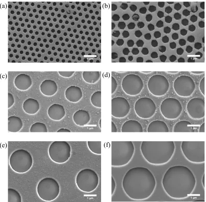
Fig 2.2. Selection of representative copper anti-dot metal films on YSZ showing a range of feature sizes achieved using polymer sphere lithography: (a) 500 nm initial bead size; (b) 790 nm initial bead size;
(c) 2 µm initial bead size, heavily etched; (d) 2 µm initial bead size, lightly etched; (e) 3.2 µm initial bead size, heavily etched; and (f) 3.2 µm initial bead size, lightly etched.
(a)
(b)
(c)
(d)
2.2
Experimental Details
2.2.1 Substrate Preparation
The YSZ substrates (MTI Corporation) used are (100) single-crystals, and the SDC substrates are epitaxially deposited thin films on single-crystal YSZ via pulsed laser deposition [32]. For subsequent use for nanosphere deposition, the substrates were exposed to an oxygen plasma for 5 minutes at 75 W and 250 mTorr (Technics Planar Etch II) to enhance hydrophilicity. In contrast, as-purchased or as-fabricated substrates were directly used for microsphere deposition.
2.2.2 Nanosphere Deposition
Monolayers were spun using a Laurell, WS-400B-6NPP/LITE spin coater, with a 10 wt% suspension of PS nanospheres, surface functionalized with carboxyl groups (Bangs Laboratories, Inc.™). Before spin coating on the substrate, the as-received PS suspension is sonicated to ensure the beads are homogeneously dispersed. Exactly 35 µL of the suspension was manually spread over the entire 1 cm x 1 cm substrate before spinning. The final RPM of the spin coater was 3000 RPM, with varying accelerations depending on the starting PS diameter. The PS monolayer was radially etched in the same oxygen plasma system, but at elevated powers (75 – 200 W). In this step, the beads do not move from their original positions. Typical etching times were anywhere from 5 – 20 minutes.
2.2.3 Microsphere Deposition
spun as before. The spin coater was spun at 4000 RPM. A standard laboratory spray bottle was used to employ the water-wash method, described in detail in Section 2.3.2. If the spin-wash-dry cycle was repeated too many times, immovable multilayers would form. For the 2 µm spheres, the cycle was repeated 3 times; for the 3.2 µm spheres, the cycle was repeated 6 times.
2.2.4 Metal Deposition
An in-house constructed thermal evaporation system was used to deposit copper, nickel, titanium, titanium/gold, or aluminum (Alfa Aesar, 99.98+%) at 10-5 Torr. Platinum networks were evaporated using an electron beam evaporator (re-manufactured CHA MK-40). The now covered PS beads were removed with an acetone-soaked cotton swab; regardless of the metal deposited, the surface became lustrous after wiping repeatedly, indicating the PS was gone.
2.2.5 Microstructure Analysis
pore areas were assumed to be perfectly circular, and the diameters were calculated from the individual pore areas.
2.2.6 High Temperature Stability
Nickel networks 200 nm thick were brought to 600 ºC under flowing 98.7% H2 and 1.3% H2O and held there for 50 hours.
2.3
Results and Discussion
2.3.1 Nanosphere Lithography Results
the porous film. These considerations preclude fabrication of useful anti-dot electrodes with PS spheres of less than 500 nm in diameter. Fig. 2.4 shows that qualitatively similar coverage is achievable with a variety of different PS sphere diameters.
2.3.2 Microsphere Lithography Results
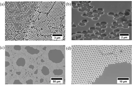
In contrast to the deposition of nanospheres, no set of conditions could be identified for the preparation of a comprehensive monolayer of PS microspheres using a single spin-coating step. Under all accessible spinning conditions, functionalized PS microspheres assembled into irreversible multilayers (see SEM images in Fig. 2.5) that could not be modified for further use due to the line-of-sight nature of the metal deposition step. If metal deposition was pursued regardless of the presence of multilayers, unacceptable
levels of irregularity in the anti-dot films resulted, as in Fig. 2.5b. In contrast, at high spinning rates, non-functionalized PS microspheres formed monolayers, but with only partial coverage (see Fig. 2.5c), whereas at lower spinning rates multilayer regions emerged (particularly towards the edge of substrate), without elimination of the void areas. A low magnification optical image of such a dilemma is shown in Fig. 2.6, where multilayer regions (white portions) mark the border of the substrate, as well as covering a little less than half of the remaining interior; and void regions (dark areas, more easily seen in Fig. 2.6b) litter the entirety of the interior. The thick multilayer border region is of particular concern, as it can constitute up to 10% of the total substrate.
(a)
(b)
(c)
As an alternative to a single-step monolayer deposition procedure, a process was Fig 2.5. (a) Irreversible multilayers formed after a single spin coat of functionalized PS microspheres; (b)
the resulting metal film porosity suffers from such multilayers; and (c) and (d) a single spin coat of non-functionalized PS microspheres formed monolayers on most parts of the substrate, but with a significant
number of voids.
(a)
(c)
(b)
[image:48.612.113.540.69.345.2](d)
Fig 2.6. Optical photographs of the entire 1 x 1 cm YSZ substrate (a) and a zoomed in view of one corner (b) with a single spin coating of PS microspheres. The white regions are multilayers, the light
gray regions are monolayers, and the dark regions are voids.
developed employing multiple spin-coating steps of the non-functionalized PS beads, depicted in Fig. 2.7. Specifically, a substrate for which the first deposition has yielded a mixture of void regions, monolayer regions and multilayer regions is gently rinsed with water to remove the excess layers in the multilayer regions and the spin-coating is repeated to induce deposition in the void regions. The process is repeated multiple times until the void regions constitute less than about 10% of the substrate area, beyond which multilayer regions cannot be removed by a gentle rinse with water. In a final step, a small amount of the PS suspension is directly applied to the substrate and allowed to dry, eliminating the remaining void regions but with unordered sphere arrangement, as opposed to the relatively periodic arrangement produced by spin coating. For this reason, the spin coating step is repeated as many times as possible before this last step is applied, as disorder in the PS monolayer undoubtedly affects the 3PB/2PB densities. Fig. 2.8 exhibits the most extreme case of utilizing only one spin coat run, resulting in a large portion of the substrate being disordered.
Fig 2.7. (a) The water-wash method utilizes sequential spin coats with water-washing in-between steps. 2 µm beads shown here on a standard 1 x 1 cm YSZ substrate; (b) an optical photograph showing comprehensive monolayer coverage over the entirety of the substrate after the final multilayers are washed
off, and a magnified SEM image of a monolayer of 2 µm beads.
Fig 2.8. Optical and SEM images showing the result of utilizing only one spin coat step in the water-wash method. The darker regions in the SEM image correspond to relatively ordered arrangements of PS beads from the spin coat step; alternatively, the lighter regions correspond to unordered arrangements from the
final evaporation step. The substrate shown here is 1 x 1 cm YSZ with gold metal.
(a)
By this method, it was possible to prepare comprehensive monolayers of PS beads up to 3.2 µm in diameter with the same coverage quality as the nanospheres (compare the nanosphere coverage of Fig. 2.4 to the microsphere coverage of Fig. 2.9). After the microsphere monolayer deposition is complete, the subsequent plasma treatment, metal deposition and template removal steps then proceed as described for the nanosphere lithography, where, again, a minimum of ¼ of the bead diameter must be removed in order to prevent necking during oxygen plasma treatment.
2.3.3 Microstructural Fidelity
Given the importance of three-phase boundaries for SOFC electrocatalysis, the 3PB areal density is a key parameter describing the microstructural features of these or any fuel cell electrode. A further important parameter in the case of the two-dimensional electrodes prepared here is the metal coverage, or inversely, the fraction of exposed electrolyte area, i.e., the 2PB areal density. With knowledge of these two parameters and an ability to tune them over a wide range, it becomes possible to achieve the goal of deconvoluting
microstructural and compositional influences on electrocatalysis rates.
Fig 2.9. Monolayer substrate coverage via multiple spin and wash cycles of polystyrene microspheres on YSZ: (a) 2 µm, and (b) 3.2 µm. Both images contain ~1200 beads.
For a perfect micro-/nanosphere lithographic process in which the template beads display ideal periodicity over the entirety of the substrate, both the 3PB areal density,
𝜌3𝑃𝐵, and the 2PB area fraction, 𝑓2𝑃𝐵, can be computed from knowledge of the starting bead size and the extent of size reduction induced upon plasma etching. The theoretical values of these two quantities are given in equations 2.1 and 2.2, respectively, as functions of the initial (𝜙𝑖) and final (𝜙𝑓) diameters of the PS beads.
𝜌3𝑃𝐵𝑡ℎ𝑒𝑜 =2𝜋√3�𝜙𝜙𝑓𝑖�𝜙1𝑖 (2.1)
𝑓2𝑃𝐵𝑡ℎ𝑒𝑜 =2√3𝜋 �𝜙𝜙𝑓𝑖� 2
(2.2)
For an imperfect fabrication process, many kinds of defects exist—disordered regions of PS beads, multilayer and void areas (areal defects); grain boundaries between ordered regions (line defects); and singly missing PS beads within an ordered region (point defects). To assess the influence of these random structural elements, a continuous string of scanning electron microscopy (SEM) images (typically numbering from 100-400 images per sample) was collected from border to border for four representative films. From each image the following parameters were determined: the number and diameter of the pores, the metal|substrate interface length, i.e., 3PB length, and the exposed
electrolyte area fraction, i.e., 2PB area fraction. The film characteristics and measured results are summarized below in Table 2.1 and Figures 2.10 and 2.11.
0.0 0.5 1.0 1.5 2.0 2.5 3.0 0 2000 4000 6000 8000 10000 12000
0.0 0.5 1.0 1.5 2.0 2.5 3.0 0 2000 4000 6000 8000 10000 12000
0.0 0.5 1.0 1.5 2.0 2.5 3.0 0 1000 2000 3000 4000 5000 6000 0.0 0.5 1.0 1.5 2.0 2.5 3.0 0 40000 80000 120000 160000 Count s
Effective Pore Diameter / µm
C
ount
s
Effective Pore Diameter / µm Effective Pore Diameter / µm
C
ount
s
Effective Pore Diameter / µm
C
ount
s
Fig 2.10. Pore diameter histograms of copper networks on YSZ, reflecting the different starting PS bead sizes: (a) 500 nm etched to 300 nm; (b) 2 µm etched to 1.29 µm; (c) 2 µm etched to 1.58 µm; (d) 3.2 µm
etched to 1.72 µm.
0 20 40 60 80 100 0 2 4 6 8 10 12 14 16
0 20 40 60 80 100 0 2 4 6 8 10 12 14 16 0 20 40 60 80 100 0
10 20 30 40
0 20 40 60 80 100 0 4 8 12 16 20 Count s
2PB Area Fraction (%)
2PB Area Fraction (%)
C
ount
s
Count
s
2PB Area Fraction (%) 2PB Area Fraction (%)
C
ount
s
Fig 2.11. 2PB area fraction histograms of copper networks on YSZ, reflecting different starting PS bead sizes: (a) 500 nm etched to 300 nm; (b) 2 µm etched to 1.29 µm; (c) 2 µm etched to 1.58 µm; (d) 3.2 µm etched to 1.72 µm. Solid and dashed lines indicate the average and theoretical values, respectively.
pores represented in the histograms of Figure 2.10, a small number of pores with large diameters, > 3 µm, was also observed. These are taken to reflect regions in which
multilayers of PS beads occurred, which prevents metal deposition over larger areas (c.f. Fig. 2.5b). For the PS with an initial diameter of 2 µm, the number of these multilayer-induced pores is less than 1% of the total; for the 3.2 µm initial diameter spheres, the number is less than 0.5%; and for the 500 nm spheres, the number is less than 0.1%. Aside from their statistical insignificance, the contribution of these large diameter pores to the overall 𝜌3𝑃𝐵 is confirmed to be small, as indicated by the good agreement between the theoretical and experimental values of this parameter, Table 2.1, and they are omitted from the plotted range for clarity.
The image-to-image variation in the 2PB area fraction (Fig. 2.11) shows that the variability in 𝑓2𝑃𝐵 is more significant than the pore diameter variability. The widest distribution in 𝑓2𝑃𝐵is evident for the film prepared using 500 nm PS beads, where the standard deviation is 12% of the substrate area (i.e., 𝑓2𝑃𝐵is 31.5 ± 12.0%). Moreover, in all cases, the observed 2PB area was lower than that computed from the initial and final
Table 2.1.Comparison of theoretical and experimental 3PB length areal density and percent 2PB exposure for different initial PS bead diameters.
Initial bead
diameter,
𝝓𝒊/µm
Final pore
diameter,
𝜙𝑓/µm
Pore diameter
Gaussian
width/µm
Theoretical
3PB length
density/m cm-2
Experimental
3PB length
density/m cm-2
Theoretical percent 2PB exposure Experimental percent 2PB exposure 2PB exposure standard deviation
0.5 0.3 0.06 435 406 32.6% 31.5% 12.02
2 1.29 0.07 117 112.8 37.7% 33.4% 6.70
2 1.58 0.08 143 137.3 56.6% 49.7% 4.69
PS sphere sizes. This can be attributed to the occurrence of point and line defects in the PS two-dimensional crystals, as well as the presence of disordered regions in the monolayer. The statistics surrounding the two films prepared using PS beads with an initial diameter of 2 µm suggest that line and point defects become increasingly important as the extent of etching is minimized. In the case of the film obtained from lightly etched
PS beads (𝜙𝑓 = 1.58 µm) there is a large difference between 𝑓2𝑃𝐵𝑡ℎ𝑒𝑜 and 𝑓2𝑃𝐵𝑒𝑥𝑝 (56.6 vs.
49.7 %). When the beads are more heavily etched (𝜙𝑓 = 1.29 µm), the difference
decreases, whereas the difference between 𝜌3𝑃𝐵𝑡ℎ𝑒𝑜 and 𝜌3𝑃𝐵𝑒𝑥𝑝 and the distribution of pore
sizes for the two films are essentially the same. This behavior can be understood as follows. In the case of the lightly etched film, isolated missing beads (both point defects and dislocations behave as isolated, absent beads in a two-dimensional crystal) become a significant portion of the open area available for metal deposition, and, in this manner, such defects increasing in number dominate the coverage features.
The histograms of 2PB area display significant numbers of occurrences outside of what is roughly the main peak. As already indicated, regions with 2PB area below the mean occur as a consequence of defects in the two-dimensional crystals, i.e., voids in the PS bead array, whereas regions with higher fractions of 2PB area occur because
multilayers form during the PS bead deposition process, i.e., excessive coverage of the substrate with PS beads. The 500 nm diameter nanospheres generate films in which slightly less than 10% of the regions display significant PS bead void areas, whereas 4% display multi-layered areas. In contrast, for both sizes of microspheres (2 and 3.2 µm) the regions affected by voids in the PS bead array are less than 5%, indicating that the
occurrence of multilayer regions for the 2 µm microspheres accounts for 11% of the regions imaged, whereas for the 3.2 µm it is only 1%, suggesting that multi-layer removal becomes facile as the bead size increases.
Overall, despite the imperfection of the monolayer deposition process, the theoretical and experimental values, respectively, of 𝑓2𝑃𝐵 and of 𝜌3𝑃𝐵 agree quite well with one another, indicating that the fabrication is, in fact, rather controlled. Indeed, all of the experimental 𝜌3𝑃𝐵 values are within 93% of the theoretical, and this was found to hold irrespective of substrate employed or metal deposited. Accordingly, the geometric features of any sample prepared by the methodology presented here can, within a reasonable degree of certainty, be predicted from knowledge of 𝜙𝑖 and 𝜙𝑓.
2.3.4 Thermal Stability
Fig 2.12. Images of an anti-dot porous nickel network (a) and (c) before thermal treatment at 600 ºC under hydrogen (pH2 = 0.1 atm); and (b) and (d) after thermal treatment. (a) and (b) are top-down SEM images;
(c) and (d) are AFM images.
(a)
(c)
(b)
Chapter 3
Cathodic Electrochemical Deposition of
Undoped and Doped Ceria
3.1
Introduction
There are numerous reports in the literature regarding the CELD of ceria [45-46, 53, 55, 57, 77-83], including a handful that generally list SOFCs as potential applications, but with limited demonstration [48-52]. In addition, the contribution of electrogeneration of base to CELD is well-documented [42-43]. However, insight related to the crucial SOFC design criteria outlined in Section 1.4.1 is incomplete as most reports focus on
as-deposited composition and characterization, which is a broad area of study by itself due to the large parameter space. Aside from grain growth evolution and brief mention in a few studies, high temperature data are largely missing [49-51, 78, 80, 83]. Perhaps most importantly, the vast majority of reports utilize non-porous, purely metallic substrates, which violate the continuous pathway for ionic species requirement. To the best of the author’s knowledge, a composite conducting/non-conducting substrate is mentioned only once as a part of a larger study, in which the CELD of ceria was performed on a
nickel/yttria-stabilized zirconia cermet, but was not explored in detail [45]. Therefore, this study assesses CELD according to (1) its compositional control, (2) the high temperature behavior of its coatings, (3) its ability to meet minimum SOFC
configurational requirements, and (4) its potential for wide-ranging microstructural optimization. In so doing, the electrogeneration of base/chemical precipitation
new insights are gained regarding the roles of the working potential and the depositing species to the resulting microstructure, allowing a predictive, instead of haphazard, approach to future CELD work.
In order to explore the flexibility of CELD as a fabrication tool, a range of deposition conditions were examined, and a correspondingly wide range of reproducible morphologies were obtained. Rather than describe the entirety of those results, two primary types of morphologies are reported here—high surface area (HSA) coatings and thin, planar films. These two microstructures are evaluated in the context of the HSA coatings’ ability to be used as electrode components and the thin, planar films’ ability to be used as electrolyte components.
As a visual aid to understand the general deposition mechanism and to distinguish between the two experimental conditions probed in this chapter, a Ce-H2O-H2O2
applied potentials are used for the two morphologies, regardless of the composition of the electrolyte solution.
3.2
Experimental Details
3.2.1 Substrate Definition
The primary type of substrates used was a composite substrate, comprised of a supporting YSZ base, on top of which various kinds of porous metal networks are overlaid. The
Fig. 3.1. Pourbaix diagram for the Ce-H2O-H2O2 system, reprinted with permission from [86]. The black arrow on the right-hand side, vertical axis represents a typical HSA depositing potential (-0.8 V
pores in the metal films are necessary to allow for oxygen ion flux, and connectedness in the metal networks is necessary to provide electronic conduction.
All reagents obtained were research grade. YSZ single-crystals (MTI Corp.), 1 cm x 1 cm x 0.5 mm, oriented (100) are used as the supporting substrates. On the surface of the YSZ, two primary porous metal network configurations are used. One, 400 nm thick nickel anti-dot films are made via polymer sphere lithography (Fig. 3.2a), the details of which are described in Chapter 2 of this manuscript. Two, 200 nm thick parallel platinum strips are made via conventional photolithography (Fig. 3.2b), obtained from Dr. Yong Hao, whose work is described in detail elsewhere [31]. The strips are electrically
connected to one another by a platinum border near the edge of the YSZ substrate. Here, the widths of the platinum strips are made identical to each other and to the open spacing
(a)
(c)
(b)
Fig. 3.2. Interconnected nickel anti-dot network (a), photolithographically defined platinum strip network (b), and platinum paste network (c) on single-crystal YSZ supporting substrates. The darker regions of each
42
between them, denoted by the shorthand 5-5µm and 10-10µm, indicating that the widths are 5 and 10 µm, respectively. It should be mentioned that these lithographic networks allow both the metal and exposed YSZ surface areas to be specifically known, to a high degree of accuracy.
One additional, thicker metal network configuration is used, but only to test the high temperature annealing behavior of the deposits (Fig. 3.2c). Platinum paste
(Engelhard 6082) is spread across the entire YSZ surface and allowed to dry for two hours, and then heat treated at 400 °C for 1 hour and 900 °C for 2 hours at 1 °C min-1 to remove residual organics and sinter the platinum particles together. This results in a spider-web-like network of platinum with feature sizes on the order of microns, necessary to prevent metal coarsening at higher temperatures from damaging the deposits.
To obtain large amounts of the deposits for bulk studies, 0.25 mm thick nickel foil substrates are used with depositions performed at 0.8 mA cm-2 for 1-2 hours. The
powdery deposits are subsequently scraped off of the nickel foil and gathered for analysis. Also, in order to image cross-sections of the thin film deposits, 350 – 400 nm thick nickel films are thermally evaporated onto 1 x 1 cm silicon substrates.
3.2.2 Experimental Setup