University of Twente
Faculty of Electrical Engineering,
Mathematics & Computer Science
Charge Steered RF PA
Erik Olieman
MSc. Thesis
August 2010
Supervisors:
prof. dr. ir. B. Nauta
dr. ir. A.J. Annema
dr. ing. E.A.M. Klumperink
Report number: 067.3372
Chair of Integrated Circuit Design
Faculty of Electrical Engineering,
Mathematics & Computer Science
University of Twente
iii
Summary
This master thesis describes the development of a new type RF PA and upconverter combination. Instead of the normally used voltage steering the amplifier uses charge steering. The parasitic
capacitances of the MOSFET in combination with using charge steering form a feedback network that linearizes the amplifier.
The developed device is a switching amplifier. For good behavior it uses a capacitor to be able to quickly inject high amounts of current. Derived equations show that feedback becomes better if the gate-drain capacitance is relative large compared to the gate-source capacitance. For this reason a capacitor is periodically placed between the gate and the drain terminals of the amplifying transistor using switches. Half of the time this capacitor is placed there, during this time the charge present on the capacitor determines the output voltage. The other half of the time the amplifying transistor is turned off.
The designed RF power amplifier and upconverter combination is designed in 65nm CMOS and operates at a center frequency of 1GHz. The maximum output power is 17.5dBm, its 1dB
compression point is only 0.6dB below its maximum output. Up to this output power also two-tone tests perform well, the worst in-band IMD3 component is at -29dBc at an amplitude equal to the 1dB compression point. An efficiency of 21% is reached at the 1dB compression point.
Charge injection by the switches decreases performance for lower output values, the range of powers across which the amplifier performs well is around 20dB. The maximum is the 1dB
compression point, so the minimum power, where charge injection becomes a significant problem, is 20dB below the 1dB compression point.
v
Contents
1 Introduction ... 1
1.1 Amplifier types ... 1
1.2 Project description ... 1
1.3 Contents ... 2
2 Principle ... 3
2.1 Equations ... 4
2.1.1 Basic ... 4
2.1.2 Output impedance... 5
2.1.3 Quadratic analysis ... 5
2.1.4 Mobility reduction ... 6
2.2 Capacitances ... 9
3 Top level design ... 11
3.1 Location of charge injection ... 11
3.2 Charging the capacitor ... 12
3.3 Carrier suppression ... 14
3.3.1 Shifting up ... 15
3.3.2 Differential ... 16
3.3.3 Phase of the switches ... 18
3.3.4 Conclusion ... 20
3.4 Steering... 21
3.5 Complete amplifier ... 22
4 Design ... 23
4.1 Amplifying transistor ... 23
4.1.1 Output impedance... 24
4.2 Injection capacitor ... 24
4.3 Input current source ... 24
4.3.1 Dimensions ... 26
4.3.2 Behavior ... 26
4.4 Auxiliary voltage source ... 28
4.5 Switches ... 29
4.5.1 Switch 1 ... 30
4.5.2 Switch 2 ... 30
4.5.3 Switch 3 ... 31
4.5.4 Charge injection due to switches ... 32
4.6 Switch control voltages ... 34
vi
4.7 Output filter ... 36
4.7.1 Inductors ... 38
4.7.2 Component values ... 38
4.8 Threshold voltage source ... 39
5 Simulation results ... 43
5.1 Linearity ... 43
5.1.1 1dB compression point ... 43
5.1.2 Intermodulation distortion ... 45
5.2 Efficiency ... 48
5.2.1 Power consumption per component ... 48
5.3 Inductor quality factor ... 50
5.4 W-scaling ... 50
5.4.1 Efficiency ... 51
5.4.2 Linearity ... 51
5.4.3 Output impedance... 52
5.5 Threshold voltage ... 53
5.6 Comparison with published Pas ... 54
6 Conclusion ... 57
6.1 Recommendations... 58
7 Bibliography ... 59
Appendix A: Equations ... 61
A.1 Basic ... 61
A.2 Output impedance ... 62
A.3 Quadratic analysis ... 62
A.4 Mobility reduction ... 63
1
1
Introduction
Low power consumption is critical for portable systems to achieve good battery life. Power
consumption in wireless systems is typically dominated by the RF power amplifier (PA), so a PA with a high efficiency is critical.
Switch mode power amplifiers with constant envelope output can achieve high efficiencies, however they can only amplify constant envelope modulation schemes, while most modern modulation schemes do not have constant envelopes. This allows for more efficient use of the spectrum and high data-rates, but comes at the cost of high linearity requirements. Nonlinear behavior causes distortion products in adjacent channels, lowering the percentage of the spectrum that can be used by other devices, and in-band distortion, lowering the achievable data-rate.
Linearity and efficiency can be exchanged for one another, so the goal is to design a system with both a high linearity and good efficiency.
1.1
Amplifier types
RF power amplifiers can be divided into two groups, linear and switching amplifiers. They are further divided into different classes: A, B, C, D, etc.
Linear amplifiers have an output that is at least partly sinusoidal. Class A, AB, B and C belong to the linear amplifiers. They differ in the time a transistor conducts, the conduction angle, from 100% in class A amplifiers till less than 50% in class C amplifiers. A lower conduction angle increases the efficiency, but at the cost of linearity.
Linear amplifiers can reach an arbitrary linearity by decreasing the output swing. However again, this causes a steep decline in efficiency.
Switching amplifiers do not attempt to create a sinusoidal output, they create a square wave. The output filter removes higher harmonics while keeping the first harmonics. This allows for a theoretical efficiency of 100%. A fully switching amplifier can only be used in constant envelope modulation schemes. By modulating the supply voltage also the output amplitude is modulated. In theory it would still be possible to have 100% efficiency by using a class D amplifier to modulate the output amplitude, but in practice the efficiency will decrease. Time delay between the modulation of the supply and the switch signal, together with the finite bandwidth of the supply modulation gives rise to distortion products, even when everything else is ideal. Since both these effects are related to the bandwidth of the RF output, the performance is limited for high bandwidth systems.
In this project a switching amplifier is developed that uses direct feedback to obtain a good linearity. This way it should be able to combine the high efficiency of switching amplifiers with the good linearity of linear amplifiers.
1.2
Project description
RF power amplifiers generally use voltage control; the intrinsic capacitances of the transistor only decrease the efficiency since they have to be charged and discharged, while they provide no benefits. For this master thesis the possibility for using charge/current control instead is investigated. Here the intrinsic capacitances form a feedback network that can linearize the transistor. Since the
2
1.3
Contents
3
2
Principle
RF power amplifiers generally employ voltage steering. The schematic shown in Figure 2-1 is the general circuit usually used by voltage steered power amplifiers.
L
choke
Antenna
V
CC
Z
matching
V
in
Figure 2-1: Voltage steered RF PA architecture
The gate is controlled by a voltage source. A transistor amplifies the input voltage and via a matching circuit an antenna is connected. This basic circuit can be used for many different operation modes, but some principles stay the same. The voltage source puts a voltage on the gate that is independent of everything else.
The basic principle of a charge steered PA instead of a voltage controlled PA is shown in figure 2-2.
C
GD
Z
load
C
GS
I
in
Feedback
Gain
4
Instead of a voltage at the gate, now a charge is applied on the parasitic capacitances of the transistor. When the drain voltage increases, the gate voltage will also increase via the voltage divider and . The increase in gate voltage results in an increase in drain current, which decreases the drain voltage. Hence this mechanism provides negative feedback and has as result that the output voltage is relative independent of the transconductance of the transistor, in contrast to voltage steered amplifiers that do not have this feedback.
2.1
Equations
To get a more accurate impression of a charge steered amplifier relations are derived with various levels of accuracy that describe that behavior of the amplifier. First a highly simplified version is derived, followed by more accurate ones.
2.1.1 Basic
First the small signal response of the amplifier is calculated. The individual steps are explained in the appendix, section A.1. The output voltage is given by:
( 2-1 )
The input voltage can also be related to the charge present on the capacitors.
( 2-2 )
The charge in the gate-drain capacitance is given by the capacitance and the voltage across it.
( 2-3 )
Combining (2-2) and (2-3) and rewriting them gives:
( 2-4 )
Combining (2-4) and (2-1) gives the output voltage as function of input charge.
( 2-5 )
When the output resistance of the transistor is taken into account, (2-5) turns into:
( 2-6 )
For an infinite transconductance, the voltage gain would be infinite, just like the ideal situation for an OpAmp, this reduces (2-6) to:
( 2-7 )
5
2.1.2 Output impedance
The output impedance of a circuit is given by (2-8).
( 2-8 )
Combining this with (2-6) allows us to calculate the output impedance of the circuit.
( 2-9 )
A larger transconductance results in a lower output impedance. This was expected since feedback will lower the output impedance, and a higher transconductance implies a larger loop gain, so more feedback.
2.1.3 Quadratic analysis
It is interesting to analyze how the linearity of the system depends on how the transistor is controlled. For this the same method is used as in section 2.1.1. However now the drain current is assumed to have a quadratic dependency on the input voltage. This is a useful approximation since the basic MOST model is a quadratic relation between input voltage and output current.
( 2-10 )
Using the same methodology as in section 2.1.1 and some extra steps to simplify the result, the resulting output voltage becomes:
( 2-11 )
( 2-12 )
To compare this to the voltage steered case a Taylor approximation is calculated. Since we want to compare the second order harmonics we need the corresponding component in the Taylor series. The second order term in the Taylor series is noted as . For both the voltage and charge steered situation is divided by the load impedance, so the second order component in the drain current can be compared directly.
For the charge steered version the input charge is substituted by the corresponding input voltage.
( 2-13 )
Using (2-13) the second order coefficient of the drain current of the charge steered circuit is given by equation 2-14.
( 2-14 )
6
( 2-15 )
Compared to the voltage steered version, it is clear that the second order distortion of the charge steered circuit will always be lower. As expected the linearity increases with the loop gain. When the same analysis is done for the first harmonic around the result is that they are identical, this is expected since in the linear case the charge steered PA has an output equal to the voltage steered PA when (2-13) is substituted in the relation between input charge and output voltage (2-142-11).
Equation 2-11 shows a potential problem: The dependency between output voltage and input charge includes a square root, which has an infinite Taylor series. So while the voltage steered amplifier would only have second order distortion, and hence has no in-band intermodulation distortion, the charge steered amplifier does have intermodulation distortion. So in order to be able to compare intermodulation products a more accurate analysis is required where both the voltage and charge controlled versions have intermodulation distortion.
2.1.4 Mobility reduction
In order to find the effect of charge steering on (third order) intermodulation distortion, a transistor model that includes higher order components in the output current than the square law model previously used is required. It was found that mobility reduction is one of the major causes of non-ideal behavior in MOSFETs [1]. The square law relation for the drain current with mobility reduction added is shown in equation 2-16. This formula also covers velocity saturation, which only adds an extra factor to θ.
(2-16 )
This results in high order distortion in both the voltage and charge controlled versions, enabling a fair comparison between these two.
The output voltage when charge steering is used is equal to:
( 2-17 )
is given in (2-12).
The Taylor expansion of (2-16) times and of (2-17) are both calculated and used to compare the linearity. For a fair comparison a principle similar to the OIPX is required, so (2-18) is used:
7 This equation is, minus some scaling factors, the same as what is used to calculate the OIPX, where X
is the order of the distortion that we want to look at, while is the Y’th order behavior, which is calculated by the Taylor expansion.
As discussed earlier, the resulting equations are too large to be useful for symbolic comparisons. For that reason they are compared numerical. The used values are:
50Ω 2pF 1pF 0V
2.6
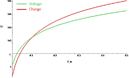
These values correspond roughly to a thick oxide transistor in 65nm CMOS with dimensions of 50x40μm/0.28μm. Only the threshold voltage is set at zero for simplicity, since it only results in a shift it does not affect the comparison. The corresponding θ value is around 2. For comparison also higher and lower θ values are used.
[image:13.595.75.516.376.642.2]First a θ of 2 is used, corresponding to a reasonable amount of third order distortion. The result for third order products, calculated from (2-18) is plotted below; higher corresponds to a better linearity.
Figure 2-3: Linearity regarding third order intermodulation products for θ =2
8
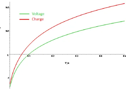
[image:14.595.81.514.157.468.2]inputs, and a lot of second order distortion that is converted to third order distortion by intermodulation.
Figure 2-4 shows the same for second order distortion. Here the charge steered version is always better, but this is not as important as third order distortion.
Figure 2-4: Linearity regarding second order intermodulation products for θ =2
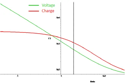
When the third order products compared to the linear products are plotted again, but for a much lower θ value, the problem with second order distortion is clearer; figure 2-5 shows this.
For and a low value for θ the amount of third order components in the transconductance is much lower. The amount of second order distortion transformed into third order by the charge steered transistor stays roughly equal, so this is dominant and for low values of θ the third order distortion in the charge steered circuit approaches a minimum value due to this, while this does not happen in the voltage steered circuit.
9 Figure 2-5: Linearity regarding third order intermodulation products for Vin=0.3V, dashed line represents nominal θ
It can be concluded that for devices that have a behavior close to the ideal square-law relation charge steering does not offer advantages. However when the behavior moves away from the square-law behavior with more non-idealities, the charge steering has better linearity, especially when the loop gain is high.
2.2
Capacitances
Until now it was assumed that the capacitances of a MOSFET have a fixed value, which is not the case. Since the transfer function in case of charge steering depends mainly on the capacitances it is important to know their behavior. In this paragraph the sources of the capacitances and their behaviors are discussed.
The parasitic capacitances of MOSFETs come from three sources [2][3]: Intrinsic capacitances
Extrinsic capacitances Junction capacitances
The intrinsic capacitances are those due to the channel. They are highly bias dependant, since they depend on the depletion and inversion layer shape and size.
Extrinsic capacitances are relatively bias independent. They are for example the overlap capacitances between the gate and the heavily doped source and drain connections.
10
Figure 2-6: MOSFET capacitances
The two most important capacitances of a charge steered amplifier are the gate-source and especially the gate-drain capacitance: they directly affect the transfer function. The drain-bulk capacitance is also relevant since it needs to be charged and discharged by the amplifier continuously, so it affects the efficiency.
The gate-drain capacitance is the sum of its intrinsic and extrinsic capacitances. The intrinsic
capacitance is largely non-existent in saturation; there is not much of an inversion layer at the drain side of the transistor in saturation. When the device is turned off it is also not present, only when it enters triode the intrinsic capacitance becomes significant.
What remains is the overlap capacitance, the capacitance between the gate and the drain area. Since these are independent of the state of the MOSFET, this capacitance should be constant. In reality the electric field between the gate and the drain is affected by the state of the MOSFET, which means the capacitance is not entirely constant. However compared to for example the transconductance of a transistor, it is much more stable.
The gate-source capacitance is similar, however here the intrinsic capacitance plays a large role. Near the source there is a large inversion layer which results in a large gate-source capacitance. This causes the gate-source capacitance to be much more bias dependent than the gate-drain
11
3
Top level design
Charge/current steering can be used in two ways: linear and switching. In the case of a linear amplifier there would be a current source directly connected to the gate that puts the RF signal that needs to be transmitted directly on the transistor. The alternative is a switching amplifier, which switches the transistor between its off-state and a certain on-state.
The decision was made to create a switching PA instead of a linear class A PA. Both are possible, but a switching PA should achieve a higher efficiency and was considered to be more interesting. In this chapter the top level design is created step by step.
3.1
Location of charge injection
The main design problem is where to inject the charge. The switching behavior requires a lot of current in a short period, which is best done using capacitors. So it needs to be determined where the capacitor injects it charge; there are two possible locations where the injection capacitor can be placed: either between the gate and the source or the gate and the drain.
M
Z
loadC
C
injectM
Z
loadC
C
injectFigure 3-1: Injection place possibilities, between gate and source or gate and drain
Using the gate-source capacitance is the easiest solution; it is straight forward to charge the capacitor to the required value, and can be placed in parallel easily. The alternative, gate-drain, is harder to create. The capacitor needs to be able to be charged to a much larger range of possible voltages since the drain potential is not constant.
However putting the injection capacitor between the gate and the drain has also advantages compared to putting it between the gate and the source. Equation 2-5 gave the basic transfer function, which was:
( 3-1 )
12
From this it follows that (3-1) then can be simplified to:
( 3-2 )
This is effectively equal to a voltage steered PA, and feedback does not play a role anymore. The only possibility to create enough feedback while using the gate-source capacitor is by placing a static capacitance parallel to the gate-drain capacitance. However this would have a large negative effect on the efficiency, since it would need to be charged and discharged every cycle.
When the injection capacitor is placed between the gate and drain terminals, the dominant factor will be , the feedback even becomes more effective due to the relative decrement of the
term. Contrary to adding a static gate-drain capacitor this does not have a large impact on the efficiency since it is disconnected when the transistor is turned off, so it is not discharged.
For these reasons the gate-drain method is used. Since it also needs to be possible to turn the transistor off, a switch from the gate is added to achieve that. The switch between the injection capacitor and the drain is not necessarily needed, so that brings the design for now to:
C
inject
Figure 3-2: Design with gate-drain injection
3.2
Charging the capacitor
Because both the gate and the drain terminals have a quite large swing, and with opposite phases, the capacitance needs to be charged/discharged across a large range.
In 65nm CMOS, taking into account the 1.2V supply and that the amplifying transistor is a thick oxide device, the minimum voltage across is roughly:
( 3-3 )
While the maximum voltage is:
( 3-4 )
13 when a current source is used for charging and discharging the capacitor the drain terminal will be a ground for the low frequency input signal.
However this gives a problem since the drain voltage has a large swing, this is shown in figure 3-3. When the injection capacitance is charged to its maximum value, the output voltage is around zero volt while the corresponding gate voltage will be roughly 0.9V. When the transistor is switched to its off-state, the output voltage will quickly peak to far above 1.2V. The voltage across the capacitor will stay the same, so also the other side of the capacitor, where the current source is present, will rise quickly to high voltages, at which a realistic current source typically cannot function well.
C
injectM
2.5VC
injectM
0V0.9V 3.4V
Figure 3-3: Voltages with injection capacitor fixed at drain
Even when the capacitor is not directly connected to the drain there is still a large swing across the capacitor, as given by (3-3) and (3-4). So to limit the voltage swing at the input to reasonable values differential steering of is required, so each source only requires a swing half of the total required swing.
Figure 3-4 shows the two possible ways to put the required charge on the capacitor, voltage steering and current steering. When the charge is put on the capacitor using a voltage source, two accurate voltage sources for differential steering are required. Also both voltage sources need to be
disconnected from the amplifier itself when it is in its on-state. When a current source is used as input, an additional voltage source is required to keep the swing at the current source small, the current source itself may always be connected to the circuit.
So in both cases two sources are required. However in the case of the current source, the voltage source is only required to keep the swing at the current source sufficiently small: it has no direct influence on the charge on the capacitance, while in the case of two voltage sources both directly determine the charge on the capacitor, so both need to be of much higher quality than the voltage source that supplements the current source.
14
V
in+V
in-I
inV
auxA B
Figure 3-4: Design with differential steering; a) voltage steering, b) current steering
To turn the transistor of the gate can be switched to ground, to its threshold voltage or some other voltage below threshold. Switching to another voltage does not offer benefits compared to either switching to ground or to threshold. Switching to ground is easier and makes sure the transistor is fully turned off. However it also means that the parasitic capacitances of the amplifying transistor are fully discharged, so they have to be charged again the next cycle, decreasing the efficiency.
Additionally if the input source is turned off, the voltage across the injection capacitor will end up such that the gate voltage is always zero volt. Now when a little bit of current is entered by the source, nothing will happen since it first needs to get the gate voltage above threshold.
The alternative is switching to threshold. This is a bit harder since a voltage source is required that represents the threshold voltage. This is a DC voltage source, which is easier to make than an AC source, however it does need to be able to handle the current spikes that will occur when the gate is switched to threshold. Also the transistor will be conducting more current than when it is switched to ground, since it is in weak inversion.
The advantages are the higher efficiency, since the parasitic capacitances of the amplifying transistor are not further discharged than required and with no input current the gate voltage will stay at threshold voltage, so with some input current the transistor will then immediately start conducting.
3.3
Carrier suppression
In the PA the charge on the injection capacitor represents the baseband signal, while the switches mixes this up to the required RF output. A problem arises when a simple sinus with no DC component is the baseband signal. Mixed up, this results in two sine waves at slightly different frequencies, as given by (3-5). The corresponding waveform is shown in figure 3-5.
15 Since the input sinus has no DC component, the modulus of the required output signal contains zero-crossings, which means the output transistor would both need to source and sink current, while it can only sink current. A number of solutions are available, which are discussed in the following sections, a choice is made in section 3.3.4.
In addition to these methods also a DC bias current could be added, however then it becomes a class A amplifier instead of the required switching amplifier.
Figure 3-5: The sum of two sine waves with slightly different frequencies
3.3.1 Shifting up
A solution to amplifying (3-5) with devices that can only sink current is shifting the entire signal up by adding a signal component at the carrier frequency, such that the modulus is always positive. The corresponding equation is (3-6), figure 3-6 shows the waveform.
16
Figure 3-6: The sum of two sine waves with a carrier signal added
Now the modulus does not have zero-crossings anymore, and it can be created straight forward. However the PA now also transmits at the carrier frequency, which holds no information, so only waste energy. This component needs to be as large as the two original sine waves combined; this lowers efficiency with a factor two, which is unacceptable.
3.3.2 Differential
17
V
L
V
R
Figure 3-7: Differential circuit
The output voltages are still similar to equation 3-6. However now at one side the modulus signal is inverted, so the voltages become:
( 3-7 ) ( 3-8 )
The output voltage is the difference between those two, so the carrier component is removed while the wanted signal is kept.
( 3-9 )
In principle this removes the carrier signal without dissipating it. However there is a fundamental problem. Since the carrier is a common mode signal, it does not see the load. So only the transistor and the inductor are relevant for the common mode signal.
As discussed before the transistor effectively operates as a voltage source in the on-state. The voltage always has to be lower than the supply voltage in its on-state, since the transistor can only sink current. This means the current through the inductor will increase when the transistor is on. In the off-state the transistor acts like an open switch, so the current in the inductor at the carrier frequency cannot go anywhere: it does not see a load. This would then result in a huge voltage spike, which is unwanted. Two solutions would prevent this.
The easiest one would be making sure there is also a load that is seen by a common mode signal. While this would easily solve the problem, it would solve it by dissipating the carrier, which gives the same problem as transmitting the carrier.
18
integrate current again. So every cycle the current through the inductor increases, which also means an increased voltage across the capacitor that forms the LC-tank with the inductor in the off-state. This will keep increasing until it becomes high find an alternative path, for example by exceeding the maximum voltage the transistor can survive.
3.3.3 Phase of the switches
The output signal of the circuit is the modulus signal, which is the charge on the injection capacitor, multiplied with the switch signal. So instead of making the modulus signal negative, it is also possible to obtain the same result by inverting the clock signal to the switches. This is similar to what is done in the envelope elimination and restoration (EER) technique [4], the difference is that EER uses an RF input and splits that into a phase and an envelope part, to recombine them later, while here we start with a phase and an envelope signal.
If the modulus signal is a sine wave, we can represent it by:
( 3-10 )
This signal is multiplied by a square wave due to the switches. Since the output is filtered, and there are no high frequency components present in the baseband signal that could be mixed into the output band due to harmonics of the switching signal, the switching can be seen as:
( 3-11 )
There is also a DC component present in the square wave, but also this does not generate an output in the required band, so it can be ignored.
These two multiplied with each other give the (ideal) output. For simplicity ϕ1 is set at zero. The
resulting signal around the switching frequency, which is the part of the signal we are interested in, is given by (3-12).
( 3-12 )
When the modulus is positive ϕ2 will be zero. If the modulus becomes negative the absolute value
of the modulus is taken, so it is effectively multiplied by minus one. At the same time ϕ2 is changed
to 180 degrees. Any sine wave shifted 180 degrees is equal to minus one times the original [5]. So now both the modulus and the switch signal are multiplied by minus one. Since these two are again multiplied with each other, the resulting signal is the original signal. However now the modulus signal does not contain zero crossings anymore, since the absolute value is taken.
However there remains one major problem: the circuit operates correctly when it has a large voltage gain from input to output, when this gain is low it does not suppress nonlinearities. Around the zero crossings the current through the transistor is very low, which means that the transconductance is very low, so the voltage gain is also low.
19 Figure 3-8: IMD products with zero crossings and only 2nd order distortion in the drain current
20
I
auxFigure 3-9: PA with auxiliary amplifier
For low output voltages the auxiliary source must produce a current similar to what the main amplifier would produce in the ideal situation. Since the output current is low, a conventional amplifier can reach a good linearity.
For higher output voltages it does not matter what the auxiliary amplifier does exactly, since with a high output voltage the main amplifier acts as voltage source, so the current source does not influence the output. So for higher output voltages the current source can be limited, so it has a low maximum current output.
Another solution would be increasing the effective transconductance. This can be done by placing another amplifier directly in front of the main transistor. This amplifier created additional voltage gain, resulting in effectively a higher transconductance.
However this removes the main advantage of the used method for feedback: being very fast because only intrinsic capacitances and one capacitor switched parallel are used. An extra amplifier will add at least one pole, and simulations show that it easily results in oscillations, so this is not a viable option.
3.3.4 Conclusion
Despite having disadvantages, the only real option for removing the carrier is using zero crossings of the modulus and inverting the switch signals when required. The main problem is the distortion that especially for low output signals will be present.
21
3.4
Steering
To get the required output signal the injection capacitor needs to be at a certain level of stored charge. Two effects need to be taken into account to know how to steer the input current source.
First there is the capacitive behavior. When the charge on the capacitor needs to be increased, a current is required to increase it, like on a regular capacitor.
There is also a resistive factor. Every time the injection capacitor is placed parallel to the transistor it loses a part of it charge to the intrinsic capacitances of the MOSFET. This goes ideally linear with the amount of charge on the injection capacitor. So every cycle it loses a certain amount of charge. But since that happens at a very high frequency, looking from the low frequency current source it behaves like a resistor, just like a switched capacitor network can behave like a resistor.
This is useful behavior, otherwise it would be hard to make sure the DC level cannot walk away, the resistive behavior makes sure the current source can also determine the DC level. Effectively for the current source this means it is driving a capacitor and resistor in parallel. To get the correct voltage on them, it needs to differentiate the baseband input to get the current required to charge the capacitive part, added with a linear term for the resistive part.
Figure 3-10 shows all the required components for the steering. These are not part of the amplifier itself, so they are implemented using ideal components. In an actual implementation they are mainly digital components.
Figure 3-10: Required steering components
The sine source generates the baseband source. As explained there is a linear term and a
22
3.5
Complete amplifier
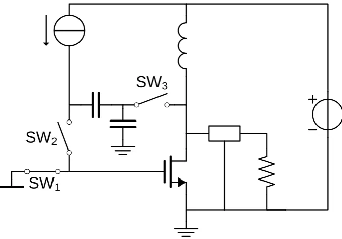
An output filter is added to the design, which is required to increase the performance; mainly efficiency. Also a buffer for the switching signal is required. With these components included the complete top level design is known.
L
chokeZ
AntennaC
injectI
inV
auxZ
MatchingThreshold voltage buffer Switch buffer
Figure 3-11: Complete design of the PA and upconverter combination
23
4
Design
The design of the power amplifier consists of several sub-designs, determined in chapter 3. The schematic is shown below.
The different parts that are required follow from this schematic. First there is the amplifying transistor, the core of the design. The switches and injection capacitor take care of the actual steering. The current source is the input, together with the switch signals that need to be buffered. Also the threshold voltage requires a buffer. The output is connected via a load network. All these are designed and discussed in this chapter.
L
chokeZ
AntennaC
injectI
inV
auxZ
MatchingThreshold voltage buffer Switch buffer
Figure 4-1: Complete design of the PA and upconverter combination
The amplifier is designed for a carrier frequency of 1GHz. This value has been chosen as a reasonable frequency, since it is not designed for a specific application.
4.1
Amplifying transistor
The amplifying transistor needs to be a thick-oxide device to handle the output voltages that can easily become more than 1.2V. To obtain high switching speeds the length should be minimum length, which is 0.28 in our 65nm technology. The total width is set at 4mm, 100x40μm; there is not a specific power that needs to be delivered, so the width is not very important.
24
Table 1: Transistor properties
Threshold voltage ±500mV
Transconductance 450mS
Output impedance 34Ω
Gate-source capacitance 4pF Gate-drain capacitance 2pF Drain-source capacitance 1.6pF
4.1.1 Output impedance
Equation 2-9 gave the output impedance of the circuit depending on transistor properties:
( 4-1 )
This allows us to calculate the output impedance of the circuit given bias conditions. This is done for the used transistor at the previous described operating point.
The injector capacitor needs to be added to , since it is parallel when the transistor is in its on-state. In section 4.2 it is set at 10pF. Entering this in the equation for the output impedance yields:
( 4-2 )
4.2
Injection capacitor
A larger size of the capacitance that is switched between the gate and the drain of the transistor results in more feedback and a more linear gate-drain capacitance. However it also means more current is required at the input, and a larger portion of the feedback goes via switches instead of directly through the intrinsic MOSFET capacitances. This decreases both the efficiency and indirectly also the linearity. Efficiency is obvious, since the larger steering current costs power. The linearity decreases because this current goes via the injection capacitor to the load, and this current contains many harmonics. The amplifier will try to compensate for this due to the feedback, but it will always add harmonics.
The capacitor, , is set at 10pF. This means the gate-drain capacitance becomes the dominant capacitance, and is linearized by the injection capacitor. Going higher than this will not give many benefits.
4.3
Input current source
The input current source steers the amplifier and hence must have a high linearity. As explained in section 0 the amplifier can be seen as a resistor and capacitor parallel from the point of view of the current source. It needs to be able to discharge this capacitor. This means the input source needs to be able to both source and sink current, otherwise discharging can only be done by the exponential RC behavior.
An easy way to get a well defined linear current source is by using a current mirror. This means the baseband input of the circuit is also a current and not a voltage, but since digital to analog converters also normally have a current output, it can be directly connected to the PA.
25 that delivers current from a 1.2V supply. However since the design already requires a 2.5V supply, it might as well be used here also, creating ample of voltage headroom for a current mirror.
A current mirror can only source current and here it also needs to sink current. Adding a current source that sinks current at the output can work, but this always dissipates power from the 2.5V power supply. If an NMOS current mirror to ground is placed, the current source is both able to source current from the 2.5V supply and to sink current to the ground. How much the NMOS mirror sinks depends on their gate voltage, which increases if they need to sink more. Figure 4-2 shows this.
P2
P1
P4
P3
I
in2.5V
N3
N2
N1
Figure 4-2: Complete input current source
Transistors N2 and N3 are able to sink current. This happens if the current from the input source becomes negative. When this happens the cascoded current mirror on top does not need to supply current anymore, resulting in an increase in gate voltage of N2 and N3, forcing them to start conducting. Transistor N1 is used to lower the voltage between the cascoded PMOS current mirror and the input source and the two NMOS transistors
26
4.3.1 Dimensions
The transistors at the left hand side of the current source have a multiplier half of those at the right hand side. So a 2x current gain is present, increasing the efficiency and decreasing the required input power. Larger current gains are possible, but then the linearity is affected, mainly at the fast current changes that include high frequency components, with a larger current gain a smaller input current has to charge all the parasitics.
The two bottom NMOS transistors are long; this gives the required high output impedance. The PMOS transistors can be shorter, since they are cascoded. They need to have a large enough width to provide a sufficiently small input impedance. Transistor N1 is dimensioned to provide the required voltage drop.
Transistors P1 and P3 are 5x20μm/0.1μm, while at the right side they have a two times larger
multiplier, so 10x20μm/0.1μm. This results in an output impedance of 800Ω with a transconductance of 20mS for the right hand side, around their operating point of -600mV gate-source voltage. The cascode structure has a total output impedance of 13kΩ.
Transistor N1 has a size of 10x20μm/0.06μm; with these dimensions it has a voltage drop of 0.5V. N2 and N3 have sizes of respectively 4x5μm/1μm and 8x5μm/1μm. This results in a bias current of 1.2mA combined with an output impedance of 14kΩ for the right hand side of the circuit. Top and bottom combined give an output impedance of the complete current source of 6.7kΩ.
4.3.2 Behavior
Figure 4-3 shows both the actual and the ideal output current for a sinusoid baseband signal. The steering circuit generates a waveform shown by the red ideal line. The simulated output current is very close to the ideal line. The simulated current does include a significant amount of small peaks due to switching in other parts of the amplifier, but since this is at a high frequency and the current is integrated by the injection capacitor this does not have a negative influence on the performance of the PA.
27 One of the main goals of the PA was that it needs to be easy to control. So in the case of a current input, the input impedance needs to be sufficiently low. Figure 4-4 shows the input current and input voltage. From this it follows that the input impedance is a bit under 150Ω. By increasing the
transconductance of the transistors in the mirror this can be decreased further.
Figure 4-4: Input current and input voltage of the current source
28
Figure 4-5: Current through N3 for varying supply voltages
4.4
Auxiliary voltage source
The task of the auxiliary voltage source, shown in Figure 4-1, is to make sure the voltage at the current source is stable, to compensate for its limited output impedance. So ideally this voltage source has a value exactly equal to the output of the amplifier when it is in its on-state. An additional demand is that it may not use special inputs, only the already available input signals can be used. A simple voltage source can be made using a common-source amplifier. This does need to get a steering voltage though, and it is only allowed to use the already available signals, which is a problem. Another problem is that it does need to be able to handle at least a few milli-amperes, which requires a small drain resistor, which means high power consumption.
The alternative is using the output of the PA. This creates the required voltage half the time. A capacitor can store this voltage during the other half, and after this it can be charged to the right voltage again by the PA. Figure 4-6 shows this in the circuit. This also means one switch can be removed, since the capacitor always needs to be connected to the injection capacitor.
When the transistor is in its on-state this capacitor is connected in parallel with the output, so it is charged to exactly the required value. The other half of the cycle it is in series with the injection capacitor. From this it follows that to be a good voltage source this capacitor needs to be significantly larger than the injection capacitor. In principle it is counter-intuitive to put not only an extra
capacitor parallel to the output, but also a very large one. However since it is only parallel one half of the cycle, it will barely affect the output, only the difference in output voltage between two cycles and the charge from the input source needs to be removed from the capacitor every cycle.
29
V
auxFigure 4-6: Auxiliary voltage source in the circuit
4.5
Switches
No switches should be any larger than necessary. Larger switches have more parasitics and higher power consumption than smaller switches. So where possible the switches need to be minimum length.
[image:35.595.75.411.514.749.2]The width of the switches depends mainly on the current that needs to flow through them: when the switches are closed the voltage across them should be low, which requires wide transistors. However to limit parasitics they should not be wider than required for good switching. Depending on the voltage they have to switch they can be implemented using NMOST, PMOST or both.
Figure 4-7 shows the names of the switches, these are used in the design and optimizations in the following sections.
SW
1SW
2SW
330
4.5.1 Switch 1
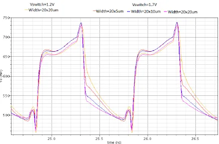
When switch one is closed it will always pull the voltage to a known value, roughly the threshold value. Since this voltage is relative low, an NMOS switch will work much better than a PMOS switch for this. This switch needs to be large enough to force the voltage at the gate quickly to threshold. In figure 4-8 the gate voltage is shown for different widths of the transistor. Also it is shown with a maximum steering voltage of 1.2V and with a maximum of 1.7V. 1.2V is the normal available voltage, however the switching behavior is not good with this voltage. Since the minimum voltage the switch is connected to is 0.5V, and the maximum voltage that is allowed between two terminals is 1.2V, the switching voltage may be up to 1.7V, so it is also simulated with this voltage.
[image:36.595.79.516.269.556.2]From figure 4-8 it is clear that a switch steered with 1.7V is much faster than a switch steered with 1.2V. For this reason it is steered with a voltage switching between 0.5V and 1.7V.
Figure 4-8: Gate voltage as function of the width of switch 1
The used switch is 10 wide with a 20x multiplier, it is clear from the graph that the transistors turns off a bit slower with this width compared to a larger width, but simulations show that this has no negative effect on the performance. Slower is not wanted though, so this width gives a good mix between performance and power consumption.
4.5.2 Switch 2
Switch two has similar requirements as switch 1, in that is also needs to be able to quickly force the gate voltage to a certain value, dictated by the injection capacitor. However since this can be a wide range of values an NMOS alone will not be enough, so a PMOS needs to be parallel, to be able to operate as a good switch over a wide range of voltages.
31 voltage 1.2V above the voltage it switches to, while this switch will have average overdrive voltages of only 0.6V.
Figure 4-9 shows the voltage across the switch as function of its width, with a multiplier of 40, the width of the NMOS and PMOS devices is equal for now.
Figure 4-9: Voltage across switch 2
A width of is used, from these graphs it looks like a smaller width can also be used, but for these simulations switch 3 was ideal. Since switch 3 is in series with switch 2 and will have similar resistance, switch 2 needs to be larger than shown in these simulations to keep the total
on-resistance of switch 2 and 3 combined sufficiently low.
4.5.3 Switch 3
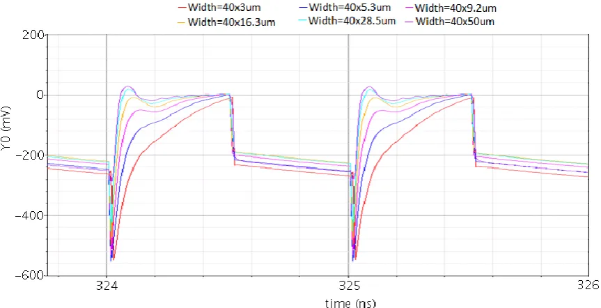
Switch three has a large swing; it needs to be able to short voltages between 0V and 1.2V. This would indicate that an NMOS-PMOS pair is required. However considering the large voltages that can arise at the output, up to 2.5V, high voltage devices are used here. Since from the NMOS the gate voltage will then be switched to 2.5V, an NMOS could also do it without aid from a PMOS. However for reasons explained in section 4.5.4.1 the NMOS-PMOS combination is the best option.
The requirements for the on-resistance are similar to that of switch 2. The transistors will be long instead of that normal transistors are, so they need to be wider for similar behavior. However the higher overdrive voltage lowers again the required width.
32
Figure 4-10: Voltage across switch 4 as function of the width, with an NMOS-PMOS pair
The differences in voltage do not seem to be that large between widely varying widths, however they do propagates directly to the gate, where those differences are significant. The transistors are dimensioned at 40x30μm/0.28μm. Simulations show that this is wide enough for a good linearity. 4.5.4 Charge injection due to switches
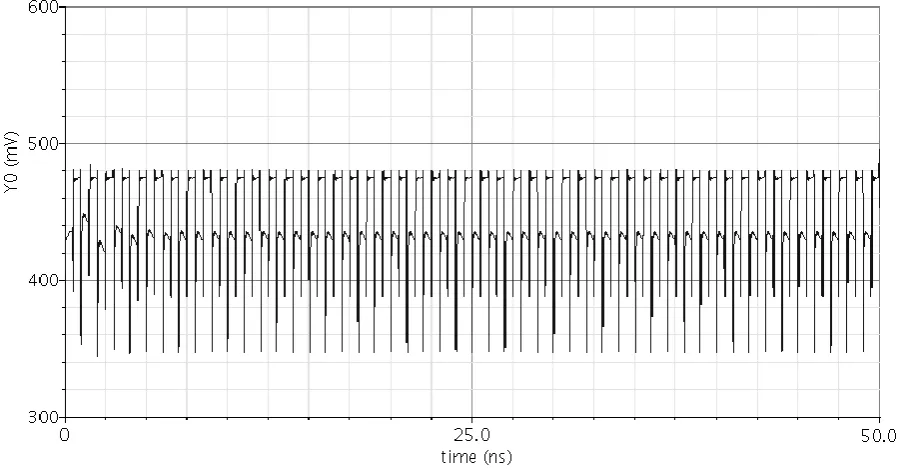
A problem is charge injections due to the switches. Even without a baseband input signal there is an RF output signal. The gate voltage of the amplifying transistor is shown in figure 4-11, the threshold voltage source here was set at a bit lower value than its default 500mV, but this does not affect the injection.
[image:38.595.71.521.487.722.2]33 In the ideal situation the gate voltage should be a flat line. This is important, since now a small input signal would get dominated by the much larger influence of charge injection. This is especially relevant when the input signal has zero-crossings. The phase of the switches will then be inverted, which in combination with the charge injection generates many harmonics.
4.5.4.1 Optimization techniques
A possible solution to counteract the effects of charge injection would be adding a DC current source besides the normal input source that negates the charge injected by the switches. However this would result in two problems: first it will not compensate it exactly, since the switches do not inject a constant current but a train of short peak currents, and secondly because it would be hard to get it at the correct value, independent of process spread.
A good practice is to make the switches as small as possible without influencing the performance for high input signals. This also increases efficiency; however this alone does not give sufficient results. The problem can be solved by injecting an opposite charge at exactly the switching moment, there are two ways to do this [6]; either at both sides of the switching transistor a shorted transistor is of half width is placed that has an inverted control signal, or parallel a PMOS is placed with an inverted control signal. These methods are shown in figure 4-12.
Figure 4-12: Charge injection optimization
The first method is straight forward to implement and does not affect the behavior besides
cancelling the injected charge. The second method does require the PMOS to have the correct width for cancellation, the amount of charge injected depends on the gate-source voltage of the transistor, so equal width is not always the correct solution. However the PMOS does help with conducting, lowering the on-resistance.
4.5.4.2 Optimization
Switch one consists of a single NMOS, so it will inject charge. A PMOS can be placed parallel, however it will barely conduct with the voltage it needs to pull the gate to, 0.5V. To inject a charge similar to that of the NMOS it needs to be wider, since its overdrive voltage will be much lower.
34
Switch two already has an NMOS-PMOS pair. So this can be used to keep the injected charge small. The multiplier of the PMOS is decreased from 40 to 35, which gives for the used operating point a better performance regarding charge injection.
Switch three also has an NMOS-PMOS pair. Their sizes can stay the same; the operating point is such that they cancel each other’s injected charge with equal width. This is also the reason why in the previous section the single NMOS variant was not used, to cancel the injected charge it would require two half width NMOS devices at both sides which would not help conducting, while the PMOS does decrease the on-resistance.
Figure 4-13 shows the gate voltage with the optimization added, which is roughly 18dB better than the non-optimized version.
Figure 4-13: Gate voltage with optimized charge injection
4.6
Switch control voltages
The design has three switches; all three require different voltage levels. The control signals for each switch need to be created and they need to arrive at the same time.
Minimum
Maximum
Switch 1 0.5V 1.7V
Switch 2 0V 1.2V
Switch 3 0V 2.5V
The switch control signals are created from a switch signal that switches between zero and 2.5V. From this the other voltages are made simply by using a thick-oxide inverter that is connected to the minimum and maximum required voltage. After this another inverter is placed for steep edges, since these can be normal thin-oxide devices for all except switch 3 they can be shorter and are faster. The input of the PA will have a normal 1.2V switch signal, so they need to be amplified to 2.5V first. It seems counter-intuitive to first amplify it to 2.5V and then move it back to 1.2V again. However this is done since going from 2.5V to 1.2V is easier to implement than the other way around. So this way the paths for the different switches stay equal as long as possible, decreasing the amount of
35 Ideally all switches would switch at exactly the same time. However since they have different signal paths, with some slower than others, this will not be the case. For this reason there needs to be some headroom, to make sure it cannot happen that switch one can conduct at the same time as one of the other switches.
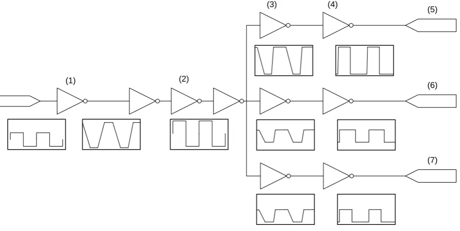
4.6.1 Implementation
The generation of the control signals is shown in figure 4-15. It is shown single ended, but in reality it is a differential.
(5)
(6)
(7)
(1) (2)
[image:41.595.74.527.186.413.2](3) (4)
Figure 4-14: Switch control voltages generation
The input of the system is a 1.2V signal. This is immediately amplified to a 2.5V signal by (1). This is done using a normal common-source stage with resistive load, doing it later would require a smaller resistance to reach the required bandwidth, since the transistor dimensions become larger. A smaller resistance means a larger current goes through the commsource transistors when it is in its on-state, decreasing efficiency.
Now the switch signal is at 2.5V three inverters (3) with increasing widths amplify it to get a good block signal and allow for a larger load. The first inverter also is designed to make sure the duty cycle is 50%; this is not trivial since the flanks of the square wave after (1) are not steep.
36
The resulting switch signals are plotted in figure 4-15; all switches have differential inputs, so the differential signal is plotted. A high signal means the switch closed, so conducting.
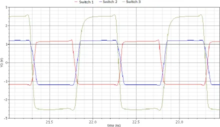
Figure 4-15: Switch control voltages
Switch one starts conducting at the same time when switch two stops conducting, there is very little time between the two. However this does not seem to have a negative effect on the performance. Everywhere else there is plenty of time between opening and closing of switches.
4.7
Output filter
For optimum efficiency an output filter is required. This removes higher harmonics from the output signal and decreases the amount of charge spent on charging and discharging capacitors.
A class E filter is used, this can achieve good efficiency and is used often, its components are shown in figure 4-16.
L
1C
Switch
RFL
L
0C
0 [image:42.595.78.519.112.366.2]R
L37 The most important characteristic of a class E filter in regards to the efficiency is its drain voltage waveform, shown in figure 4-17. When the amplifying transistor is conducting the output voltage is determined by the circuit. When the switch is in the open position the voltage will behave as a damped sine wave. It is dimensioned such that when the PA starts to conduct again, which happens at T=1 in figure 4-17, the voltage across the transistor is again at the same value it was during the last on-state. This way the amplifier does not need spend energy charging/discharging its parasitics every cycle.
Figure 4-17: Normalized class-E waveform for one period
Inductor from figure 4-16 is a choke; it acts as current source and allows the voltage to increase above the power supply voltage. A significant part of the capacitance of capacitor C will come from the parasitic of the amplifier. and are a series resonance circuit tuned to , which is
. They make sure only the required harmonics pass to the load. Larger impedances of and provide better filtering, but also require a larger inductor.
38
L
1C
Switch
RFL
L
0C
0R
L [image:44.595.71.471.71.316.2]V
envelopeFigure 4-18: Class E output filter including ideal equivalent output circuit of the designed amplifier
4.7.1 Inductors
High quality inductors are required for good performance. There are three possible options for inductors: on-chip, off-chip and bond wires.
Using on-chip inductors is a preferable option, since it means no off-chip elements are required. However at a frequency of 1GHz the inductors have a quality factor of only roughly 5-10. Simulations show that mainly efficiency degrades with a lower quality factor, so it is not preferred. It also costs a lot of chip area.
Off-chip inductors can have a very high quality factor, where the series resistance is truly negligible. However they are expensive and a one-chip solution is preferred.
While not primarily intended as inductors, bond wires do have a significant inductance and a low series resistance, so they are suitable as inductors. As rule of thumb they have an inductance of 1nH per mm combined with a series resistance of 0.125Ω per mm. This results at 1GHz in a quality factor of 50. Normal length will be from less than a mm up to a few mm, so inductors between roughly 0.5nH and 5nH can be created using bond wires. They do not require any off-chip components, and they are required anyway, so they are cheap. The main disadvantage is the range of possible inductances and a relative wide spread in their
inductance.
Bond wires are the best option here. The spread in the choke coil will not be a problem, but in the series resonance tank it might be a problem, however this inductor is usually implemented off-chip. A bond wire for the choke coil is easy to implement, since it goes off-chip anyway. It only needs to be of the correct length.
However new techniques might result in future devices having no bond wires, so simulations are done for a quality factor of 10 for on-chip, 30 for bond wires and nearly infinite for off-chip.
4.7.2 Component values
39 The series tank has to suppress higher harmonics, both to help against unwanted radiation and for better class E behavior. A larger inductor gives a better suppression of the harmonics, but requires more space and has a larger parasitic series resistance. Figure 4-19 shows the 2nd and 3rd order harmonics with a 15Ω load as function of different inductor values.
Figure 4-19: Harmonic suppression as function of inductor
[image:45.595.101.486.154.463.2]Second order harmonics should be small compared to 3rd order harmonics, since they do not exist with a 50% duty cycle. An inductor of 10nH is used, the other values that were determined using the equations from [7] are:
Table 2: Output filter
1.4nH 10nH 4.7nH 3pF 2.5pF 15Ω
4.8
Threshold voltage source
The last component from figure 4-1 that needs to be implemented is a buffer that keeps the threshold voltage at the required level. This buffer only needs to sink current that comes from the parasitics of the main capacitor when it is discharged to threshold. Ideally it stays exactly at the threshold voltage, but this is not realistic and simulations indicated that variations of a few tens of millivolts are acceptable.
10-9 10-8 10-7
40
To do this an NMOS transistor can sink the current, while a capacitor parallel removes the current peaks. The NMOS is controlled by an OpAmp with feedback from the drain of the NMOS, so where should be the threshold voltage.
The OpAmp is created with a very basic differential input pair combined with a common-source PMOS amplifier. No compensation capacitors are present: the output, the NMOS, is a current source into a mainly capacitive load. This is the dominant pole in the system, so no other one should be added.
[image:46.595.76.455.209.448.2]The circuit is shown in figure 4-20.
Figure 4-20: Threshold voltage source
The OpAmp is most likely not the best possible design. It is more a proof-of-concept that it works. Transistors N1 and N2 have dimensions of 3x5μm/0.06μm, while P1 and P2 have 2x1μm/0.06μm. P3 is 50% larger than that with 3x1μm/0.06μm. R is 4kΩ and N3 is 10x10μm/0.06μm.
The capacitor needs to be large for correct circuit behavior, since it needs to absorb the current peaks produced by the switching of the amplifier. Large capacitors are also expensive, so it should not be larger than absolutely necessary.
41 Figure 4-21: Threshold voltage with different capacitances
43
5
Simulation results
Simulations of the designed amplifier are discussed in this chapter. First the two most important results are discussed, those regarding the linearity and the efficiency. After that the effects of different quality factors of the choke, variation in the threshold voltage source and width-scaling of the amplifier on the performance of the amplifier are simulated and discussed.
Unless otherwise noted a quality factor of 30 is assumed for the choke. Another quality factor has mainly influence on the efficiency, and only a small influence on the linearity; a lower quality factor results in a bit higher impedance seen by the amplifying transistor due to the extra resistance in series with the choke.
The MOSFETs are TSMCs CLN65 devices. All other components, except the choke, are assumed ideal. The switch frequency is set at 1GHz for all the simulations.
5.1
Linearity
Linearity is both assessed using single tone outputs to find the 1dB compression point and two-tone outputs to find the intermodulation behavior.
5.1.1 1dB compression point
The 1dB compression point is simulated using a 1GHz output signal with increasing amplitude, created by using a DC current input. Since the designed system is both amplifier and upconverter, this results with a 1GHz switch signal in a 1GHz RF output. Figure 5-1 shows the resulting output power, the Q-factor of the choke coil was 30. Here a difference in Q-factor only results in a small vertical shift, but has no significant influence on the shape.
[image:49.595.79.506.461.701.2]The vertical axis shows the output power of the 1GHz tone in dBm, while the horizontal axis is related to the logarithm of the input current, but does not directly represent a power. This result contains three interesting parts, low power, medium power and high output power.
Figure 5-1: Single tone output power with increasing input power
44
[image:50.595.80.506.138.375.2]In the center region the output rises slightly faster than what should happen in the linear case. This happens due to the increasing gain at higher outputs, the feedback is not sufficient to completely eliminate this. Since both axes are logarithmic the linear line cannot have a different steepness to fit better.
Figure 5-2: Single tone output power with ideal linear curve
This makes calculating the 1dB compression point from this curve tricky; generally the extrapolation can be started from a low input power, however in this case starting a low input power means the -1dB line is several dBs below the actual output power when the amplifier starts to saturate. However since the amplifier quickly goes from normal operation to clipping it does not matter a lot for the output referred 1dB compression point, the curve is almost flat at the 1dB compression point. Extrapolated from an input of 10dB, the output referred 1dB compression is 16.9dBm, while when it is extrapolated from an input of 0 dB it is equal to 17.4dBm. The maximum reached output power is 17.5dBm, with a theoretical limit of 21.9dBm if an ideal square wave with an amplitude of 1.2V was present.
The final interesting area of this graph is where the input power is high; if the input power continues to increase the output power starts to decrease. This happens because the amplifier gets
45 Figure 5-3: Gate voltage in normal operating region and when oversteered
At 15dB input the gate voltage is as expected, it has some issues pulling the gate to threshold while due to the input current the gate voltage increases in its on-state.
However with 30dB input the gate voltage reaches far too high voltages. The cause is a combination of too high input currents and the non-ideal switch that has to pull the gate voltage to threshold combined with the non-ideal threshold source. The high input current causes it to reach high
voltages. At this point the amplifier is not capable anymore of pulling the gate to threshold. Since the gate does not reach threshold the capacitances of the amplifying transistor are not sufficiently far discharged, and the next cycle it reaches even higher voltages. This continues until periodic steady state is achieved.
5.1.2 Intermodulation distortion
46
Figure 5-4: Two-tone test with 10MHz input
47 Figure 5-5: Difference between first order response and worst IMD3 product
The difference between the IMD products is because to the input current that flows through the injection capacitor also being mixed up. This also results in a noticeable, but much smaller, difference between the two first order responses. With a lower baseband frequency this problem becomes smaller, shown in figure 5-6.
[image:53.595.78.514.458.733.2]48
5.2
Efficiency
[image:54.595.65.530.530.738.2]The efficiency depends on the output power delivered. A higher power means a higher efficiency, since most of the power consumption in the amplifier will be largely independent of the output power delivered. Figure 5-7 shows the efficiency and total power consumption versus the output power.
Figure 5-7: Efficiency as function of the output power
5.2.1 Power consumption per component
At a DC input of 15dB, which means the amplifier’s output is 1GHz with maximum amplitude, the distribution of the power consumption is as follow:
Table 3: Power distribution of amplifier at maximum output
Component Power consumption Percentage
Total 225.4mW 100%
Amplifier 177.9mW 78.9%
Input current source 26.7mW 11.8%
Switch control 100.6mW 44.6%
Initial amplification 37.4mW 16.5%
Switch 1 6.9mW 3.1%
Switch 2 5.2mW 2.3%
Switch 3 51.1mW 22.7%
Threshold source 0.45mW 0.2%
Output stage (minus load) 50.1mW 22.2%
Load 47.5mW 21.1%
1.2V rail 99.7mW 44.2%
2.5V rail 125.6mW 55.7%
0 50 100 150 200 250 0% 5% 10% 15% 20% 25%
0 10 20 30 40 50
To ta l p o w er c o n su mption ( mW) Effi ci en cy
Output power (mW)
49 With no input, the power distribution is:
Table 4: Power distribution of amplifier with no input
Component Power consumption Percentage
Total 109.1mW 100%
Amplifier 109.1mW 100%
Input current source 4.6mW 4.2%
Switch control 99.2mW 90.9%
Initial amplification 37.4mW 34.3%
Switch 1 7mW 6.4%
Switch 2 5.1mW 4.7%
Switch 3 49.8mW 45.6%
Threshold source 0.44mW 0.4%
Output stage (minus load) 4.9mW 4.5%
Load 7.6μW 0%