Resetting Asynchronous QDI Systems
Thesis by
Xiaofei Chang
In Partial Fulfillment of the Requirements for the Degree of
Master of Science
California Institute of Technology Pasadena, California
c
2013
Acknowledgements
Abstract
Contents
1 Introduction 1
2 GRS 3
2.1 Operation Protocol . . . 3
2.2 Pipelines . . . 5
2.2.1 Pipelines with Split Control and Datapath for GRS . . 5
2.2.1.1 Control Logic . . . 6
2.2.1.2 Register . . . 8
2.2.1.3 Function Block . . . 9
2.2.1.4 Complete Pipeline Stage . . . 10
2.2.2 Fine-Grain Integrated Pipelines for GRS . . . 10
2.2.2.1 WCHB Dual-Rail Buffer for GRS . . . 10
2.2.2.2 PCHB Dual-Rail Buffer for GRS . . . 11
2.2.2.3 PCFB Dual-Rail Buffer for GRS . . . 13
3 WRS 15 3.1 Operation Protocol . . . 15
3.2 Pipelines . . . 16
3.2.1 Pipelines with Split Control and Datapath for WRS . . 16
3.2.1.1 Control Logic . . . 17
3.2.1.2 Register . . . 18
3.2.1.3 Function Block . . . 19
3.2.1.4 Complete Pipeline Stage . . . 20
3.2.2 Fine-Grain Integrated Pipelines for WRS . . . 21
3.2.2.1 WCHB Dual-Rail Buffer for WRS . . . 21
3.2.2.2 WCHB 1-of-4 Buffer for WRS . . . 23
3.2.2.3 PCHB Dual-Rail Buffers . . . 25
3.2.2.4 PCFB Dual-Rail Buffers . . . 25
3.2.2.5 Buffers with Logic . . . 26
3.3 Special Blocks . . . 31
3.3.1 Source/Sink . . . 31
3.3.2 Initial Buffer . . . 32
3.3.3 Channel Arbiter . . . 33
3.3.4 Slack Zero Process . . . 35
4 Global Reset Insertion 38 4.1 Breadth First Search (BFS) . . . 39
4.2.1 Pseudocode . . . 40
4.2.2 Proof of Correctness . . . 40
4.2.2.1 Initialization . . . 40
4.2.2.2 Maintenance . . . 40
4.2.2.3 Termination . . . 41
5 Iterative Multiplier 43 5.1 Iterative Multiplier . . . 43
5.2 Simulation . . . 44
6 Conclusion 48
List of Figures
1 Pipeline Stage with Split Control and Datapath for GRS . . . 6
2 Control Logic for GRS . . . 7
3 Completion Tree . . . 8
4 Register for GRS . . . 8
5 Input Enable Generator for GRS . . . 9
6 Function Block for GRS . . . 9
7 WCHB Dual-Rail Buffer for GRS . . . 11
8 PCHB Dual-Rail Buffer for GRS . . . 12
9 Reset Gate for C-element . . . 12
10 PCFB Dual-Rail Buffer for GRS . . . 13
11 Process with LRG for WRS . . . 16
12 Pipeline Stage with Split Control and Datapath for WRS . . . 17
13 Control Logic for WRS . . . 18
14 Register for WRS . . . 19
15 Input Enable Generator for WRS . . . 19
16 Function Block for WRS . . . 20
17 WCHB Dual-Rail Buffer for WRS 1 . . . 22
18 WCHB Dual-Rail Buffer for WRS 2 . . . 23
19 WCHB 1-of-4 Buffer for WRS . . . 24
20 PCHB Dual-Rail Buffer for WRS . . . 25
21 PCFB Dual-Rail Buffer for WRS . . . 26
22 Source for WRS . . . 31
23 Sink for WRS . . . 31
24 Initial Buffer for WRS . . . 32
25 Channel Arbiter . . . 33
26 Basic Arbiter . . . 34
27 Channel Arbiter for WRS . . . 35
28 Pseudocode of Breadth First Search (BFS) . . . 40
29 Pseudocode of BFS with Multiple Roots . . . 41
30 Iterative Multiplier . . . 43
31 Reset Time for Different Process Corners . . . 45
32 Cycle Time for Different Process Corners . . . 46
List of Tables
1 Dual-Rail Data Codes . . . 4
2 1-of-4 Data Codes . . . 4
3 Dual-Rail Data Codes for WRS . . . 15
1
Introduction
Asynchronous systems with the only delay assumption of isochronic forks are called Quasi Delay-Insensitive (QDI) systems [1]. QDI systems are com-posed of concurrent modules called processes. Processes communicate with each other by sending and receiving actions on channels. Each channel is comprised of one or several directed data wires and one directed enable wire. Data wires from a sender process to a receiver process encode the message being sent while the enable wire from a receiver process to a sender process is used to notify the sender process that the message has been received.
During normal operation, communication between processes occurs con-currently with computation inside each process. However, in order for a QDI system to transit into normal operation after power-on, it needs to be driven into the valid initial state that is determined by Martin’s synthesis. The procedure that brings a system into its valid initial state after power-on is called reset. The valid initial state of a QDI system is determined by the valid initial state of each process in the system. The valid initial state of a process is determined by valid initial values of all wires inside the process. Therefore each wire in the system needs to be driven to the valid initial value before normal operation of the system starts.
values.
2
GRS
For a given process P, the initial value of any input wire I is determined by the gate inside the neighboring process that drives I. Initial values of internal wires and output wires are determined by gates inside P that drive them. If initial values of input wires and corresponding gates can drive all internal wires and output wires to the valid initial values, P will be reset to the valid initial state once neighboring processes have been reset to the valid initial states. Otherwise, reset logic needs to be added in order to force internal wires and output wires to assume valid initial values.
Added reset logic converts logic gates into reset gates. Each reset gate has an extra input that is connected to GR. When GR is asserted, the output of a reset gate is driven to the valid initial value independent of the other inputs. If all logic gates in a QDI system are converted into reset gates, the system is guaranteed to be in the valid initial state because GR forces each wire to assume the valid initial value. However, converting all logic gates into reset gates slow down normal operation of the system because reset gates are slower than corresponding logic gates. Therefore, only necessary logic gates should be converted into reset gates. To be more specific, only logic gates that can’t drive their outputs to valid initial values based on valid initial values of inputs should be converted into reset gates. Once there are enough reset gates, each wire will be driven to the valid initial value when GR is asserted and the system will be driven to the valid initial state. After reset phase, GR is deasserted and normal operation starts. Reset gates function in the same way as the original logic gates during normal operation.
2.1
Operation Protocol
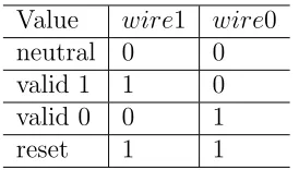
Delay-Insensitive (DI) codes are used in QDI systems for data communica-tion. DI codes encode validity and neutrality of data within the data itself. There are many DI codes, among which dual-rail codes and 1-of-n codes are normally used. Each wire in dual-rail codes or 1-of-n codes is used for one value of the data. When all wires are 0s, the data is neutral. When one of the wires is 1, the data is valid. For example, dual-rail codes are shown in Table 1. When (wire1, wire0) = (0,0), data is neutral. When (wire0, wire1) = (0,1) or (wire0, wire1) = (1,0), data is valid 1 or valid 0. The rest combination of values ((wire1, wire0) = (1,1)) is invalid.
Value wire1 wire0
neutral 0 0
valid 1 1 0
valid 0 0 1
Table 1: Dual-Rail Data Codes
Value wire3 wire2 wire1 wire0
neutral 0 0 0 0
valid 3 1 0 0 0
valid 2 0 1 0 0
valid 1 0 0 1 0
valid 0 0 0 0 1
Table 2: 1-of-4 Data Codes
Besides data wires encoded as 1-of-n, each channel contains another
enable wire. Data wires from a sender process to a receiver process en-code the message being sent while the enable wire is used by the receiver process to notify the sender process that the message has been received. The communication protocol between a sender process and a receiver process is shown in (1), where v() and n() are validity and neutrality tests.
sender: data↑; [¬enable]; data↓; [enable]
receiver: [v(data)]; enable↓; [n(data)]; enable↑ (1)
2.2
Pipelines
In order to increase throughput, computation is pipelined. Each process forms a pipeline stage. Most pipeline stages repeat actions of receiving data from inputs, computing functions of data and sending results through out-puts as described by CHP in (2), where I0, I1, ...In−1, O0, O1, ..., Om−1 and
f0(X), f1(X), ..., fm(X) are respectively inputs, outputs and functions while
X refers to the set of variables {x0, x1, ..., xn−1}. Because they share similar
communication sequences, they can be implemented with templates. There are two types of templates to implement pipeline stages: pipelines with split control and data and fine-grain integrated pipelines.
∗[I0?x0, I1?x1, ..., In−1?xn−1;O0!f0(X), O1!f1(X), ..., Om−1!fm−1(X)] (2)
2.2.1 Pipelines with Split Control and Datapath for GRS
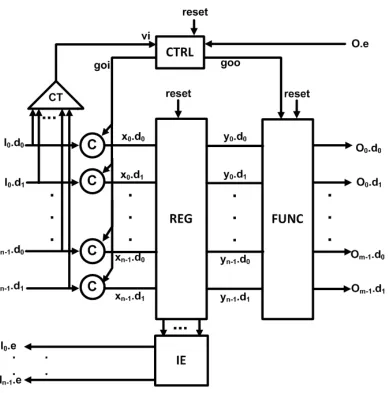
Figure 1: Pipeline Stage with Split Control and Datapath for GRS
2.2.1.1 Control Logic The expected state transition of CTRL is de-scribed by HSE as shown in (3). CTRL first enables REG to receive data from inputs (goi↑). Once data has been latched by REG ([(x0∧y0)∨(x1∧y1)]),
CTRL acknowledges the input (I.e ↓). It then enables FUNC to compute functions on received data and output computed results (goo↑). Other state-ments in (3) are used to complete four-phase handshake protocol.
∗[[vi];goi↑; [¬vi];goi↓;goo↑; [¬O.e];goo↓; [O.e]] (3)
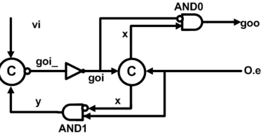
Figure 2: Control Logic for GRS
[¬reset]; [¬vi],[¬O.e], reset ↑; (y ↓);goi ↑;goi↓;x↓;goo↓; [reset]; [O.e];
∗[[vi], y ↑;goi ↓;goi↑; (x↑;y↓);
[¬vi];goi ↑;goi ↓;goo↑; [¬O.e];x↓;goo↓; [O.e]]
(4)
If the internal variables are removed, (4) is simplified to (5).
[¬reset]; [¬vi],[¬O.e], reset ↑;goi↓;goo↓; [reset]; [O.e];
∗[[vi];goi ↑; [¬vi];goi ↓;goo↑; [¬O.e];goo↓; [O.e]]
(5)
The nonterminating repetition part inside ∗[ ] of (5) implements the ex-pected transition in (3). Therefore, the circuit implementation is correct.
Figure 3: Completion Tree
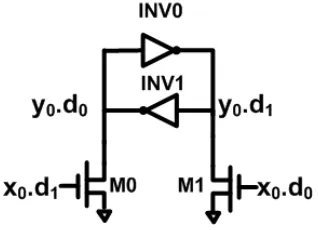
2.2.1.2 Register REG is comprised of n 1-bit registers. The 1-bit regis-ter is implemented as shown in Figure 4. During reset phase, (x0.d0, x0.d1) =
(0,0). M0 and M1 are cut off. The cross-coupled inverters may enter the metastable state. However, the probability that the metastable state re-tains through the whole reset phase is negligible. Therefore, before normal operation starts, (y0.d0.y0.d1) = (0,1) or (y0.d0.y0.d1) = (1,0).
Figure 4: Register for GRS
During normal operation, if (x0, x1) is neutral, (y0, y1) retains the previous
data. If (x0, x1) is valid, it is latched into (y0, y1).
TheIE block in Figure 1 is used to generateenable signals for all inputs. It contains ncopies of circuits shown in Figure 5. During reset phase,enable
[image:16.612.226.385.434.549.2]Figure 5: Input Enable Generator for GRS
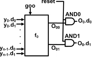
2.2.1.3 Function Block FUNC containsmcopies of circuit blocks shown in Figure 6 to generate m different outputs. f0 can be any combinational
logic function with inputs of gooand (y0.d0, y0.d1) to (yn−1.d0, yn−1.d1). The
state transition of the circuit block is described in (6).
Figure 6: Function Block for GRS
([¬reset];O0.d0 ↓, O0.d1 ↓),
([¬goo];O00↓, O01 ↓),([(y0.d0 xory0.d1)∧...∧(yn−1.d0 xoryn−1.d1)]);
[reset];
∗[[goo∧f01(y0.d0, y0.d1, ..., yn−1.d0, yn−1.d1)→O00 ↓, O01↑;O0.d0 ↓, O0.d1 ↑
[]goo∧f00(y0.d0, y0.d1, ..., yn−1.d0, yn−1.d1)→O01↓, O00↑;O0.d1 ↓, O0.d0 ↑
[¬r];O00 ↓, O01↓;O0.d0 ↓, O0.d1 ↓]
(6) During reset phase, (O0.d0, O0.d1) = (0,0). During normal operation, the
[image:17.612.228.387.384.480.2]2.2.1.4 Complete Pipeline Stage The state transition of the whole pipeline stage shown in Figure 1 is described by HSE in (7). During reset phase, all inputs and outputs are neutral and all enable signals are driven to 0s. During normal operation, alternating valid and neutral data comes from the inputs and corresponding alternating valid and neutral data is gen-erated at the outputs. Therefore the implementation is consistent with GRS operation protocol.
[¬reset]; [n(I0)∧...∧n(In−1)],
(O0.d0 ↓, O0.d1 ↓, ..., Om−1.d0 ↓, Om−1.d1 ↓),
I0.e↓, ..., In−1.e↓,[¬O0.e∧...∧ ¬Om−1.e];
vi↓;goi↓;goo↓, x0.d0 ↓, x0.d1 ↓, ..., xn−1.d0 ↓, xn−1.d1 ↓;
[reset];I0.e↑, ..., In−1.e↑,[O0.e∧...∧Om−1.e];
∗[[v(I0)∧...∧v(In−1)];vi↑;goi↑;
[I0.d0 →x0.d0 ↑;y0.d0 ↑[]I0.d1 →x0.d1 ↑;y0.d1 ↑],
...,
[In−1.d0 →xn−1.d0 ↑;yn−1.d0 ↑[]In−1.d1 →xn−1.d1 ↑;yn−1.d1 ↑];
I0.e↓, ..., In−1.e↓; [n(I0)∧...∧n(In−1)];vi↓;goi↓;
x0.d0 ↓, x0.d1 ↓, ..., xn−1.d0 ↓, xn−1.d1 ↓;I0.e↑, ..., In−1.e↑;goo↑;
[f00(y0.d0, y0.d1, ..., yn−1.d0, yn−1.d1)→O0.d0 ↑
[]f01(y0.d0, y0.d1, ..., yn−1.d0, yn−1.d1)→O0.d1 ↑],
...,
[f(m−1)0(y0.d0, y0.d1, ..., yn−1.d0, yn−1.d1)→Om−1.d0 ↑
[]f(m−1)1(y0.d0, y0.d1, ..., yn−1.d0, yn−1.d1)→Om−1.d1 ↑];
[¬O0.e∧...∧ ¬Om−1.e];goo↓;
O0.d0 ↓, O0.d1 ↓, ..., Om−1.d0 ↓, Om−1.d1 ↓; [O0.e∧...∧Om−1.e]]
(7)
2.2.2 Fine-Grain Integrated Pipelines for GRS
In the second approach, control logic and datapath are integrated into a single component. Three commonly used templates, namely Weak-Conditioned Half Buffers (WCHB), Precharged Half Buffers (PCHB) and Precharged Full Buffers (PCFB) [3], are modified to adapt to GRS.
[¬reset];I.e↓,[¬O.e∧ ¬I.d0 ∧ ¬I.d1];O.d0 ↓, O.d1 ↓;
[reset];I.e↑;
∗[[I.d0∧O.e→O.d0 ↑[]I.d1∧O.e→O.d1 ↑];I.e− ↓
[¬I.d0∧ ¬I.d1∧ ¬O.e];O.d0−, O.d1−;I.e+]
(8)
Figure 7: WCHB Dual-Rail Buffer for GRS
reset(0) indicates that once the active-lowreset is asserted,I.e is driven to 0 independent of O.d0 and O.d1. The neighboring processes should
fol-low the same operation protocol. O.e is driven to 0 during reset phase. In addition, (I.d0, I.d1) = (0,0) because the outputs of IP are reset to
neu-tral value during reset phase. Both inputs to the C-elements are 0s and (O.d0, O.d1) = (0,0). The neutral data from IP propagates to NIP and
gen-erates neutral data at outputs of NIP. The neutral data further propagates to other NIP until all processes have output neutral data.
Once reset is deasserted, I.e is driven to 1 since (O.d0, O.d1) = (0,0).
O.e from the neighboring process is driven to 1 as well. Once valid data arrives at (I.d0, I.d1), it will be propagated to (O.d0, O.d1). The behavior of
the implementation is consistent with the operation protocol of GRS.
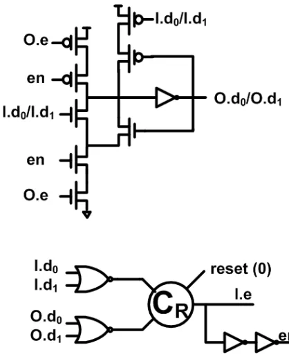
2.2.2.2 PCHB Dual-Rail Buffer for GRS PCHB dual-rail buffer for GRS is described in (9) and implemented as shown in Figure 8.
[¬reset];I.e↓, en↓,[¬O.e];O.d0 ↓, O.d1 ↓,[¬I.d0∧ ¬I.d1];
[reset];I.e↑;
∗[[I.d0∧O.e→O.d0 ↑[]I.d1∧O.e→O.d1 ↑];I.e↓;
[¬O.e];O.d0 ↓, O.d1 ↓; [¬I.d0∧ ¬I.d1];I.e↑]
Figure 8: PCHB Dual-Rail Buffer for GRS
CR is the reset gate for a normal C-element. Depending on whether the initial value is 0 or 1, it is implemented as shown in Figure 9.
Figure 9: Reset Gate for C-element
[image:20.612.169.441.463.652.2]processes should follow the same operation protocol. O.eis driven to 0 during reset phase. Therefore O.d0 and O.d1 are driven to 0s. Similarly, the output
of the previous stage should be driven to (0,0), i.e., (I.d0, I.d1) = (0,0).
Onceresetis deasserted,I.eis driven to 1 as well asensince (I.d0, I.d1) =
(0,0) and (O.d0, O.d1) = (0,0). Similarly, O.e from the neighboring process
is driven to 1. Once valid data arrives at (I.d0, I.d1), it will be propagated
to (O.d0, O.d1). The behavior of the implementation is consistent with the
operation protocol of GRS.
2.2.2.3 PCFB Dual-Rail Buffer for GRS PCFB dual-rail buffer for GRS is described in (10) and implemented as shown in Figure 10.
[¬reset];I.e↓, x↓,[¬O.e];O.d0 ↓, O.d1 ↓,[¬I.d0∧ ¬I.d1];
[reset];I.e↑, x↑;
∗[[I.d0∧O.e→O.d0 ↑[]I.d1∧O.e→O.d1 ↑];I.e↓;x↓
[¬O.e];O.d0−, O.d1−; [¬I.d0∧ ¬I.d1];I.e↑;x↑]
[image:21.612.172.440.346.599.2](10)
Figure 10: PCFB Dual-Rail Buffer for GRS
C0 is an asymmetrical C-element. It is implemented as described by Production Rule Set (PRS) in (11).
¬reset∨(vi∧x∧vo)→I.e↓
When reset is asserted, I.e is driven to 0 as well as the internal variable
x. The neighboring processes should follow the same operation protocol.
O.e is driven to 0 during reset phase. Therefore, (O.d0 , O.d1 ) = (1,1) and
(O.d0, O.d1) = (0,0). Similarly, the output of the previous stage should be
driven to (0,0), i.e., (I.d0, I.d1) = (0,0).
Onceresetis deasserted,I.e is driven to 1 as well as the internal variable
x. Similarly, O.efrom the neighboring process is driven to 1. Once valid data arrives at (I.d0, I.d1), it will be propagated to (O.d0, O.d1). The behavior of
3
WRS
For WRS, the Global Reset (GR) is connected to Initial Processes (IP). Once GR is asserted, IP will output reset data that is data with reset value. Reset value is the third possible value besides neutral and valid values for given data codes. Reset data propagates and triggers the Local Reset Generator (LRG) of each process. LRG asserts the Local Reset (LR) and forces the process to output reset data. This propagation of reset data continues until all processes have been reset. After that, GR is deasserted and neutral data will be generated from IP. Neutral data propagates and overwrites all reset data. In addition, LRG can’t be triggered by neutral or valid data and no reset data will be generated. The system will operate normally with only neutral and valid data.
3.1
Operation Protocol
In order to include the third possible value - reset value, both dual-rail codes and 1-of-n codes need to be modified. For the modified dual-rail codes, the rest value (wire1, wire0) = (1,1) is used to be the reset value. For the modified 1-of-n (n ≥ 3) codes, reset value is defined as two wires being 1s while the rest wires being 0s. Reset value is chosen in this way to make implementation of LRG simple. For example, modified dual-rail codes and 1-of-4 codes for WRS are respectively shown in Table 3 and Table 4.
Value wire1 wire0
neutral 0 0
valid 1 1 0
valid 0 0 1
[image:23.612.238.375.466.544.2]reset 1 1
Table 3: Dual-Rail Data Codes for WRS
Value wire3 wire2 wire1 wire0
neutral 0 0 0 0
valid 3 1 0 0 0
valid 2 0 1 0 0
valid 1 0 0 1 0
valid 0 0 0 0 1
reset 0 0 1 1
Table 4: 1-of-4 Data Codes for WRS
Figure 11: Process with LRG for WRS
After that, GR is deasserted and IP will output alternating neutral and valid data. Neutral data propagates and overwrites all reset data. Besides, no new reset data will be generated since LRG will not be triggered by neutral or valid data. From then on, the system has only neutral and valid data propagating inside. Therefore, processes in the system with WRS follow the operation protocol of receiving and generating reset data followed by receiving and generating alternating neutral and valid data.
3.2
Pipelines
As in QDI systems with GRS, there are two approaches to implement pipelines in QDI systems with WRS. However, templates need to be modified in order to accommodate the extra reset value in dual-rail or 1-of-n codes for WRS.
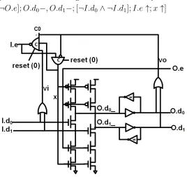
3.2.1 Pipelines with Split Control and Datapath for WRS
stage still contains three major components: CTRL, REG and FUNC as in Figure 1. The difference is instead of resetting all three blocks with GR, two LR reset0 and reset1 are generated by NAND0 and NAND1. reset0 resets
[image:25.612.112.500.197.551.2]CTRL while reset1 resets REG and FUNC.
Figure 12: Pipeline Stage with Split Control and Datapath for WRS
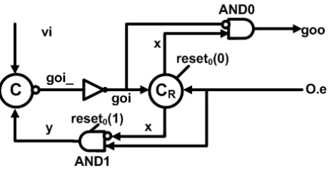
3.2.1.1 Control Logic The circuit implementation of CTRL is shown in Figure 13. The state transition of the circuit is described by HSE in (12).
[¬reset0]; [vi],[¬O.e], x↓, y ↑;goi ↓;goi↑;goo↓;
[reset0];y↓; [¬vi];goi ↑;goi ↓; [O.e];
∗[[vi], y ↑;goi ↓;goi↑;x↑;y↓;
[¬vi];goi ↑;goi ↓;goo↑; [¬O.e];x↓;goo↓; [O.e]]
Figure 13: Control Logic for WRS
If the internal variables are removed, (12) is simplified to (13).
[¬reset0]; [vi∧ ¬O.e];goi↑;goo↓;
[reset0]; [¬vi∧O.e];goi↓;
∗[[vi];goi ↑; [¬vi];goi ↓;goo↑; [¬O.e];goo↓; [O.e]]
(13)
For the nonterminating repetition part inside ∗[ ], channels L and R respectively implement the expected transition in (3). Therefore, the circuit implementation is correct.
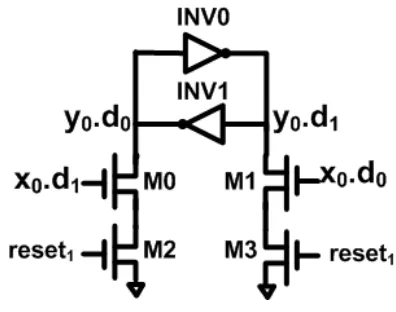
3.2.1.2 Register The implementation of REG shown in Figure 4 is not suitable for WRS. During reset phase of WRS, bothx0.d0andx0.d1are driven
to 1s and M1 and M0 are closed. Direct conducting path between VDD and GND forms through INV0 and M1 or through INV1 and M0. Therefore REG is modified as shown in Figure 14. During reset phase, reset1 is 0 and
both M2 and M3 are cut off. Therefore, no direct conducting path between VDD and GND is formed. During normal operation, reset1 is always 1 and
Figure 14: Register for WRS
TheIE block in Figure 12 is used to generateenablesignals for all inputs. It contains n copies of circuits shown in Figure 15. During reset phase,x0.d0
and x0.d1 are driven to 1s. y0.d0 andy0.d1 are complementary. I0.e is driven
to 0 as well as all otherenablesignals for inputs. No resetsignal needs to be inserted. During normal operation, if the input is neutral, the enable signal is driven to 1. If the input is valid and latched by the register, the enable signal is driven to 0.
Figure 15: Input Enable Generator for WRS
3.2.1.3 Function Block FUNC containsmcopies of circuit blocks shown in Figure 16 to generate m different outputs. f0 can be any combinational
logic function with inputs of gooand (y0.d0, y0.d1) to (yn−1.d0, yn−1.d1). The
[image:27.612.227.383.433.583.2]Figure 16: Function Block for WRS
([¬reset1];O0.d0 ↑, O0.d1 ↑),
([¬goo];O00↓, O01 ↓),([(y0.d0 xory0.d1)∧...∧(yn−1.d0 xoryn−1.d1)]);
[reset1];O.d0 ↓, O.d1 ↓;
∗[[goo∧f01(y0.d0, y0.d1, ..., yn−1.d0, yn−1.d1)→O00 ↓, O01↑;O0.d0 ↓, O0.d1 ↑
[]goo∧f00(y0.d0, y0.d1, ..., yn−1.d0, yn−1.d1)→O01↓, O00↑;O0.d1 ↓, O0.d0 ↑
[¬r];O00 ↓, O01↓;O0.d0 ↓, O0.d1 ↓]
(14) When LR reset1 is asserted, reset data is generated at the output
(O.d0 ↑, O.d1 ↑). When reset1 is deasserted and neutral data is generated
at the output. After that, r assumes alternating 1 and 0 and corresponding valid and neutral data is generated at the output.
3.2.1.4 Complete Pipeline Stage The state transition of the whole pipeline stage is described in (15). When reset data arrives at the Local Reset Input input (LRI) ([I0.d0∧I0.d1]), reset data is generated at all outputs
(O0.d0 ↑, O0.d1 ↑, ..., Om−1.d0 ↑, Om−1.d1 ↑). All enable signals are driven to
0s.
[I0.d0∧I0.d1∧...∧In−1.d0∧In−1.d1];reset0 ↓;vi ↑;goi ↑;
goo↓, x0.d0 ↑, x0.d1 ↑, ..., xn−1.d0 ↑, xn−1.d1 ↑;
reset1 ↓; [y0.d1 ↑, y0.d0 ↓[]y0.d0 ↑, y0.d1 ↓], ...,
[yn−1.d1 ↑, yn−1.d0 ↓[]yn−1.d0 ↑, yn−1.d1 ↓],
O0.d0 ↑, O0.d1 ↑, ..., Om−1.d0 ↑, Om−1.d1 ↑;
I0.e↓, ..., In−1.e↓,[¬O0.e∧...∧ ¬Om−1.e];
[¬I.d0∧ ¬I.d1 ∧...∧ ¬In−1.d0 ∧ ¬In−1.d1];
reset0 ↑, vi↓;goi↓;x0.d0 ↓, x0.d1 ↓, ..., xn−1.d0 ↓, xn−1.d1 ↓;
I0.e↑, ..., In−1.e↑;reset1 ↑;
O0.d0 ↓, O0.d1 ↓, ..., Om−1.d0 ↓, Om−1.d1 ↓; [O0.e∧...∧Om−1.e]
∗[[v(I0)∧...∧v(In−1)];vi↑;goi↑;
[I0.d0 →x0.d0 ↑;y0.d0 ↑[]I0.d1 →x0.d1 ↑;y0.d1 ↑],
...,
[In−1.d0 →xn−1.d0 ↑;yn−1.d0 ↑[]In−1.d1 →xn−1.d1 ↑;yn−1.d1 ↑];
I0.e↓, ..., In−1.e↓; [n(I0)∧...∧n(In−1)];vi ↓;goi ↓;
x0.d0 ↓, x0.d1 ↓, ..., xn−1.d0 ↓, xn−1.d1 ↓;I0.e↑, ..., In−1.e↑;goo↑;
[f00(y0.d0, y0.d1, ..., yn−1.d0, yn−1.d1)→O0.d0 ↑
[]f01(y0.d0, y0.d1, ..., yn−1.d0, yn−1.d1)→O0.d1 ↑],
...,
[f(m−1)0(y0.d0, y0.d1, ..., yn−1.d0, yn−1.d1)→Om−1.d0 ↑
[]f(m−1)1(y0.d0, y0.d1, ..., yn−1.d0, yn−1.d1)→Om−1.d1 ↑];
[¬O0.e∧...∧ ¬Om−1.e];goo↓;
O0.d0 ↓, O0.d1 ↓, ..., Om−1.d0 ↓, Om−1.d1 ↓; [O0.e∧...∧Om−1.e]]
(15)
3.2.2 Fine-Grain Integrated Pipelines for WRS
[I.d0∧I.d1];reset ↓;O.d0 ↑, O.d1 ↑;I.e↓; [¬O.e];
[¬I.d0∧ ¬I.d1];reset↑;O.d0 ↓, O.d1 ↓;I.e↑;
∗[[I.d0 ∧O.e→O.d0 ↑[]I.d1∧O.e→O.d1 ↑];I.e↓;
[¬I.d0∧ ¬I.d1∧ ¬O.e];O.d0 ↓, O.d1 ↓;I.e↑]
(16)
Figure 18: WCHB Dual-Rail Buffer for WRS 2
When reset data arrives ([I.d0∧I.d1]), LR reset is driven to 0 and reset
data is generated at the output (O.d0 ↑, O.d1 ↑). During normal operation,
reset is kept at 1 and the WCHB dual-rail buffer for WRS is reduced to the standard WCHB dual-rail buffer. When alternating neutral and valid data arrives at the input, it is propagated to the output. The implementation is consistent the operation protocol of WRS.
[I.d0∧I.d1];reset↓;O.d0 ↑, O.d1 ↑, O.d2 ↓, O.d3 ↓;
I.e↓; [¬O.e];
[¬I.d0∧ ¬I.d1∧ ¬I.d2∧ ¬I.d3];reset↑;
O.d0 ↓, O.d1 ↓, O.d2 ↓, O.d3 ↓;I.e↑;
∗[[I.d0∧O.e→O.d0 ↑[]I.d1∧O.e→O.d1 ↑
[]I.d2∧O.e→O.d2 ↑[]I.d3 ∧O.e→O.d3 ↑];I.e↓;
[¬I.d0∧ ¬I.d1∧ ¬I.d2∧ ¬I.d3∧ ¬O.e];
O.d0 ↓, O.d1 ↓, O.d2 ↓, O.d3 ↓;I.e↑]
[image:32.612.187.425.299.608.2](17)
Figure 19: WCHB 1-of-4 Buffer for WRS
As mentioned, reset value of 1-of-4 data codes is (I.d0, I.d1, I.d2, I.d3)
= (1,1,0,0). Therefore, only I.d0 and I.d1 need to be checked in order to
increases, the overhead of LRG remains the same. This is why reset value is chosen as 2 wires being 1s while the rest wires being 0s.
[image:33.612.144.468.293.480.2]3.2.2.3 PCHB Dual-Rail Buffers The state transition of PCHB dual-rail buffer for WRS is described by HSE in (18) and The circuit is shown in Figure 20.
[I.d0∧I.d1];reset ↓;O.d0 ↑, O.d1 ↑;I.e↓; [¬O.e];
[¬I.d0∧ ¬I.d1];reset↑;O.d0 ↓, O.d1 ↓;I.e↑;
∗[[I.d0 ∧O.e→O.d0 ↑[]I.d1∧O.e→O.d1 ↑];I.e↓;
[¬O.e];O.d0 ↓, O.d1 ↓; [¬I.d0∧ ¬I.d1];I.e↑]
(18)
Figure 20: PCHB Dual-Rail Buffer for WRS
When reset data arrives ([I.d0∧I.d1]),resetis driven to 0 and reset data
is generated at the output (O.d0 ↑, O.d1 ↑). During normal operation, reset
is kept at 1 and the PCHB dual-rail buffer with WRS can be reduced to the standard PCHB dual-rail buffer. When alternating neutral and valid data arrives at the input, it is propagated to the output. The implementation follows the operation protocol of WRS.
[I.d0∧I.d1];reset ↓;x↑, O.d0 ↑, O.d1 ↑;I.e↓; [¬O.e];
[¬I.d0∧ ¬I.d1];reset ↑;x↓;I.e↑, O.d0 ↓, O.d1 ↓;x↑;
∗[[I.d0∧O.e→O.d0 ↑[]I.d1∧O.e→O.d1 ↑];I.e↓;x↓;
([¬O.e];O.d0 ↓, O.d1 ↓),([¬I.d0∧ ¬I.d1];I.e↑)]
[image:34.612.170.444.229.449.2](19)
Figure 21: PCFB Dual-Rail Buffer for WRS
When reset data arrives ([I.d0 ∧I.d1]), reset is driven to 0. Reset data
is generated at the output (O.d0 ↑, O.d1 ↑) and the internal variable x is
driven to 1. During normal operation,reset is kept at 1 and the PCFB dual-rail buffer with WRS can be reduced to the standard PCFB dual-dual-rail buffer. When alternating neutral and valid data arrives at the input, it is propagated to the output. The implementation follows the operation protocol of WRS.
inputs/out-puts, depending on values of some ininputs/out-puts, they may or may not receive other inputs or generate outputs.
Processes with unconditional inputs/outputs can be described by CHP in (20), where I0, I1, ..., In−1 are n inputs, O0, O1, ..., Om−1 are m outputs,
X is the set of all variables {x0, x1, ...xn−1}, f0, f1, ..., fm−1 are functions to
generate O0, O1, ..., Om−1. In each iteration, processes with unconditional
inputs/outputs always receive data from all inputs, apply functions to the data and send results through outputs.
∗[I0?x0, I1?x1, ..., In−1?xn−1;O0!f0(X), O1!f1(X), ..., Om−1!fm−1(X)] (20)
It is assumed I0 is LRI. The choice of LRI will be discussed in Chapter
4. All inputs/outputs are assumed to be dual-rail encoded. (Processes with other 1-of-n data encoding can be similarly implemented). The process with unconditional inputs/outputs is implemented with PCHB templates in (21).
i∈[0..n−1]
j ∈[0..m−1]
I0.d0∧I0.d1 →reset↓
¬I0.d0∨ ¬I0.d1 →reset↑
reset∧ ¬Oj.e∧ ¬enj →Oj.d0 ↓
reset∧ ¬Oj.e∧ ¬enj →Oj.d1 ↓
¬reset∨(Oj.e∧enj ∧fj0({Ii.d0, Ii.d1})→Oj.d0 ↑
¬reset∨(Oj.e∧enj ∧fj1({Ii.d0, Ii.d1)} →Oj.d1 ↑
¬Ii.d0∧ ¬Ii.d1 →vIi ↓
Ii.d0∨Ii.d1 →vIi ↑
¬Oj.d0∧ ¬Oj.d1 →vOj ↓
Oj.d0∨Oj.d1 →vOj ↑
vIi∧({∧h∈[0,m−1]|O
hdepends on IivOh})→Ii.e↓
¬vIi∧({∧h∈[0,m−1]|Ohdepends on Ii¬vOh})→Ii.e↑
vOj ∧({∧k∈[0,n−1]|Ojdepends on IkvIk})→enj ↓
¬vOj ∧({∧k∈[0,n−1]|Ojdepends on Ik¬vIk})→enj ↑
(21)
The variables vIi and vOj refer to the validity of input Ii and output
Oj. For example, when input I0 has reset or valid data (I0.d0∨I0.d1 = 1),
fj0({Ii.d0, Ii.d1}) and fj1({Ii.d0, Ii.d1}) respectively generate valid output
Oj.d0 and Oj.d1 based on subset of inputs. In order to acknowledge Ii (Ii.e ↓/Ii.e ↑), the validity of the input itself as well as all the outputs that depend on the input must be 1/0. For example, if O0, O2 and O3 are three
outputs that depend on I0, I0.eis generated as shown in (22).
vI0∧vO0∧vO2∧vO3 →I0.e↓
¬vI0∧ ¬vO0 ∧ ¬vO2∧ ¬vO3 →I0.e↑
(22)
Similarly, in order to generate enable signalenj (enj−/enj ↑), the validity of the output as well as all the inputs that the output is dependent on must be 1/0.
Processes with conditional inputs/outputs can be described in (23). There are n condition inputsCi, k conditions that are function ofCi, m data inputs
Ij and p outputsOh. The process receives condition inputs in each iteration. Based on values of condition inputs, it determines which condition among
cond0, cond1, ..., condk−1 is true. Based on the true condition, it selectively
receives data from some inputs, computes functions on the received data and sends results through some outputs.
∗[{Ci?ci|i∈[0,n−1],};
[cond0 → {Ij0?dj0|j0∈[0,m−1],};{Oh0!fh0|h0∈[0,p−1],};
[]cond1 → {Ij1?dj1|j1∈[0,m−1],};{Oh1!fh1|h1∈[0,p−1],};
. . .
[]condk−1 → {Ijk−1?djk−1|jk−1∈[0,m−1],};{Ohk−1!fhk−1|hk−1∈[0,p−1],};
]]
(23)
Processes with conditional inputs/outputs can be implemented as shown in (24). It is assumed I0 is LRI. condu is a function gu() of condition in-puts. For example, if there are two condition inputs and gu() is logic AND,
gu({c0, c1}) =c0∧c1. The variablesvIj andvOh refer to the validity of input
Ij and output Oh. fhf({cdu, Ij.d0, Ij.d1}) and fht({cdu, Ij.d0, Ij.d1})
respec-tively generate outputs Oh.d0 and Oh.d1 based on conditions and subset of
inputs. In order to acknowledgeIj (Ij.e↓/Ij.e↑), the conditions inside which
Ij.eis driven to 1. Similarly forenh, if in any condition where Oh exists, the condition, validity of Oh and validity of all inputs that Oh depends on are 1s, enh is driven to 0. If for all conditions where Oh exists, the conditions, validity of Oh and validity of inputs thatOh depends on are 0s,enh is driven to 1.
For both processes with conditional/unconditional inputs/outputs, dur-ing reset phase, reset data arrives at different inputs at different time. When reset data arrives at inputs other than LRI I0, garbage data may be
gener-ated at outputs. However, once reset data arrives at I0, LR reset is driven
to 0 and reset data is generated at all outputs. The transition from garbage data to reset data is monotonic during reset phase; that is, the garbage data at the outputs will be overwritten by reset data and reset data will remain through the whole reset phase. Therefore, given enough time, reset data can traverse the whole system and every process in the system will generate reset data at its output. All validity signals are driven to 1s and allI.eand enare driven to 0s.
GR is then deasserted and IP starts to generate neutral data. Like reset data, neutral data arrives at different inputs at different time. If neutral data hasn’t arrived at I0, reset data remains at the outputs no matter whether
neutral data has arrived at other inputs. When neutral data arrives at I0,
i∈[0, n−1]
j ∈[0, m−1]
h∈[0, p−1]
u∈[0, k−1]
I0.d0∧I0.d1 →reset↓
¬I0.d0∨ ¬I0.d1 →reset↑
gu({ci})→condu ↑
¬condu →condu ↓
¬Ij.d0∧ ¬Ij.d1 →vIj ↓
Ij.d0∨Ij.d1 →vIj ↑
¬Oh.d0∧ ¬Oh.d1 →vOh ↓
Oh.d0∨Oh.d1 →vOh ↑
{∨u|Ijin condu(condu∧vIj ∧({∧h∈[0,m−1]|Ohudepends on IjvOhu}))} →Ij.e↓
{∧u|Ijin condu(¬condu∧ ¬vIj ∧({∧h∈[0,m−1]|Ohudepends on Ij¬vOhu}))} →Ij.e↑
{∨u|Ohin condu(condu∧vOh∧({∧k∈[0,n−1]|Ohdepends on IjuvIju}))} →enh ↓
{∧u|Ohin condu(¬condu ∧ ¬vOh∧({∧k∈[0,n−1]|Ohdepends on Iju¬vIju}))} →enh ↑
reset∧ ¬Oh.e∧ ¬enh →Oh.d0 ↓
reset∧ ¬Oh.e∧ ¬enh →Oh.d1 ↓
¬reset∨(Oh.e∧enh ∧fhf({cdu, Ij.d0, Ij.d1})→Oh.d0 ↑
¬reset∨(Oh.e∧enh∧fht({cdu, Ij.d0, Ij.d1})→Oh.d1 ↑
3.3
Special Blocks
Besides processes described in (2), there are other special processes with different CHP description and must be implemented separately.
3.3.1 Source/Sink
Source is described in (22). It constantly sends true or f alse data through outputs. Since there is no input, LR can’t be generated by LRG. Source needs a GR input directly.
∗[O!true/f alse] (25)
[image:39.612.228.384.362.494.2]The circuit of Source∗[O!true] is shown in Figure 22. (∗[O!f alse] can be implemented similarly) During reset phase,resetis 0. Reset data is generated at the output. During normal operation, reset is driven to 1. Alternating neutral and valid true data is generated at the output.
Figure 22: Source for WRS
Sink is described in (23). It keeps receiving data from inputs. For the acknowledgement signal I.e, when reset or valid data arrives at the input, it should be driven to 0. When neutral data arrives at the input, it should be driven to 1. Therefore it can be simply implemented as a NOR gate shown in Figure 23. No LR needs to be generated.
∗[I] (26)
3.3.2 Initial Buffer
Instead of waiting for data to arrive at the input first, Initial Buffer (IB) starts operation by sending stored data as shown in (27). x can be 1 or 0 initially.
∗[O!x;I?x] (27)
The implementation of IB is shown in Figure 24. Each C-element has GR (reset) as input. Once reset is asserted, outputs of C-elements are driven to appropriate values. As mentioned processes that are not controlled by GR will receive reset data followed by alternating neutral and valid data. This pattern is implemented by IB. During reset phase, (I3.d0, I3.d1) = (0,0) while
(O.d0, O.d1) = (1,1). Initial data is stored in (I1.d0, I1.d1) and (I2.d0, I2.d1).
If the stored data is 1, (I1.d0, I1.d1) = (I2.d0, I2.d1) = (0,1). Otherwise
(I1.d0, I1.d1) = (I2.d0, I2.d1) = (1,0). Therefore, the first three data coming
[image:40.612.120.501.402.532.2]out of IB is reset data, neutral data and valid data. After that, IB operates like a normal buffer: receiving alternating neutral and valid data from input and generating alternating neutral and valid data at the output.
Figure 24: Initial Buffer for WRS
The duplicate copy of stored data is necessary to prevent reset data (I0.d0, I0.d1) = (1,1) from overwriting the stored data in IB. During reset
phase, reset data propagates through the whole system and will arrive at (I0.d0, I0.d1). If there is no (I2.d0, I2.d1) but just (I1.d0, I1.d1) to store the
data, I2.e would be directly connected to C0 and C1. Since (I3.d0, I3.d1) =
(0,0) during reset phase,I2.e= 1. Whenreset is deasserted, C0 and C1 may
fire first and the stored data is overwritten. However, with the duplicate copy of token, I1.e is 0 and it prevents reset data from propagating through C0
overwrite (I1.d0, I1.d1). At that time, the data is kept at (I2.d0, I2.d1). The
neutral data at (I1.d0, I1.d1) will not overwrite (I2.d0, I2.d1) until valid data
at (I2.d0, I2.d1) propagates to (I3.d0, I3.d1). Therefore, reset data starting
from IB will stop at the input of IB and be overwritten by neutral data. When all reset data has been overwritten, the system correctly transits into normal operation with only neutral and valid data propagating inside.
3.3.3 Channel Arbiter
Channel arbiter described in (28) is used to arbitrate between two nonmu-tually exclusive input channels. Inputs I0 and I1 are nonmutually exclusive
while outputs O0 andO1 are mutually exclusive. It is assumed both channels
are encoded in dual rail. The thin bar “|” on the third row indicates thatI0
and I1 are nonmutually exclusive.
∗[[I0.d0 →O0.d0 ↑[]I0.d1 →O0.d1 ↑]; [¬O0.e];I0.e↓;
[¬I0.d0∧ ¬I0.d1];O0.d0 ↓, O0.d1 ↓; [O0.e];I0.e↑
| [I1.d0 →O1.d0 ↑[]I1.d1 →O1.d1 ↑]; [¬O1.e];I1.e↓;
[¬I1.d0∧ ¬I1.d1];O1.d0 ↓, O1.d1 ↓; [O1.e];I1.e↑]
(28)
[image:41.612.170.443.465.657.2]The channel arbiter is implemented in Figure 25 [1]. “arb” in the figure is a basic arbiter implemented in Figure 26. It guarantees that its outputs are not driven to 1s at the same time.
Figure 26: Basic Arbiter
As shown in Figure 25, whenI0 orI1 but not both has valid data or both
I0 and I1 have neutral data, the valid or neutral data will propagate to the
corresponding output. when both I0 and I1 have valid data, a and b are
driven to 1s. The basic arbiter will nondeterministically drive (u, v) to (1,0) or (0,1) which enables the valid data from I0 to propagate to O0 or valid
data from I1 to propagate to O1.
In order to apply WRS to the channel arbiter, LRG NAND0 is added as shown in Figure 27. It is assumed I0 is LRI. Once reset data arrives at I0,
reset is driven to 0 and reset data is generated at outputs. When neutral data arrives at I0 and I1 after GR is deasserted, reset is driven to 1 and
neutral data will propagate to O0 and O1. After that, the channel arbiter
Figure 27: Channel Arbiter for WRS
3.3.4 Slack Zero Process
The static slack of a pipeline is maximum number of messages that can be inserted into the pipeline, with none being removed [5]. PCFB are full buffers and have slack 1. WCHB and PCHB are half buffers and have slack 1/2. WCHB and PCHB are called half buffers because two of them connected together can form a full buffer that has slack 1. There are also slack-zero processes that has slack 0. Therefore they can’t hold any message in them. For example, a merge process is described in (29). If control input c is
true, the merge process receives data from I1 and sends data through O. Otherwise, the merge process receives data from I0 and sends data through
O.
∗[C?c; [c→I1?x;O!x[]¬c→I0?x;O!x]] (29)
I0.d0∨I0.d1 →vI0 ↑
¬I0.d0∧ ¬I0.d1 →vI0 ↓
I1.d0∨I1.d1 →vI1 ↑
¬I1.d0∧ ¬I1.d1 →vI1 ↓
O.d0∨O.d1 →O ↑
¬O.d0∧ ¬O.d1 →O ↓
vO∧C.d0∧vI0 →I0.e↓
¬vO∧ ¬C.d0∧ ¬vI0 →I0.e↑
vO∧C.d1∧vI1 →I1.e↓
¬vO∧ ¬C.d1∧ ¬vI1 →I1.e↑
I0.e∧I1.e→C.e↑
¬I0.e∨ ¬I1.e→C.e↓
C.e∧O.e→en↑ ¬C.e∧ ¬O.e→en↓
en∧((C.d0∧I0.d0)∨(C.d1∧I1.d0))→O.d0 ↑
¬en→O.d0 ↓
en∧((C.d0∧I0.d1)∨(C.d1∧I1.d1))→O.d1 ↑
¬en→O.d1 ↓
If it is implemented with slack-zero processes, it is shown in (31).
I0.d0∧C.d0 →i00c0↑
¬I0.d0∧ ¬C.d0 →i00c0↓
I1.d0∧C.d1 →i10c1↑
¬I1.d0∧ ¬C.d1 →i10c1↓
I0.d1∧C.d0 →i01c0↑
¬I0.d1∧ ¬C.d0 →i01c0↓
I1.d1∧C.d1 →i11c1↑
¬I1.d1∧ ¬C.d1 →i11c1↓
i00c0∨i10c1→O.d0 ↑
¬i00c0∧ ¬i10c1→O.d0 ↓
i01c0∨i11c1→O.d1 ↑
¬i01c0∧ ¬i11c1→O.d1 ↓
O.e∧ ¬C.d0 →I0.e↑
¬O.e∧C.d0 →I0.e↓
O.e∧ ¬C.d1 →I1.e↑
¬O.e∧C.d1 →I1.e↓
I0.e∧I1.e→C.e↑
¬I0.e∨ ¬I1.e→C.e↓
(31)
4
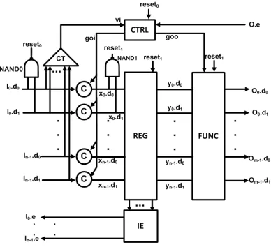
Global Reset Insertion
As mentioned, the Global Reset (GR) is connected to Initial Processes (IP). IP will output reset data once GR is asserted. There must be enough IP so that reset data can reach all processes in the system.
For a system with GRS, once GR is asserted, all channel wires between different processes are driven to 0s. When GR is deasserted, Non-Initial Processes (NIP) wait for valid data. Only IP such as initial buffers and sources start by sending valid data. Since QDI systems are working with GRS, the generated valid data from initial buffers and sources must be able to reach all processes in the system. Otherwise, part of the system stays idle and doesn’t function at all.
When the system is modified from GRS to WRS, the number of processes don’t change, neither do the connections among different processes. There-fore, reset data generated from initial buffers and sources must be able to reach all processes in the system with WRS. It is sufficient to have initial buffers and sources as IP.
Although reset data can always reach all processes in the system with WRS, reset time can vary depending on the choice of Local Reset Input (LRI). If reset data arrives at LRI of a process late, reset data will be gen-erated late at the output of the process which will affect the resetting of the next process. In the end reset time is large. Therefore, LRI should be chosen as the first input of a process that gets reset data during reset phase.
A systematic approach of finding LRI is demonstrated in this chapter. First, the system is modelled as a directed graph G≡ (V, E). V is a set of vertices while E is a set of edges. Each vertex v ∈ V represents a process while each edge as an ordered pair e ≡ (vi, vj) ∈ E represents a channel connecting processvi to process vj. If there is an edge (vi, vj)∈E, vertexvj is adjacent to vertex vi.
Each edge connects exactly two vertices. Fork is implemented inside vertices. For example, if one output Ou from process u needs to connect to inputs Iv and Iw of two different processes v and w, instead of connecting the same output Ou to both Iv and Iw, two identical copies of outputs Ou0
and Ou1 will be generated from u and respectively connect to Iv and Iw. In
addition, there is no edge starting from and ending with the same vertex. A path from vertex u to vertex v is a sequence of edges starting from u
in the QDI systems is connected but not necessarily strongly connected.
4.1
Breadth First Search (BFS)
As introduced in [4], Breadth First Search (BFS) systematically explores edges of G to discover every vertex that is reachable from the root vertex
v. It also generates a Breadth-First Tree (BFT) whose root is v. The tree contains all reachable vertices from v.
The pseudocode of BFS is shown in Figure 28. The algorithm has Gand
v as inputs. Each vertex in Ghas two attributes, color and parent. Color is used to distinguish different states of a vertex. Initially all vertices are white. When a vertex is traversed the first time, it becomes gray. If all adjacent vertices of a gray vertex have been traversed, it becomes black. When a vertex v is traversed the first time in the course of scanning the adjacent vertices of an already traversed vertex u, u is the parent of v and v is the child of u.
BF S(G, v) works as follows. Line 2 creates an empty queue Q which is used to store the first-time traversed vertices. Q.enqueue(v) inserts vertex
v into Q while Q.dequeue() removes the first element in Q and returns it. Line 3 creates an empty tree T. T.add(u, v) inserts v into T as the child of
u. After the execution of the algorithm,T is BFT. Line 4-6 mark all vertices white and set their parent NIL. The root vertex v is first marked gray and added into T and Q as in Line 7-9. The while loop in Line 10-18 iterates as long as Qis not empty. During each iteration, the first elementnis removed from Q. If any of its adjacent vertices s is white which indicates s hasn’t been traversed, s will be marked gray and s’s parent is set to n. s is then inserted into T and Q. When all its adjacent vertices have been traversed, n is marked black.
4.2
Breadth First Search with Multiple Roots
(BF-SMR)
1 p r o c e d u r e BFS(G, v)
2 c r e a t e an empty queue Q
3 c r e a t e an empty t r e e T
4 f o r e a c h v e r t e x u ∈ V(G) 5 u. c o l o r = w h i t e
6 u. p a r e n t = NIL 7 v. c o l o r = g r a y 8 T . add ( n u l l , v) 9 Q. enqueue (v)
10 w h i l e Q i s not empty 11 n = Q. dequeue ( )
12 f o r e a c h s ∈ n. a d j a c e n t v e r t i c e s 13 i f s. c o l o r = w h i t e
14 s. c o l o r = g r a y 15 s. p a r e n t = n 16 T . add (n, v)
17 Q. enqueue (s)
[image:48.612.94.356.131.391.2]18 n . c o l o r = b l a c k
Figure 28: Pseudocode of Breadth First Search (BFS)
4.2.1 Pseudocode
The pseudocode of BFSMR is shown in Figure 29. Only Line 7-10 are dif-ferent from Figure 28. Instead of inserting single root intoT andQ initially, all vertices that represent IP are inserted.
4.2.2 Proof of Correctness
The correctness of the pseudocode is proved with loop invariant: Qcontains nothing or all gray vertices.
4.2.2.1 Initialization Before the iteration of the while loop, Qcontains all gray vertices that represent IP in the system as shown in Line 7-10. Processes other than IP in the system are marked white in Line 4-6. The loop invariant is true.
1 p r o c e d u r e BFSMR(G, V )
2 c r e a t e an empty queue Q
3 c r e a t e an empty t r e e T
4 f o r e a c h v e r t e x u ∈ V(G) 5 u. c o l o r = w h i t e
6 u. p a r e n t = NIL
7 f o r e a c h v e r t e x t h a t r e p r e s e n t s IP 8 v. c o l o r = g r a y
9 T . add ( NIL , v) 10 Q. enqueue (v)
11 w h i l e Q i s not empty 12 n = Q. dequeue ( )
13 f o r e a c h s ∈ n. a d j a c e n t v e r t i c e s 14 i f s. c o l o r = w h i t e
15 s. c o l o r = g r a y 16 s. p a r e n t = n 17 T . add (n, v)
18 Q. enqueue (s)
[image:49.612.94.365.132.406.2]19 n . c o l o r = b l a c k
Figure 29: Pseudocode of BFS with Multiple Roots
contains all gray vertices, after this removal of n which is marked black, Q
contains nothing or all gray vertices.
Another operation related toQis the insertion inside the for loop in Line 13-18. For each adjacent vertex of n, if it is white, it is marked gray and inserted into Q. Since the vertex inserted into Q has always been marked gray beforehand, ifQcontains nothing or all gray vertices before the for loop,
Qcontains nothing or all gray vertices after the for loop. Therefore, the loop invariant is maintained.
4.2.2.3 Termination There are two for loops and one while loop in the pseudocode. The two for loops will terminate because the number of total vertices and IP are finite.
vertex is removed from Q and marked black. Therefore, after finite number of iterations, Q will become empty, all vertices will be marked black and
5
Iterative Multiplier
In this chapter, an 8-bit iterative multiplier is implemented to evaluate whether a QDI system can be reset properly with WRS and start normal operation without deadlock. The behavior of the iterative multiplier is de-scribed by CHP in the Appendix.
5.1
Iterative Multiplier
The iterative multiplier shown in Figure 30 stores two multiplicants I0 and
[image:51.612.245.363.348.549.2]I1 in register m0 and m1. m0 is a parallel-in serial-out register. It receives 8-bit data and outputs it bit by bit starting with the Least Significant Bit (LSB). m1 receives 8-bit data and outputs the same data for eight times. If the bit fromm0 is 1, the multiplexermuxaccepts data fromm1 and outputs it to the adder add8; otherwise it outputs 0 to add8.
Figure 30: Iterative Multiplier
Most of processes in the multiplier are implemented with PCHB tem-plates. The rest are special blocks: Demuxis an AP that starts by sending 0 to add8. A Source process continues sending 0 to one of the inputs ofmux. Some functions such as copy, merge and split are implemented by slack-zero processes.
5.2
Simulation
The multiplier is simulated with an environment that accepts data from O, applies some function to the received data and sends higher and lower bytes of the results to I0 and I1 respectively. Therefore the system is closed and operates forever.
The multiplier resets and operates correctly under different process tech-nologies, process corners and operating voltages. Reset time is shown in Figure 31. The X-axis specifies different simulation conditions. “LP” refers to TSMC 40nm Low-Power technology while “GS” refers to TSMC 40nm General-Purpose technology. The number following “LP” or “GS” is the op-erating voltage. For example, “06” is 0.6V while “10” is 1V. Three series of data represent three different process corners, i.e. TT (Typical NMOS, Typical PMOS), SF (Slow NMOS, Fast PMOS) and FS (Fast NMOS, Slow PMOS).
Figure 31: Reset Time for Different Process Corners
Figure 32: Cycle Time for Different Process Corners
Figure 33: Reset Time with Additional Global Reset
6
Conclusion
In this thesis, reset schemes for QDI systems have been examined. Circuit implementation and operation protocol for both GRS and WRS have been discussed. Reset time of systems with WRS is dependent on the choice of LRI. An algorithm has been proposed to systematically choose the LRI in order to shorten the reset time. The proposed WRS has been applied to an iterative multiplier that operates correctly under different operating conditions.
In some sense WRS is a more general reset scheme for QDI systems than GRS. LR in WRS can be changed to GR in order to shorten reset time. This has been illustrated by the multiplier application. Once all LR for WRS are changed to GR, WRS changes to GRS. Therefore, GRS is a special case of WRS. If there are more LR in the system, the large network of rails and buffers distributing GR can be removed. All reset signals become local. On the other hand, having more GR will reduce the reset time of the QDI system. The choice of the number of GR is application dependent.
Appendices
CHP Description of The Iterative Multiplier
process mult()(I0?, I1?: byte; O!: word) chp{
var x0, x1: byte; var y: word;
*[I0?x0, I1?x1; y:=x0 * x1; O!y] }
meta{
instance m0: mult0; instance m1: mult1; instance mx: mux; instance ad: add8; instance dx: demux; instance r1: rmsb; instance r0: rlsb; instance r: result;
connect I0, m0.I;
connect I1, m1.I;
connect m0.O, mx.C; connect m1.O, mx.I; connect ad.I0, mx.O; connect ad.I1,dx.O0; connect ad.O, dx.I;
connect ad.LSB, r0.I;
connect dx.O1, r1.I;
connect all j:0..7: r.I0[j], r0.O[j];
connect r.I1, r1.O;
connect O, r.O; }
process mult0()(I?: byte; O!: bit) chp{
var x: byte;
*[I?x; O!x[0]; O!x[1]; O!x[2]; O!x[3]; O!x[4]; O!x[5]; O!x[6]; O!x[7]] }
process mult1()(I?, O!: byte) chp{
var x: byte;
}
process mux()(I?, O!: byte; C?: bit) chp{
var c: bit; var x: byte; *[C?c, I?x; [ c -> O!x
[]~c -> O!0]] }
process demux()(I?, O0!, O1!: byte) chp{
var x: byte;
*[O0!0; <<;i:0..6:I?x; O0!x>>; I?x; O1!x, O0!0] }
process add8()(I0?, I1?: byte; O!: byte; LSB!:bit) chp{
var x0, x1, yp: byte; var y: word;
*[I0?x0, I1?x1; y:=x0+x1; <<,i:0..7: yp[i]:=y[i+1]>>; O!yp, LSB!y[0]] }
process rmsb()(I?, O!: byte) chp{
var x: byte; *[I?x; O!x] }
process rlsb()(I?: bit; O[0..7]!: bit) chp{
var y: byte;
*[ <<; i:0..7: I?y[i]>>; <<, i:0..7:O[i]!y[i]>> ] }
process result()(I0[0..7]?: bit; I1?: byte; O!: word) chp{
var y: word; var x0, x1: byte;
References
[1] A. J. Martin and M. Nystrom, “Asynchronous techniques for system-on-chip design” Proc. IEEE Volume 94, Issue 6, pp. 1089-1120, Oct. 2006.
[2] A. J. Martin, “The limitation to delay-insensitivity in asynchronous cir-cuits” Sixth MIT Conference on Advanced Research in VLSI, pp. 263-278, 1990.
[3] A. M. Lines “Pipelined Asynchronous Circuits” M.S. thesis, CS, Caltech, Pasadena, CA, 1995
[4] T. H. Cormen, C. E. Leiserson, R. L. Rivest and C. Stein, “Introduction to Algorithms”, 3rd ed. MIT Press and McGraw-Hill 2009, Ch. 22.4, pp. 449-451.