LCD-4 'SERIES
THIS MANUAL APPLIES TO UNITS BEARING SERIAL NUMBER PREFIXES
A-C
INSTRUCTION MANUAL
FOR
REGULATED POWER SUPPLIES
LCD-4 'SERIES
THIS MANUAL APPLIES TO UNITS BEARING SERIAL NUMBER PREFIXES
A-C
This manual provides instructions intended for the operation of Lambda power supplies, and is not to be reproduced without the written consent of Lambda Electronics. All information contained herein applies to all LCD-4 models unless otherwise specified.
L~~DA ELECTRONICS MELVILLE, L.I., N.Y.
MAIN PLANT TELEPHONE: 516 MYrtle 4-4200
TABLE OF CONTENTS
SECTION
SPECIFICATIONS AND FEATURES
THEORY OF OPERATION
OPERATING INSTRUCTIONS
Basic Mode of Operation
Connections for Operation
Supply-Load Connections
Operation After Protective Device Shutdown
MAINTENANCE
General
Trouble Analysis
Checking Transistors and Capacitors
Printed Circuit Board Maintenance Techniques
Trouble Chart
Performance Checks
Adjustment of Calibration Control R13
SERVICE
PARTS ORDERING
PAGE
1
4
5
5
5
6
8
8
8
8
9
9
10
11
12
13
SPECIFICATIONS AND FEATURES
Specifications apply for all models.
DC OUTPUT--Vo1tage regulated for line and load. See table I for voltage and
current ratings. Dual outputs are independent of one another. Both outputs are
floating.
TABLE I
VOLTAGE AND CURRENT
RANGES
VOLTAGE MAXIMUM CURRENT (AMPS) AT
MODEL RANGE AMBIENT TEMPERATURE
(EACH SIDE) 40°C 50°C 60°C 71 °c
LCD-4-11 0-7 1.8 1.5 1.2 0.7
0-7 1.8 1.5 1.2 0.7
LCD-4-12 0-18 1.0 0.8 0.65 0.4
0-7 1.8 1.5 1.2 0.7
LCD-4-13 0-32 0.6 0.53 0.4 0.24
0-7 1.8 1.5 1.2 0.7
LCD-4-22 0-18 1.0 0.8 0.65 0.4
0-18 1.0 0.8 0.65 0.4
LCD-4-23 0-32 0.6 0.53 0.4 0.24
0-18 1.0 0.8 0.65 0.4
LCD-4-33 0-32 0.6 0.53 0.4 0.24
0-32 0.6 0.53 0.4 0.24
LCD-4-44 0-60 0.33 0.3 0.24 0.15
0-60 0.33 0.3 0.24 0.15
LCD-4-55 0-120 0.12 0.12 0.12 0.075
0-120 0.12 0.12 0.12 0.075
LCD-4-152 15 ± 5% 1.5 1.3 1.0 0.6
(Fixed) 15 ± 5% 1.5 1.3 1.0 0.6
Current range must be chosen to suit the appropriate maximum
ambient temperature. Current ratings apply for entire
volt-age range.
REGULATED VOLTAGE OUTPUT
Regulation (line) • 0.01 percent plus 1.0 millivolt for input
varia-tions from 105-132 or 132-105 volts AC
Regulation (load) • • • • • • 0.01 percent plus 1.0 millivolt for load varia-tions from no load to full load or full load to no load
Remote Programming
External Resistor • Nominal 1000 ohms/volt output
Programming Voltage • • One-to-one voltage change
Ripple and Noise •• 250 microvolts rms; 1 millivolt peak to peak
with 57-63 Hz input
Temperature Coefficient • • • Output change in voltage (0.01%
+
0.3 mv)/oC usingan external programming resistor, less than (0.015%
+
0.3 mv)/oC with internal resistorRemote Sensing Provision is made for remote sensing to eliminate
effect of power output lead resistance on DC reg-ulation.
AC INPUT -- 105-132, 205-265 or 187-242 C'V" option) volts AC at 47-440Hz.
input power*:125 Watts. Ratings apply for 57-63Hz; at 47-57Hz
derate current 10% for each ambient temperature given in table
63-440Hz, consult factory for details of operation.
Maximum input
I. For
~~ith output loaded to full 40°C rating and input voltage 132 volts AC, 60 Hz
OVERLOAD PROTECTION
Thermal • • • •
Electrical External
Thermostat, resets automatically when over tem-perature condition is eliminated
Automatic electronic current limiting circuit, limits output current to a preset value less than llO% of 40°C current rating. Automatic limiting protects the load and power supply when external overloads and direct shorts occur.
Internal • • • • • • • • Fuse Fl provides protection against internal cir-cuit failure in conjunction with overvoltage pro-tector option.
INPUT AND OUTPUT CONNECTORS -- Tenninal blocks on rear of chassis.
OPERATING AMBIENT TEMPERATURE RANGE AND DUTY CYCLE--Continuous duty from -20°C to 71°C ambient with corresponding load current rat-ings for all modes of operation.
STORAGE TEMPERATURE -(non-operating)
CONTROLS
PHYSICAL DATA
Size ...•..•... 4-29/32" X 4-29/32" x 5-1/4"
Weight ... 7 1bs. net; 8 1bs. shipping Finish ... Grey, FED STD 595 No. 26081
MOUNTING - Three surfaces, each with tapped mounting holes, can be utilized for
mounting this unit. All LCD-4 power supplies can be mounted with, Top,
Front, or Rear facing up. Top, Front, or Rear must be in a horizontal
plane. Refer to figure 13 for mounting details.
MODEL OPTIONS
"V" OPTION ... Standard LCD-4 power supplies can be obtained for 205-265 VAC, 47-440 Hz input or 187-242 VAC, 47-440 Hz input.
See nameplate for AC input rating. See
schematic diagram for rewiring of AC input.
"s"
OPTION ... Standard LCD-4 power supplies are avail-able for use with Lambda Systems Power Sequencer or Systems Power Protector.ACCESSORIES
On models LCD-4-l52 specified with the
"s"
option, resistors R2l and R12l are replaced by a jumper.Rack Adapter ... Rack adapters LRA-10, LRA-ll, and LRA-13 with or without chassis slides are avail-able.
Overvo1tage Protector ... Externa11y mounted, Overvo1tage Protectors LH-OV-4, LH-OV-5, and LH-OV-6 are avail-able for use with Lambda LCD-4-11 through
LCD-4-44 power supplies. On model
LCD-4-152 use overv.ol·tage pro.tector L-20"0V-15.
Control Panel ... A11 LCD-4 power supplies may be obtained with a Systems Power Control Panel, SP-5. This unit, mounted on rack adapters LRA-IO or LRA-11 and used with a Systems Cable
Metering
IM-LCD-4
or Auxiliary Cable, provides an on-off switch, voltage control and pilot light. A single panel controls both master (M) and slave (S) units of the power supply.
Panel. ... A Systems Metering Panel, SMP-5 may be used in conjunction with the LCD-4 power supplies. The panel, mounted in rack adapter LRA-IO or LRA-11 and used with a Systems Cable, contains a voltmeter and an ammeter, each with three ranges and pushbutton selector
switch. The selector switch allows
moni-toring of the voltage and current of any of up to 16 outputs.
THEORY OF OPERATION
GENERAL
The text in this section refers to circuit designations for the "M" unit of the LCD-4 power supply, however the discussion is equally applicable to the "S" unit which has electrically identical components in the 100 series except for CRl12, which
is used in the "S" unit only.
The Lambda Power supply consists of an AC input circuit and transformer; a bias supply consisting of an auxiliary rectifier and filter, and preregu1ator*; a main regulator circuit consisting of the main rectifier and filter, a series regulator, emitter follower driver, a current comparator'i:, a voltage comparator;':, an amp1ifi er'i:, current and voltage sensing networks and a voltage reference circuit*.
7~his circuit element is part of integrated circuit (IC1) in the supply.
The circuit arrangement is shown in b+ock diagram form, figure 11. The
circuit-ry is discussed with reference to the block diagram and the schematic diagram.
FUNCTIONAL DESCRIPTION
Single phase input power is applied to transformer T1 through the which contains a thermostat to protect the supply against overheating. Tl supplies secondary power for both "M" and "S" units.
input circuit Transformer
The main rectifier, a full wave rectifier, provides the power which is filter-ed by capacitor C6 and then regulatfilter-ed via a series regulator and deliverfilter-ed to the
output. Half-wave auxiliary rectifier CR1 provides voltage filtered by capacitor
C1 for the preregu1ator located in IC1. The reference element, powered by the
pre-regulator, provides a reference voltage for the current comparator and the voltage comparator.
Constant voltage circuit operation is determined by changes in the load which cause a change in one input to the voltage comparator. A second input to the com-parator is a reference voltage that is developed by a constant current of 1
milli-ampere flowing in divider element R8. The comparator compares the output voltage
change with the reference voltage resulting in an error signal at the output of the comparator.
The error signal from the comparator is then current amplified by drivers Q1
and Q2. The amplified signal from the drivers controls the voltage across the
ser-ies regulator Q3, which functions as the active regulating element in the supply.
* Current limit circuit operation is determined by changes in the load. The
current comparator samples load current through current sensing resistor R7. When
the voltage drop across R7 increases to the preset voltage reference determined by
R6, R9, and Rl3, the current comparator conducts. Thus, when the output current
rat-ing of the unit is exceeded, the current comparator conducts, decreasrat-ing the current through driver Ql, resulting in an increase of voltage across the series regulator and a decrease of the output voltage, effectively limiting the output current to a
safe value. The current limit value is determined by fixed resistors R6, R7, R9 and
When operating conditions approach short circuit, the output voltage decreases. Since the voltage determined by R13 is proportional to the output voltage, when the output voltage decreases, the amplifier is biased into turn on at lower and lower load currents until output voltage decreases to zero and current decreases to a pre-determined low value.
*
The following theory applies to model LCD-4-l52.Current limit circuit operation is determined by changes in the load. When
load current increases above the rated current value, the voltage drop across
cur-rent limit potentiometer R13 increases causing the amplifier to turn on. With the
amplifier conducting the current to driver Ql decreases, limiting the base current to series regulator Q3, which results in an increase of voltage across the series regulator and a decrease of the output voltage, effectively limiting the output
cur-rent to a safe value. The current limit value is determined by the factory setting
of current limit potentiometer R13.
When operating conditions reach short circuit, the output voltage value de-creases to zero and the current dede-creases to a predetermined current limit value and remains unchanged.
OPER~ING INSTRUCTIONS BASIC MODE OF OPERATION
This power supply operates as a constant voltage source provided the load
cur-rent does not exceed the rated value at 40°C. For continuous operation, load
cur-rent must not exceed the rating for each ambient temperature and will remain limited to less than 110% of 40°C rating.
CONNECTIONS FOR OPERATION
NOTE: Make all connections to the unit before applying AC
input power.
Ground Connections. The Lambda power supply can be operated either with negative
or positive output terminal grounded. Both positive and negative ground connections
are shown in the diagrams for all suggested output connections illustrated in this manual.
Connection Terminals. Make all connections to the supply at the terminal blocks on
the rear of the supply. Apply input power to terminals 1 and 2; always connect the
ungrounded (hot) lead to terminal 1.
The supply positive terminal is brought out to terminals 6 (M unit) and 14
(S unit). The supply negative terminal is brought out to terminals 4 (M unit) and
12 (S unit). Recommended wiring of the power supply to the load and selection of
wiring is shown in figures 1 through 10. Selection of proper wiring is made on the
basis of load requirements. Make all performance checks and measurements of current
or voltage at the rear output terminals. Connect measuring devices directly to
ter-minals or use the shortest leads possible.
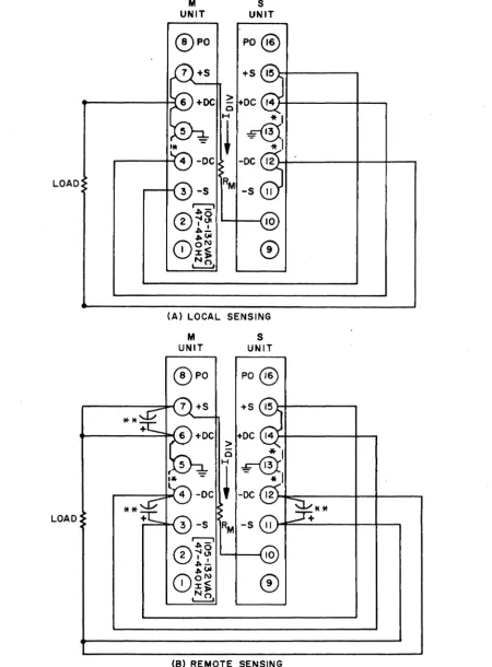
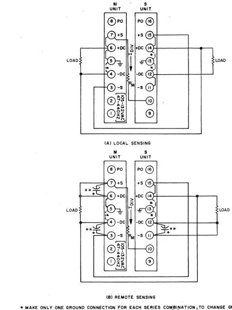
SUPPLY LOAD CONNECTIONS
Connections For Operation as a Constant Voltage Source
The load regulation of the power supply at the load may change when using the supply as a constant voltage source and connecting leads of practical length are
used. To minimize the effect of the output leads on load regulation, remote
sens-ing is used. Recommended types of supply-load connections with local or remote
sen-sing are described in the following paragraphs.
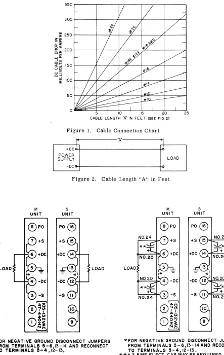
Refer to figure 1 to determine voltage drop for particular cable length, wire
size and current conditions. Lead lengths must be measured from supply terminals to
load terminals as shown in figure 2.
Two-Wire Connection, Figure 3. The two-wire connection, with local sensing, is the
connection suitable for applications with relatively constant load.
Four-Wire Connection, Figure 4. The four-wire connection with remote sensing,
pro-vides complete compensation for the DC voltage drops in the connecting cables.
Sensing leads should be a twisted pair to minimize AC pick-up. A 2.5mf, elect,
capacitor may be required between output terminals and sense terminals to reduce noise pick-up.
Programmed Voltage Connections, Using External Resistor, Figu're 5. Discrete voltage
steps can be programmed with a resistance voltage divider valued at 1000 ohms/volt
and a shorting-type switch as shown in figure 5. When continuous voltage variations
are required, use a variable resistor with the same 1000 ohms/volt ratio in place of
the resistive voltage divider and shorting-type switch. Use a low temperature
co-efficient resistor to assure most stable operation. Before programming, adJust
programming resistor for zero resistance and set voltage adjust controls to the min-imum rated output voltage.
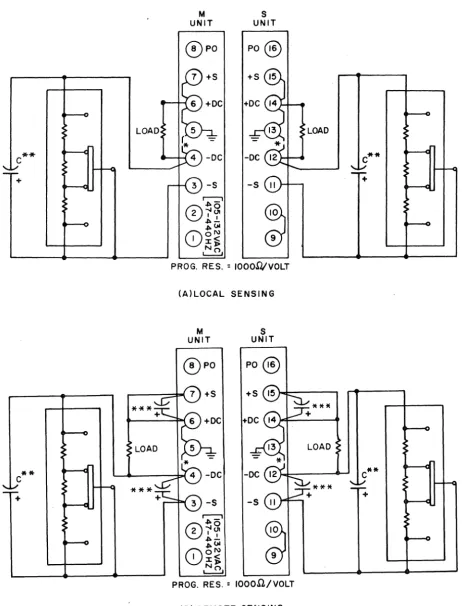
As shown in figure 5, voltages can be programmed utilizing either local or re-mote sensing connections, as desired.
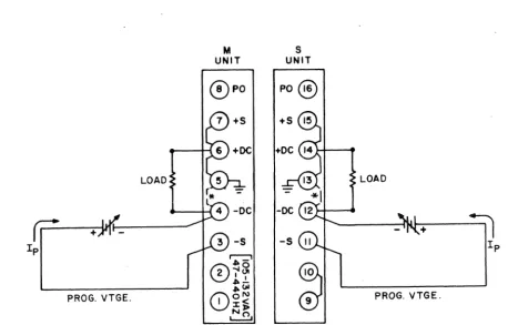
Programmed Voltage Connections Using Programming Voltage, Figure 6. The power
sup-ply voltage output can be programmed with an externally connected programming power
supply. The output voltage of the programmed supply will maintain a one-to-one
ratio with the voltage of the programming supply.
The programming supply must have a reverse current capability of 1.5 rna. min-imum.
Alternatively, when supplies with less than 1.5 rna reverse current capability are used, a resistor capable of drawing 1.5 rna. at the minimum programming voltage
must be connected across the output terminals of the supply. This programming
sup-ply must be rated to handle all excess resistor current at the maximum programming voltage.
ation. A maximum of 250 volts can be connected between either the +DC or -DC ter-minal and chassis ground with a maximum voltage capability of 240 volts possible for
model LCD-4-55. 7~If a cOllmon load is used, the maximum current rating of the unit
with the lower current rating must not be exceeded.
7d~ A common load can not be used with model LCD-4-l52.
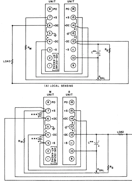
Figure 7 (or, as applicable, 7A) shows connections for either loca~ or remote
sensing in a series connection where the voltage control of each unit functions in-dependently to control the output, and where the S unit does not track the M unit.
Units M and S are shown connected for auto-series operation in figure 8 and 9. Figure 8 (or, as applicable, 8A) shows the series connection diagram which would be
suitable for use in most applications where tracking is desired. Using externally
connected meters, first set the S unit output voltage adjust control for zero
out-put, then set M unit output voltage adjust control for desired output voltage.
Re-adjust S unit output voltage to agree with the output voltage of the M unit. The S
unit will track any change in M unit output voltage made with the M unit voltage adjust control.
Voltage divider RM must be used during auto-series operation. Variations of RM according to the desired output voltage of the supply* may be found by applying the following formula:
= Eout
I div
h E .
were out 1.S
Idiv may vary pectively.
the desired supply output voltage and I div is the divider current. between a minimum and maximum value of one and two milliamperes
res-* On hybrid power supplies (LCD-4-l2, -13, -23) desired master output voltage must never exceed the slave maximum output voltage rating.
Figure 9 (or, as applicable, 9A) shows the series connection diagram suitable for applications where more precise voltage tracking due to temperature changes is required.
Resistor RBAL should be one-watt, 1 - 2 kilohm resistor. This value would per-mit wide-range compensation for manufacturing differences inherent in the components used in each unit. Resistors RS and RM function in the voltage sensing circuits of both units, enabling the S unit to reference its output voltage to that of the M unit. Select RM and RS on the basis of 500 ohm to 1000 ohm per volt of M unit output
volt-age. RM must equal RS.
Capacitor C, used to eliminate stray AC pickup, is rated at 2.5 mf, 200V for
models LCD-4-ll thru LCD-4-44 and LCD-4-l52. On model LCD-4-55, C is rated at 1.4
mf 400V.
Connections For Parallel Operation
The current capability of LCD-4 power supplies can be extended by parallel
op-eration of LCD-4 power supplies of equa17~ voltage capacities. Units "M" and
"s"
are shown connected for parallel operation in figure 10. One power supply
desig-nated the "master" or M unit controls its own output as well as the output of the second power supply, designated the "slave" or S unit.
Unit S operates to regulate its current in a ratio to' that of the M unit by comparing the current in its internal sampling resistor with that current sampled by the master internal sampling resistor.
OPERATION AFTER PROTECTIVE DEVICE SHUTDOWN
Thermostat Shutdown
The thermostat opens the input circuit only when the temperature of the internal
heat sink exceeds a maximum safe value. The thermostat will automatically reset when
the temperature of the heat sink decreases to a safe operating value. After
elimin-ating the cause(s) for overheelimin-ating and allowing time for the power supply to cool to a proper temperature, resume operation of the supply.
Fuse Shutdown
Fuse will blow when the maximum rated current value for the fuse is exceeded. Fatigue failure of fuses can occur when mechanical vibrations from the installation. combine with thermally induced stresses to weaken the fuse metal. Many fuse fail-ures are caused by a temporary condition and replacing the blown fuse will make the fuse protected circuit operative. When the LCD-4 supply is used with the overvolt-age protector option, fuse Fl will provide load protection against internal compon-ent failure.
. MAINTENANCE
GENERAL
This section describes trouble analysis routine, replacement procedures, cali-bration and test procedures that are useful for servicing the Lambda LCD-4 power
supply. A trouble chart is provided as an aid for the troubleshooter. The text of
the trouble chart refers to component designations of unit M of the LCD-4 supply, but it is equally applicable for unit S which has identical components designated
in the 100 series. Refer to the section on specifications and features for the
min-imum performance standards.
TROUBLE ANALYSIS
Whenever trouble occurs, systematically check all fuses, primary power lines, external circuit elements, and external wiring for malfunction before trouble
shoot-ing the equipment. Failures and malfunctions often can be traced to simple causes
such as improper jumper and supply-load connections or fuse failure due to metal fatigue.
Use the electrical schematic diagram and block diagram, figure 11, as an aid
to locating trouble causes. The schematic diagram contains various circuit voltages
that are averages for normal operation. Measure these voltages using the conditions
for measurement specified on the schematic diagram. Use measuring probes carefully
CHECKING TRANSISTORS AND CAPACITORS
Check transistors with an instrument that has a highly limited current
capabil-ity. Observe proper polarity to avoid error in measurement. The forward transistor
resistance is low but never zero; backward resistance is always higher than the for-ward resistance.
For good transistors, the forward resistance for any junction is always great-er than zgreat-ero.
Do not assume trouble is eliminated when only one part is replaced. This is
especially true when one transistor fails, causing other transistors to fail.
Re-placing only one transistor and turning power on, before checking for additional defective components could damage the replaced component.
When soldering semi-conductor devices, wherever possible, hold the lead being soldered with a pair of pliers placed between the component and the solder joint to provide an effective heat sink.
NOTE: The leakage resistance obtained from a simple resistance check of
a capacitor is not always an indication of a faulty capacitor. In all
cases the capacitors are shunted with resistances, some of which have low
values. Only a dead short is a true indication of a shorted capacitor.
PRINTED CIRCUIT BOARD MAINTENANCE TECHNIQUES
1. If foil is intact but not covered with solder it is a good contact. Do
not attempt to cover with solder.
2. Voltage measurements can be made from either side of the board. Use a
needlepoint probe to penetrate to the wiring whenever a protective coating is used
on the wiring. A brass probe can be soldered to an alligator clip adapted to the
measuring instrument.
3. Wherever possible use a heat sink when soldering transistors.
4. Broken or damaged printed wiring is usually the result of an imperfection,
strain or careless soldering. To repair small breaks, tin a short piece of hook-up
wire to bridge the break, and holding the wire in place, flow solder along the length of wire so that it becomes part of the circuitry.
5. When unsoldering components from the board never pryor force loose the
part; unsolder the component by using the wicking process described below:
(a) Select a 3/16 inch tinned copper braid for use as a wick; if braid
is not available, select AWG No. 14 or No. 16 stranded wire with 1/2 inch insulation
removed.
(b) Dip the wick in liquid rosin flux.
(c) Place the wick onto the soldered connection and apply soldering
iron onto the wick.
(d) When sufficient amount of solder flows onto the wick, freeing the component, simultaneously remove iron and wick.
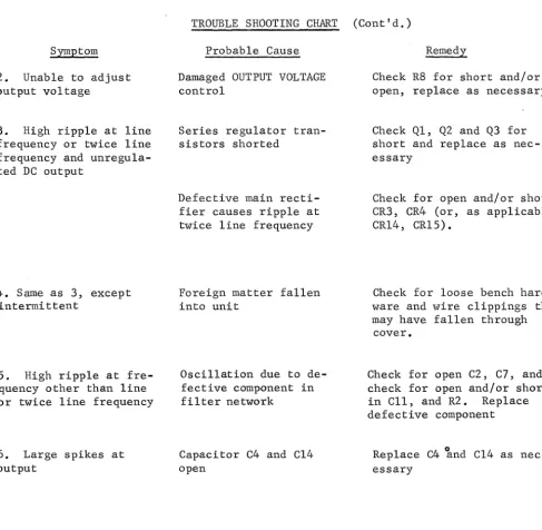
TROUBLE CHART
The trouble chart is intended as a guide for locating trouble causes, and is used along with the schematic diagram. When troubleshooting the S unit, add 100 to the component designations in the trouble chart.
The operating conditions assumed for the trouble chart are as follows:
(a) AC power of proper voltage and frequency is preset at input terminals.
(b) Either positive or negative terminal is connected to chassis ground.
(c) The power supply is connected for constant voltage with local sensing. See schematic; dotted lines indicate jumpers connected for local sensing operation.
Symptom
1. Zero volts DC output
TROUBLE SHOOTING CHART
Probable Cause
OUTPUT VOLTAGE Control turned fully CCW
Short circuit across
out-put of supply
Fl open
Series regulator sec-tion open
Shorted CR6 (or, as appli-cable, CR7)
Open CR8, CR9 or Rl
Current sensing resis~
tor open
Aux. rectifier CRI open
On S unit, jumper between 9 and 10 open
Remedy
Check OUTPUT VOLTAGE Con-trol for proper setting and correct as necessary
Check load and load con-nections, correct as nec-essary
Replace Fl; if it blows immediately, check for shorted diode CR7 transis-tors Ql, Q2, Q3 and capac-itors C7, C15, replace as necessary
Check Ql, Q2 and Q3 for open, replace as necessary
Check CR6 (or CR7) for short, replace as necessary
Check CR8, CR9 and Rl for open replace as necessary
Check R7 for open, R6 for short; R9 for open; re-place as necessary
Check CRl for open; re-place as necessary
Check S unit jumper
connec-tion to terminals 9
&
10Symptom
2. Unable to adjust
output voltage
3. High ripple at line frequency or twice line frequency and unregula-ted DC output
4. Same as 3, except intermittent
5. High ripple at
fre-quency other than line or twice line frequency
6. Large spikes at
output
PERFORMANCE CHECKS
TROUBLE SHOOTING CHART (Cont'd.)
Probable Cause
Damaged OUTPUT VOLTAGE control
Series regulator tran-sistors shorted
Defective main recti-fier causes ripple at twice line frequency
Foreign matter fallen into unit
Oscillation due to de-fective component in filter network
Capacitor C4 and C14 open
Remedy
Check R8 for short and/or open, replace as necessary
Check Ql, Q2 and Q3 for short and replace as nec-essary
Check for open and/or short CR3, CR4 (or, as applicable, CR14, CR15).
Check for loose bench hard-ware and wire clippings that may have fallen through
cover.
Check for open C2, C7, and check for open and/or short
in Cll, and R2. Replace
defective component
Replace c4 ~nd C14 as
nec-essary
Check the ripple and regulation of the power supply using the test connection
diagram shown in figure 12. Use suggested test equipment or equivalent to obtain
accurate results. Refer to SPECIFICATIONS AND FEATURES for minimum performance standards.
Set the differential meter, DC VTVM (John Fluke Model 80lH or equivalent) to
the selected power supply operating voltage. Check the power supply load regulation
accuracy while switching from the load to no-load condition. Long load leads should be a twisted pair to minimize AC pick-up.
Use a Variac to vary the line voltage from 105-132 or 132-105 volts AC and check the power-supply line regulation accuracy on the VTVM differential meter.
Use a VTVM, Ballantine 320 or equivalent, to measure rms ripple voltage of the power supply DC output. Use oscilloscope to measure peak-to-peak ripple voltage of the power supply DC output.
[image:14.620.80.567.47.523.2]ADJUSTMENT OF CALIBRATION CONTROL R13
Whenever Q3, R6, R7, R9, R13, R2l or ICI are replaced, and voltage and current
indications do not reflect maximum ratings, adjust R13 as follows. The adjustment
procedure requires that the power supply is removed from associated equipment, is at an ambient temperature of 25-30°C, and is stabilized and not operating.
1. Remove AC input power to the supply.
2. Break seal on wiper of R13 from resistor housing and turn to full OW
position.
3. Operate power supply for constant voltage with local sensing, connected
as shown in figure 3, with no external load.
4.* Turn voltage adjust control until rated output voltage is obtained.
5.* Apply load so that output current is 110% of 40°C rating for the unit.
6."/' Using an oscilloscope, Tektronix 503 or equivalent, observe unit output
voltage while adjusting R13 in a COW direction. Adjust R13 until output ripple increases sharply and oscilloscope pattern changes.
7.* Place a DC ammeter of appropriate scale across output terminals 4 and 6
of the supply. The meter indication shall be a maximum of 115% of 40°C rating for
the unit.
8.*' After adjustment is completed, remove AC input power to the supply and use glyptol sealant to seal wiper of R13 to resistor housing.
9."/' After sealing, check setting and repeat adjustment procedure if required.
* Perform alternate steps 4A through 8A for adjustment of R13 on model
LCD-4-l52.
4A. Turn voltage adjust control until an output voltage of 14.25 vdc is obtained.
SA. Apply load so that output current is 2.0 amperes.
6A. Using an oscilloscope, Tektronix 503 or equivalent, observe output
volt-age while adjusting R13 in a COW direction. Adjust R13 until output ripple increases sharply and oscilloscope pattern changes.
7A. After adjustment is completed, remove AC power input to the supply and
use glyptol sealant to seal wiper of R13 to resistor hopsing.
SERVICE
When additional instructions are required or repair service is desired, con-tact the nearest Lambda office where trained personnel and complete facilities are ready to assist you.
Please include the power supply model and serial number together with complete
details of the problem. On receipt of this infonnation, Lambda will supply service
data or advise shipping for factory repair service.
All repairs not covered by the warranty will be billed at cost and an estimate forwarded for approval before work is started.
PARTS ORDERING
Standard components and special components used in the Lambda power supply can
be obtained from the factory. In case of emergency, critical spare parts are
avail-able through any Lambda office.
The following information must be included When ordering parts:
1. Model number and serial number of power supply and purchase date.
2. Lambda part number.
3. Description of part together with circuit designation.
4. If part is not an electronic part, or is not listed, provide a
descrip-tion, funcdescrip-tion, and location of the part.
PARTS LIST
The electrical parts located on Lambda models LCD-4-U- LCD-4-55, and
LCD-4-152 are listed here. Parts for units M and S are listed separately by unit.
Parts common to a group of models are listed first. Unique parts of individual
models within the group are listed separately, by model, immediately following the
group common-parts listing. In addition there are separate listings of parts for
the V option and SP-5, SMP-5, and LHOV accessories.
COMMON PARTS UNIQUE PARTS
MODELS LCD-4-ll- LCD-4-55 MODEL LCD-4-ll UNIT M
& LCD-4-152
CIRC. LAMBDA CIRC. LAMBDA
DESIG. DESCRIPTION NO. DESIG. DESCRIPTION NO.
C1 Cap., elect., 40 mf CBP-40-036 C3 Cap., mylar, 0.001 mf CGK-10-004
-10 + 75%, 33 vdc ±10%, 200 vdc
C2 Cap., mylar, 0.047 mf CGL-47-018 C4 Cap., mylar, 0.1 mf CAM-10-012
±10%, .200 vdc ±10%, 200 vdc
C5, Not assigned C6 Cap., elect., 3,600 mf CBS-36-044
C8 -10 +100%, 20vdc
Cap., mylar, 1 mf CGN-1O-005 C7 Cap. , elect. , 450 mf CBR-45-075
±lO%, 200 vdc -10 + 100%, 25 vdc
Cap., mylar, 0.033 mf CGL-33-009 Cll Cap., mylar, 0.0033 mf CGK-33-003
C10 ±10%, 200 vdc
±10%, 400 vdc
C14, Same as C4 C12, Not assigned
C15
C13 CR3, Not assigned
C16 Cap., paper, 0.1 mf CAM-10-012
±10%, 200 vdc CR4, CR6
CR1 Rectifier FBL-00-030
CR7 Rectifier FBL-00-047 CR2, Not assigned
CR8, Rectifier FBL-00-030 CR5
CR9 CR10, Same as CR1
CR14, Same as CR7 CRll
CR12 Not assigned CR15, CR16
CR13 Same as CR1 CR17 Not assigned
CR22* Rectifier, zener diode FBM-Z139 thru
Q4 Not assigned CR2L
R1 Res., film, 8,660 ohms DCS-87-071 F1 Fuse, 5.0A, 8AG, FFR-05-000
±1%, 1/4 w "NORM-BLO"
R9 Res. , film, 10,000 ohms DCT-10-047 IC1 Integrated circuit FBT-00-031
±1%, 1/4 w Q1, Transistor, NPN FBN-L113
R10 Res. , comp., 36 megohms DCB-3665 Q2
±5%, 1/4 w Q3 Transistor, NPN FBN-36485
Rll Not assigned R2 Res. , comp., 220 ohms DCB-22ll R12 Res., comp., 68,000 ohms DCB-6831 ±10%, 1/4 w
±10%, 1/4 w R3 Res., comp., 2,200 ohms DEB-2221
R14, Not assigned ±10%, 1/2 w
R15 R4 Res., comp., 1,000 ohms DGB-1021
R16 Res., comp., 470 ohms DCB-4711 ±10%, 1 w
±10%, 1/4 w R5 Res., comp., 1,200 ohms DCB-1221
R22 Not assigned ±10%. 1/4 w
R23 Res., comp., ±10%,1/4w
100 , 000 ohms DCB-1041 XF1 Fuseholder HRM-00-016
UNIQUE PARTS (Cont) UNIQUE PARTS (Cont) MODEL LCD-4-11 UNIT M (Cont) MODEL LCD-4-13 UNIT M
CIRC. LAMBDA CIRC. . LAMBDA
DESIG. DESCRlPTION NO. DESIG. DESCRlPTION NO.
R6 Res. , film, 249 ohms DCR-25-034 C3 Cap., mylar, 0.001 mf CGK-10-004
±1%, 1/4 w ±10%, 200 vdc
R7 Res., WW, 0.25 ohms DFM-25-016 C4 Cap., mylar, 0.1 mf CAM-10-012
±5%, 5 w ±10%, 200 vdc
RB Res., var., ww or cermet, DNT-lO-045 C6 Cap. , elect., 1,100 mf CBS-ll-042 10,000 ohms ±10%, 3/4 w -10 + 100%, 60 vdc
R13 Res., var., ww, 100 ohms DNR-10-046 ±20%, 2 w
C7 Cap., elect., 175 mf
-10 + 100%, 50 vdc
CBR-17-073 R17 Not assigned Cl1 Cap., mylar, 0.0022 mf CGK-22-00B
thru ±10%, 200 vdc
R21 C14, Same as C4
Sl Thermostat FKA-155-020 C15
T1 Transformer ABA-CD4-11 CR3, Not assigned MODEL LCD-4-12 UNITM CR4, CR6
C3 Cap., mylar, 0.001 mf CGK-10-004 CR7 Rectifier FBL-00-065
±10%, 200 vdc CRB, Rectifier FBL-00-030
C4 Cap., mylar, 0.1 mf CAM-10-012 CR9
±10%, 200 vdc CR14 Same as CR7
C6 Cap., elect., 2,100 mf CBS-21-043 thru
-10 + 100%, 35 vdc CR16
C7 Cap., elect., 2BO mf CBR-2B-074 CR17 Not assigned -10 + 100%, 40 vdc CR1B, Same as CRB Cl1 Cap., mylar, 0.0033 mf CGK-33-003 CR19
±10%, 200 vdc CR20, Not assigned
C14, Same as C4 CR2l
C15 F1 Fuse, 1.5A, BAG, FFR-01-500
CR3, Not assigned "NORM-BLO"
CR4, IC1 Integrated circuit FBT-00-031
CR6 Q1, Transistor, NPN FBN-L109
CR7 Rectifier FBL-00-047 Q2
CRB, Rectifier FBL-00-030 Q3 Transistor, NPN FBN-36220
CR9 Q5 Same as Q1
CR14 Same as CR7 R2 Res., comp., 470 ohms DCB-4711
thru ±10%, 1/4 w
CR17 R3 Res. , comp. , 22,000 ohms DEB-2231
CRl8 ,N ot assigned ±10%, 1/2 w
thru R4 Not assigned
CR2l R5 Res., comp., 1,200 ohms DCB-1221
F1 Fuse, 3.0A, BAG, FFR-03-000 ±10%,1/4w
"NORM-BLO" R6 Res. , film, 249 ohms DCR-25-034 IC1 Integrated circuit FBT-00-031 ±1%, 1/4 w
Q1, Transistor, NPN FBN-L1l3 R7 Res., ww, 1.0 ohm DFN-10-014
Q2 ±3%, 5 w
Q3 Transistor, NPN FBN-36485 R8 Res. , var. , cermet, DRT-40-009 R2 Res., comp., 220 ohms DCB-2211 40,000 ohms ±10%, 0.75 w
±10%, 1/4 w R13 Res., var., WW, 100 ohms DNR-10-046
R3 Res. , comp., 6, BOO ohms DEB-6821 ±20%, 2 W
±10%, 1/2 W R17 Same as R3
R4 Res. , comp., 1, BOO ohms DGB-1821 R18 Res. , comp., 820 ohms DCB-8211
±10%, 1 W ±10%, 1/4 W
R5 Res. , compo , 1,200 ohms DCB~1221 R19 Same as R2
±10%, 1/4 W R20, Not assigned
R6 Res. , film, 249 ohms DCR-25-034 R21
±1%, 1/4 W Sl Thermostat FKA-155-020
R7 Res., WW, 0.5 ohms ±5%, 5 W
DFM-50-015 T1 Transformer ABA-CD4-13
R8 Res., var., ww or cermet, DNT-23-072 MODEL LCD-4-22 UNITM 23,000 ohms ±10%, 3/4 w
C3 Cap., mylar, 0.001 mf CGK-10-004 R13 Res., var., ww, 100 ohms DNR-10-046
±10%, 200 vdc ±20%, 2 w
C4 Cap., mylar, 0.1 mf CAM-10-012 R17 Not assigned
±10%, 200 vdc thru
R21 C6 Cap." elect., 2,100 mf CBS-21-043
Sl Thermostat FKA-155-020 -10 + 100%, 35 vdc T1 Transformer ABA-CD4-12
UNIQUE PARTS (Cont) UNIQUE PARTS (Cont) MODEL LCD-4-22 UNIT M (Cont) MODEL LCD-4-23 UNIT M (Cont)
CIRC. LAMBDA CIRC. LAMBDA
~. DESCRIPTION NO. DESIG. DESCRIPTION NO.
C7 Cap., elect., 2BO mf CBR-2B-074 Fl Fuse 1.5A, BAG, FFR-01-500
-10 + 100%, 40 vdc "NORM-BLO"
ell Cap., mylar., 0.0033 mf CGK-33-003 ICI Integrated circuit FBT-00-031
±10%, 200 vdc Ql, Transistor, NPN FBN-L109
C14, Same as C4 Q2
C15 Q3 Transistor, NPN FBN-36220
CR3, Not assigned Q5 Same as Ql
CR4, R2 Res., comp., 470 ohms DCB-4711
CR6 ±10%, 1/4 w
CR7 Rectifier FBL-00-04'7 RS Res., comp., 22,000 ohms DEB-2231
CRB, Rectifier FBL-00-030 ±10%, 1/2 w
CR9 R4 Not assigned
CR14 Same as CR7 R5 Res., comp., 1,200 ohms DCB-1221
thru ±10%, 1/4 w
CR17 R6 Res. , film, 249 ohms DCR-25-034
CRIB Not assigned ±1%, 1/4 w
thru R7 Res., ww, 1.0 ohm DFN-I0-014
CR21. ±3%, 5 w
1<'1 Fuse, 3.0A, BAG, FFR-03-000 RB Res., var., cermet, DRT-40-009
'NORM-BLO" 40,000 ohms ±10%, 0.75 w
IC1 Integrated circuit FBT-00-031 R13 Res., var., ww, ' DNR-10-046 Ql, Transistor, NPN FBN-L1l3 100 ohms ± 20%, 2 w
Q2 R17 Same as RS
Q3 Transistor, NPN FBN-364B5 RIB Res., comp., B20 ohms DCB-B2ll
R2 Res., comp., 220 ohms DCB-22ll ±10%, 1/4 w
±10%, 1/4 w R19 Same as R2
RS Res., comp., 6,BOO ohms DEB-6B21 R20, Not assigned
±10%, 1/2 w R21
R4 Res., comp., 1 ,BOO ohms DGB-1B21 Sl Thermostat FKA-155-020
±10%, 1 w T1 Transformer ABA-CD4-23
R5 Res., comp., 1,200 ohms DCB-1221
±10%, 1/4 w MODEL LCD-4-33 UNIT M
R6 Res., film, 249 ohms DCR-25-034
CGK-10-004
±1%, 1/4 w C3 Cap., mylar, 0.001 mf
R7 Res., ww, 0.5 ohm DFM-50-015 ±10%, 200 vdc
±5%, 5 w C4 Cap., mylar, 0.1 mf CAM-10-012
RB Res., var., ww or cermet, DNT-23-072 ±10%, 200 vdc
23,000 ohms ±10%, 3/4 w C6 Cap., elect., 1,100 mf CBS-ll-042 R13 Res., var., ww, 100 ohms DNR-10-046 -10 + 100%, 60 vdc
±20%, 2 w C7 Cap., elect., 175 mf CBR-17-073
R17 Not assigned -10 + 100%, 50 vdc
thru Cll Cap., mylar, 0.0022 mf CGK-22-00B
R21 ±10%, 200 vdc
Sl Thermostat FKA-155-020 C14, Same as C4
T1 Transformer ABA-CD4-22 C15
CR3, Not assigned MODEL LCD-4-23 UNITM CR4,
Cap., mylar, 0.001 mf CGK-10-004 CR6
C3 CR7 Rectifier FBL-00-065
±10%, 200 vdc . CRB, Rectifier FBL-00-030
C4 Cap., mylar, 0.1 mf CAM-10-012 CR9
±10%, 200 vdc CR14 Same as CR7
C6 Cap., elect., 1,100 mf CBS-ll-042 thru
-10 + 100%, 60 vdc CR16
C7 Cap., elect., 175 mf CBR-17-073 CRIB, Same as CRB
-10 + 100%, 50 vdc CR19
Cll Cap., mylar, 0.0022 mf CGK-22-00B CR20, Not assigned
±10%, 200 vdc CR21
C14, Same as C4 F1 Fuse 1. 5A, BAG, FFR-01-500
C15 "NORM-BLO"
CRS, Not assigned IC1 Integrated circuit FBT-00-031
CR4, Q1, Transistor, NPN FBN-L109
CR6 Q2
CR7 Rectifier ·FBL-00-065 Q3 Transistor, NPN FBN-36220
eRB, Rectifier FBL-00-030 Q5 Same as Q1
eR9 R2 Res., comp., 470 ohms DCB-4711
CR14 Same as CR7 ±10%, 1/4 w
thru RS Res., comp., 22,000 ohms DEB-2231
CR16 ±10%, 1/2 w
CR17 Not assigned R4 Not assigned
CRIB, Same as CRB R5 Res., comp., 1,200 ohms DCB-1221
CR19 ±10%, 1/4 w
UNIQUE PARTS (Cont) UNIQUE PARTS (Cont) MODEL LCD-4-33 UNIT M (Cont) MODEL LCD-4-55 UNIT M
CIRC. LAMBDA CIRC. LAMBDA
DESIO. DESCRIPTION NO. DESIO: DESCRIPTION NO.
R7 Res. , ww, 1.0 ohm DFN-10-014 C3 Not assigned
±3%, 5 w C4 Cap., mylar, 0.033 mf CGL-33-009
R8 Res. , var., cermet, DRT-40-009 ±10%, 400 vdc
40,000 ohms ±10%, 0.75 w C6 Cap., elect., 240 mf CBR-24-033 R13 Res., var., WW, 100 ohms DNR':'10-046 -10 + 100%, 200 vdc
±20%, 2 w C7 Cap., elect., 39 mf CBP-39-050
R17 Same as R3 -10 + 100%, 200 vdc
R18 Res., comp., 820 ohms DCB-82ll Cll Cap., mylar, 0.001 mf CGK-10-004
±10%, 1/4 w ±10%, 200 vdc
R19 Same as H2 C14, Same as C4
H2O, Not assigned C15
H21 CR3, Rectifier FBL-00-050
Sl Thermostat FKA-155-020 CR4
T1 Transformer ABA-CD4-33 CR6 Rectifier FBL-00-033
CR7 Not assigned MODEL LCD-4-44 UNIT M CR8 Same as CR6
C3 Not assigned CR9 Rectifier FBL-00-030
C4 Cap., mylar, 0.1 mf CAM-10-012 CR14 Not assigned
±10%, 200 vdc thru
C6 Cap. , elect., 520 mf CBR-52-025 CR17
-10 + 100%, 100 vdc CR18, Same as CR9 CR19
C7 Cap. , elect. ,60 mf CBP-60-051
CH20 Same as CR6 -10 +100%, 100 vdc
CR21 Not assigned
Cll Cap., mylar, 0.001 mf CGK-I0-004 F1 Fuse, 3/8A, 8AG, FFR-00-375
±10%, 200 vdc "NORM-BLO"
C14, Same as C4 ICI Integrated circuit FBT-00-031
C15 Q1 Not assigned
CR3, Rectifier FBL-00-033 Q2 Transistor, NPN FBN-L108
CR4 Q3 Transistor, NPN FBN-38982
CR6 Rectifier FBL-00-036 Q5 Same as Q2
CR7 Not assigned H2 Res. , compo , 240 ohms DCB-2415
CR8 Same as CR6 ±5%, 1/4 w
CR9 Rectifier FBL-00-030 R3 Res., comp., 100,000 ohms DGB-1041
CR14 Not assigned ±10%, 1 w
thru R4, Not assigned
CR17 R5
CR18, Same as CR9 R6 Res. , film, 249 ohms DCR-25-034
CR19 ±1%, 1/4 w
CH20 Same as CR6 R7 Res., WW, 4.0 ohms DFN-40-018
CR2 Not assigned. ±5%, 5 w
Fl Fuse, LOA, 8AG, FFR-OI-000 R8 Res., var., cermet, DRV-15-006
''NORM-BLO'' 150,000 ohms ±10%, 0.75 w
ICI Integrated circuit FBT-00-030 R13 Res., var., ww, DNR-10-046
Q1 Not assigned . 100 ohms ±20%, 2 w
Q2 Transistor, NPN FBN-L108 R17 Same as R3
Q3 Transistor, NPN FBN-35902 R18 Res., comp., 820 ohms DCB-82ll
Q5 Same as Q2 ±10%, 1/4 w
H2 Res., comp., 680 ohms DCB-68ll R19 Res., comp., 470 ohms DCB-4711
±10%, 1/4 w ±10%, 1/4 w
R3 Res., comp., 47,000 ohms DEB-4731 H2O, Not assigned
±10%, 1/2 w H21
R4, Not assigned Sl Thermostat FKA-137-014
R5 Tl Transformer ABA-CD4-55
R6 Res. , film, 249 ohms DCR-25-034
±1%, 1/4 w MODEL LCD-4-152 UNIT M
R7 Res., ww, 1. 5 ohms DFN-15-059
±3%, 5 w C3 Not assigned
R8 Res., var., cermet, DRT-75-010 C4 Cap., mylar, 0.1 mf CAM-I0-012 75,000 ohms ±10%, 0.75 w ±10%, 200 vdc
R13 Res., var., ww, 100 ohms DNR-10-046 C6 Cap., elect., 2, 100 mf CBS-21-043
±2%, 2 w -10 + 100%, 35 vdc
R17 Same as R3 C7 Cap., elect., 280 mf CBR-28-074
R18 Res. , comp., 820 ohms DCB-82ll -10.+ 100%, 40 vdc
±10%, 1/4 w C9 Cap. , elect., 2 mf CBN-20-024
R19 Res. , comp., 470 ohms DCB-47ll -10 + 50%, 100 vdc
±10%, 1/4 w ell Cap., mylar, 0.0033 mf CGK-33-003
H2O, Not assigned ±10%, 200 vdc
H21 . C14, Same as C4
Sl Thermostat FKA-155-020 C15
CIRC.
UNIQUE PARTS (Cont) MODEL LCD-4-152 UNIT M (Cont) DESIG. DESCRIPTION
LAMBDA NO. CRa, CR4, CR6 CR7 CRS CR9 CR14 thru CR16 CR17 thru CR20 CR21 Fl ICI Ql, Q2 Q3 R2 Ra R4 R5 R6 R7 RS R13 R17 thru R19 R20 R21 Sl T1 CI06 C107 CR1I7 FI01
Not assigned
Rectifier Rectifier Not assigned Same as CR7
Not assigned
Same as CRS Fuse, 5.0A, SAG, 'NORM-BLO" Integrated circuit Transistor, NPN Transistor, NPN Res. , compo , 330 ohms ±10%, 1/4 w
Res., comp., 6,SOO ohms ±10%, 1/2 w
Res., comp., 22,000 ohms ±10%, 1/2 w
Res., comp., 1,200 ohms ±10%, 1/4 w
Res., comp., ISO ohms 10%, 1/4 w
Res., WW, 0.39 ohm ±5%, 5 w '
Res., var., ww or cermet, 20,000 ohms ±10%, 3/4 w Res., var., WW,
5,000 ohms ±20%, 2 w Not assigned
Res. , film, 9,100 ohms ±5%, 1/2 w
Res. , film, 6S,000 ohms ±2%, 1/2 w
Thermostat Transformer FBL-00-047 FBL-00-030 FFR-05-000 FBT-00-031 FBN-LIl3 FBN-36485 DCB-33ll DEB-6S21 DEB-2231 DCB-1221 DCB-lS11 DFM-39-046 DNT-20-010 DNS-50-086 DCS-91-025 DCT-6S-012 FKA-137-014 ABA-CD4-152 PARTS FOR MODELS
LCD-4-11-LCD-4-55
& LCD-4-152 UNIT S
Parts for Unit S are identical with unit M parts except as follows:
1. Circuit designations are in 100 series. 2 . Rectifier C R1I2 is ollly used on unit S.
See CRI of M unit parts list for part identification.
3 The parts listed below differ from those parts used on unit M.
MODEL LCD-4-12 UNIT S Cap., elect., 3,600 mf CBS-36-044 -10 + 100%, 20 vdc
Cap., elect., 450 mf 'CBR-45-075 -10 + 100%, 25 vdc
Not assigned
Fuse, 5. OA, SAG, FFR-05 -000 'NORM-BLO"
R103 Res., compo , 2,200 ohms ±10%, 1/2 w
DEB-2221 RI04 Res., comp., 1,000 ohms
±10%, 1 w
RI07 Res., ww, 0.25 ohm
DGB-I021 DFM-25-016 CIRC. DESIG. RI0S Cl06 CI07 Clll CRI07, CR1l4 thru CR1l6 CRllS, CR1I9 FlOl QI0l, Ql02 Ql03 QI05 RI02 Rl03 RI04 RI07 R10S R1l7 thru R119 C106 C107 Cll1 CR107, CRll4 thru CRll7 CRll8, CR119 FI0l QI0l, QI02 Q103 QI05 R102 R103 R104 R107 R108 R1l7 thru Rll9
MODEL LCD-4-12 UNIT S (Cont) DESCRIPTION LAMBDA NO. Res., var., ww or cermet, DNT-1Q-045 10,000 ohms ±10%, 3/4 w
MODEL LCD-4-13 UNIT S Cap. , elect. , 3,600 mf
-10 + 100%, 20 vdc Cap., elect., 450 mf
-10 + 100%, 25 vdc Cap., mylar, '0.003 mf
±10%, 200 vdc Rectifier
Not assigned
CBS-36-044 CBR-45-075 CGK-33-003 FBL-00-047
Fuse, 5.0A, 8AG, FFR-05-000 "NORM-BLO"
Transistor, NPN FBN-L1l3 Transistor, NPN FBN -364S5 Not assigned
Res., comp., 220 ohms DCB-22ll ±10%, 1/4 w
Res., compo ,2,200 ohms DEB-2221 ±10%, 1/2 w
Res., comp., 1,000 ohms DGB-1021 ±10%, 1 w
Res., ww, 0.25 ohm DFM-25-016 ±5%, 5 w
Res., var., ww or cermet, DNT-I0-045 10,000 ohms ±10%, 3/4 w
Not assigned
MODEL LCD-4-23 UNIT S Cap., elect., 2,100 mf
-10 + 100%, 35 vdc Cap., elect., 280 mf
-10 + 100%, 40 vdc Cap., mylar, 0.0033 mf
±1O%, 200 vdc Rectifier
Not assigned
CBS-21-043 CBR-28-074 CGK-33-003 FBL-00-047
Fuse, 3.0A, 8AG, FFR-03-000 "NORM-BLO"
Transistor, NPN FBN-LIl3 Transistor, NPN FBN-36485 Not assigned
Res. , comp.', 330 ohms DCB-33ll ±10%, 1/4 w
Res., comp., 6,800 ohms DEB-6S21 ±10%, 1/2 w
Res., compo , 1, SOO ohms DGB-1821 ±10%, 1 w
Res., ww, 0.5 ohm DFM-50-015 ±5%, 5 w
Res., var., ww or cermet, DNT-23-072 23.000 ohms ±10%, 3/4 w
Not assigned
PARTS FOR 'V" OPTION (Cont)
For transformer T1 used in this model, see standard parts list for standard transformer part no. and add suffix "G" to the part no.
PARTS FOR SYSTEMS
POWER CONTROL PANEL ACCESSORY MODEL SP5
COMMON PARTS LAMBDA QUANT. DESCRIPTION NO.
2 Cap., tant., 1. 7 mf CBN-17-031 -15 + 75%, 150 vdc
1 Pilot light, red neon FCA-00-013 1* Res., comp., 47,000 ohms DCB-4731
±10%, 1/4 w
1 Power "ON-OFF" switch FDA-ll-022
*
On units with "V" option, this component is 150,000 ohmsj Lambda no. DCB-1541.UNIQUE PARTS MODEL LCD-4-1l
LAMBDA QUANT. DESCRIPTION NO.
1 Res., dual, var., cermet, DRT-IB-012 9K/9K ±10%
2 Res., meter shunt, 2A, ESN-20-001 50 mV
2 1 1* 1** 1* 1**
Res., meter multiplier, film, 10,000 ohms ±1%, 1/4 w
DCT-I0-047
MODEL LCD-4-12 Res., dual, var., compo , 23K/9K ±10%
Res., meter shunt, WW,
0.05 ohms ±1%, 0.33 w Res., meter shunt, 2A, 50 mV
Res., meter multiplier, film, 20,000 ohms ±1%, 1/4 w
Res. , meter multiplier, film, 10,000 ohms ±1%, 1/4 w
DMT-32-002 DEL-50-001 ESN-20-001 DCT-20-053
DCT-I0-047
MODEL LCD-4-13
1 Ires., dual, var., comp., DMT-49-003 4GK/9K ±10%
1 * Res., meter shunt, WW, DEL-50-001 0.05 ohm ±1%, 0.33 w
1** Res., meter shunt, 2A, ESN-20-001 50 mV
1* Res., meter multiplier DCT-50-054 film, 49,900 ohms ±1 %,
1/4 w
1 ** Res. , meter multiplier, DCT-10-047 film, 10,000 ohms ±1%,
1/4 w
MODEL LCD-4-22
1 Res., dual, var. , comp., DMT-46-004 23K/23K ±10%
2 Res., meter shunt, ww, DEL-50-001 0.05 ohm ±1%, 0.33 w
2 Res., meter multiplier, DCT-20-053 film, 20,000 ohms ±1%,
1
2
1/4 w
MODEL LCD-4-23 Res., dual, var., comp., 40K/23K ±10%
Re s., meter shunt, WW,
0.05 ohm±l%, 0.33 w
DMT-63-005 DEL-50-001
UNIQUE PARTS (Cont) MODEL LCD-4-23 (Cont)
QUANT. DESCRIPTION
LAMBDA NO. 1 * Res., meter multiplier, DCT-50-054
film, 49,900 ohms ±1%, 1/4 w
1 ** Res., meter multiplier, DCT-20-053 film, 20,000 ohms ±1%,
1/4 w
MODEL LCD-4-33
1 Res., dual, var., comp., DMT-BO-006 40K/40K ±10%
2 Res., meter shunt,~, DEL-50-001 0.05 ohm ±1%, 0.33 w
2 Res., meter multiplier, DCT-50-054 film, 49,900 ohms ±1%,
1/4 w
MODEL LCD-4-44
1 Res. , dual, var., comp. , DMV -15 -004 75K/75K ±10%
2 Res., meter shunt, ww, DEM-I0-001 0.100ohm±1%,0.33w
Res., meter multiplier, DCV-10-027 film, 100,000 ohms ±1%,
2
1/4 w
MODEL LCD-4-55
1 Res., dual, var., comp., DMV-30-005 150K/150K ±10%
2 Res., meter shunt, ww, DEM-25-002 0.251ohm±1%,0.33w
2 Res. , meter multiplier, DCV -20 -02B film, 200,000 ohms ±1%,
1/4 w
MODEL LCD-4-152
1 Res., dual, var., cermet, DRT-46-015 23K/23K ±10%
2 Res., meter shunt, 2A, ESN-20-001 50 mV
2 Res., meter multiplier, film, 20,000 ohms ±1%, 1/4 w
*ONL Y USED ON UNIT M * *ONL Y USED ON UNIT S
DCT-20-053
PARTS FOR SYSTEMS METERING PANEL ACCESSORY, MODEL SMP5
1 1 2 1 CIRC. DESIG. C1 Ql Q2 R2 R3 R4 Voltmeter Ammeter
Pushbutton switch assembly Selector switch, 3 pole, double throw
EBP-27-039 EDN-12-033 FDK-OB-001 FDK-32-026
PARTS FOR OVERVOLTAGE PROTECTOR ACCESSORY, MODELS
LHOV-4. LHOV-5, LHOV-6 COMMON PARTS
LAMBDA
DESCRIPTION NO.
Cap., mylaI", 0.01 mf CGL-10-00B ±20%, BO vdc
Transistor, NPN FBN-L102 Transistor. PNP FBN-L114 Res .. film. 560 ohms DCR-56-002 ±2%. 1/2w
Res. , film, 200 ohms DCR-20-010 ±5%, 1/2 w
Re s. , thermistor, 425 ohms ±5%, 1-1/4 w
COMMON PARTS (Cont)
MODELS LHOV-4. LHOV-5. LHOV-6 (Cont) CIRC.
DESIG. DESCRIPTION
LAMBDA NO. ' R5,
R6 R7 R8 R9 RIO SCRI
Res. , comp., 1,200 ohms DEB-1221 ±10%, 1/2 w
Res. , comp., 33 ohms DCB-3305 ±5%, 1/4 w
Res., comp., 15,000 ohms DEB-1531 ±10%, 1/2 w
Res., comp., 22 ohms DEB-2201 ±10%, 1/2 w
Same as R5
Rectifier, silicon FBP-OO -009 controlled
CIRC. DESIG.
R1
Rl
UNIQUE PARTS MODEL LHOV-4
DESCRIPTIDN
LAMBDA NO Res., var., ww or cermet, DNT-10-045 10,000 ohms ±10%, 3/4 w
MODEL LHOV-5
Res. , var. , wwor cermet, DNT-20-010 20,000 ohms ±10%, 3/4 w
MODEL LHOV-6
LOAD
M lJNIT
350~----~---~~--~--~--~----~
300r---+---,4---~L---~--~~
~ 250r---+--~--+-~~_+----~4_----~ ~~
t5~
Q: Q: 200 t---t---+----jt---o
~~
...II/)
~ ~ 150 t---,+---+---+-.;L---+---,,..L-+---~
u~
g:::i
...I
~ 100t---+-~--~--+-_7~-+----~~----~
Figure 1. Cable Connection Chart
I
I~I
~I
+DC;' J..
POWER
SUPPLY LOAD
-DC
Figure 2. Cable Length "A" in Feet
S UNIT
LOAD LOAD
M
UNIT UNIT S
LOAD
.. FOR NEGATIVE GROUND DISCONNECT JUMPERS FROM TERMINALS e-6~13-14 AND RECONNECT TO TERMINALS 5-4, liI:-13.
*FOR NEGATIVE GROUND DISCONNECT JUMPERS FROM TERMINALS !S-6,13-14AND RECONNECT TO TERMINALS 5-4,12-13.
*
*A 2.5MF.ELECT •• CAP.MAY BE REQUIRED. [image:24.612.95.538.22.722.2] [image:24.612.199.559.423.685.2]C**
+
** C
+
LOAD
M
UNIT UNIT S
PROG. RES. = IOOO.O/VOLT
(A) LOCAL SENSING
M
UNIT UNIT S
PROG. RES. : IOOO.o./VOLT
(9) REMOTE SENSING
LOAD
C**
+
*FOR NEGATIVE GROUND DISCONNECT JUMPERS FROM TERMINALS 5-6,13-14 AND RECONNECT TO TERMINALS 5-4,12-13.
**C=2.5MFD,200V FOR MODELS LCD-4-II,THRULCD-4-44,LCD-4-152 C=1.4MFD,400V FOR MODEL LCO-4-55.
[image:25.620.59.522.52.659.2]LOAD
M
UNIT
S UNIT
r~+
to---Ip
PROG. VTGE. PROG. VTGE.
NOTE: VOLTAGE ADJ. CONTROLS MUST BE SET TO MINIMUN OUTPUT VOLTAGE. (A) LOCAL SENSING
LOAD
M UNIT
S UNIT
J.I,,---~~--~
Ip
.1 _ _ _
---'
l=:
PROG. VTGE. PROG. VTGE.NOTE: VOLTAGE ADJ. CONTROLS MUST BE SET TO MINIMUM OUTPUT VOLTAGE.
(B) REMOTE SENSING
*
FOR NEGATIVE GROUND DISCONNECT JUMPERS FROM TERMINALS !5-6,13-14,AND RECONNECT TO TERMINALS 15- 4,12-13.* *
A 2.5 MF. ELECT •• CAP. MAY BE REQUIRED. [image:26.620.82.540.45.337.2]Ip
M UNIT
S UNIT
(A) LOCAL SENSING
M UNIT
S UNIT
(B) REMOTE S.ENSING
LOAD
LOAD
*MAKE ONLY ONE GROUND CONNECTION FOR EACH SERIES COMBINATION i TO CHANGE GROUND AS SHOWN. REMOVE JUMPER FROM TERMINALS ~ AND 6 ON "M" UNIT AND CONNECT ANY ONE OF THE OTHER JUMPERS AS SHOWN IN DOTTED LINE.
**
i"2.5MF,ELECT.,CAP.MAY BE REQUIRED. [image:27.634.72.482.41.654.2]LOAD
LOAD
M S
UNIT UNIT
@)PO PO@)
+S
+DC
-DC
-s
i~_'~
0~~
I I~-~~
0°1\)
I ::J:~~~
(A) LOCAL SENSING
M
UNIT UNIT S
(B) REMOTE SENSING
LOAD
LOAD
f)MAKE ONLY ONE GROUND CONNECTION FOR EACH SERIES COMBINATION i TO CHANGE GROUND AS SHOWN. REMOVE JUMPER FROM TERM INALS 5 AND 6 ON "M" UNIT AND CONNECT ANY
~ OF THE OTHER JUMPERS AS SHOWN IN DOTTED LINE.
* *
A 2.5MF.ELECT CAP. MAY BE REQUIRED. [image:28.613.177.505.27.670.2]M
UNIT
LMD ~
S
UNIT
-5
(A) LOCAL SENSING
LOAD
M
UNIT
5
UNIT
(B) REMOTE SENSING
*
MAKE ONLY ONE GROUND CONNECTION FOR EACH SERIES COMBINATION; TO CHANGE GROUND AS SHOWN t REMOVE JUMPER FROM TERMINALS 5.AND 6 ON "M' UNIT AND CONNECT ANYONE OF THE OTHER JUMPERS AS SHOWN IN DOTTED LINE.
* *
A 2.5 MF, ELECT.,CAP. MAY BE REQUIRED. [image:29.615.70.521.14.624.2]LOAD
LOAD
M
UNIT
S
UNIT
(A) LOCAL SENSING
M UNIT
S
UNIT
(B) REMOTE SENSING
LOAD
LOAD
*
MAKE ONLY ONE GROUND CONNECTION FOR EACH SERIES C.OMBINATlON; TO CHANGE GROUND AS SHOWN I REMOVE JUMPER FROM TERMINALS ~ AND 6 ON "'" UNIT AND CONNECT ANY~ OF THE OTHER JUMPERS AS SHOWN IN DOTTED LINE.
* *
A 2.5MF,ELECT.,CAP. MAY BE REQUIRED.NOTE: ONLY USE
"M'
UNIT OUTPUT VOLTAGE CONTROL TO CONTROL OUTPUT OF THE SERIES COMBINATION. [image:30.617.55.533.33.669.2]lOAD
RM RM
***~
* * * ; € ,....;;;
M
UNIT
j~-'
0~~
, I JIo.-JIo.CM0°1\)
I :I: ~,NO,
(A) LOCAL
M
UNIT
®PO
f0+S
~
~-DC
KV-S
,~_,0~~
, IJIo.-~CM
0°1\)
I :I: ~,NO,
S
UNIT
®
SENSING
S UNIT
PO@)
+S~
+DC 14
*1
¥®
*1
-DC 12
-S(0
10
®
<B) REMOTE SENSING
C** RS
,+
RSAL
-lOAD
C** '-l/
r
-+
RSAl
~RS
~
*
MAKE ONLY ONE GROUND CONNECTION FOR EACH SERIES COMBINATION; TO CHANGE GROUND AS SHOWN, REMOVE JUMPER FROM TERMINALS 5 AND 6 ON "M" UNIT AND CONNECT ANY ONE OF THE OTHERJUMPERS AS SHOWN IN DOTTED LINE.
-**C=2.5MFD,200V FOR MODELS LCD-4-11 THROUGH lCD-4-44 C= 1.4 MFD,400V FOR MODEL lCD-4-55
***A2.5MF,ElECT •• CAP.MAY BE REQUIRED.
[image:31.624.73.521.14.628.2]lOAD
RM
lOAD
RM
M
UNIT
~
0,,"0
2 '"" I UI I, , "
-,,"CIa
0°~
xl>,NO,
(A) lOCAL
M
UNIT
(!)PO
~
0,,"0
2 '""UII I , , "
-,,"CIa
0°~
xl>,NO,
S UNIT
®
SENSING
S UNIT
PO@)
+S
®
(B) REMOTE SENSING
CIt
*
-
RS+
RSAl
lOAD
C** +
ReAL
RS
'It MAKE ONLY ONE GROUND CONNECTION FOR EACH SERIES COMBINATION; TO CHANGE GROUND AS SHOWN, REMOVE JUMPER FROM TERMINALS 5 AND 6 ON "M" UNIT AND CONNECT ANY ONE OF THE OTHER
JUMPERS AS SHOWN IN DOTTED LINE.
-*
It C = 2 .5 M FD ,200 V*
* *
A 2.5MF,ELECT.,CAP. MAY BE REQUIRED. [image:32.626.95.512.38.658.2]M S
UNIT UNIT
PO~
+S@
LOAD
(A) LOCAL SENSING
M S
UNIT UNIT
PO~
+S@
LOAD
(B) REMOTE SENSING
*
MAKE ONLY ONE GROUND CONNECTION FOR EACH PARALLEL COMBINATION ;TO CHANGE GROUND AS SHOWN ,REMOVE JUMPER FROM TERMINALS !5 AND 6 ON "Mil UNIT AND CONNECT ANY ONE OF THE OTHER JUMPERS AS SHOWN IN DOTTED LINE. [image:33.634.69.528.35.675.2]*
*
PREREGULATOR -"" REFERENCE VOLTAGE
~
*
CONSTANT CURRENT
CUR. REF.
4
NETWORK COMPARATOR
R9,R6
+
*
*
!lOR" VOLTAGE
GATE COMPARATOR
~
i
*
VOLTAGEAUXILIARY
AMPLIFIER SENSING
RECTIFIER
..
NETWORK AND FILTER
CRI,CI
~
DRIVER 01,02
~
f-+
MAIN ~ SERIES CURRENTINPUT TI RECTIFIER REGULATOR ~ SENSING
~ AND FILTER 03 R7,R13 D.C. OUTPUT
(R21)
NOTE: THIS DIAGRAM APPLIES TO UNITCS) EXCEPT INPUT BLOCK AND TI PRIMARY ARE NOT USED AND CIRCUIT DESIGNATION NUMBERS ARE IN THE 100 SERIES.
*THIS CIRCUIT ELEMENT IS LOCATED IN IC!.
~
C;;'" ~
~
~UJ
f-f- t
20 z
::>~ ::>
@ 0
®
<>.
~
14~c:
g
6+
@
4:~
r:
g 4I II '" I 3
~~®
~
>0 ~:0-S~
I?
Figure 11. Typical Block Diagram
OSCILLOSCOPE
1
RIPPLE METER
,.,. '"' ~
I
SWITCH
LOAD
VARIAC JO. } 115V AC
o LINE GND.
NOTES
REGULATION AND RIPPLE CHECK METERS MUST NOT BE GROUNDED THROUGH THREE - WIRE LINE CORD TO GROUND 2. PERFORM CHECKS WITH LOCAL SENSING CONNECT IONS ONLY 3. WHEN CHECKING UNIT(S) CONNECT TO UNIT(S) TERMINALS AND
[image:34.626.83.520.11.378.2] [image:34.626.78.571.15.731.2]ADD JUMPERS AS SHOWNO' AC INPUT STILL CONNECTS TO TERMINALS I AND 2; TERMINAL 12 C NNECTS TO TERMINAL !50RI3.
Figure Test Connections For Constant Voltage Performance Checks
NAMEPLATE
SEE NOTE3~
MASTER~
INPUT-OUTPUT TERMINALS
(4)6-32 TAPPED HOLES--FOR MOUNTING OF O.V. PROTECTORS
REAR VIEW (DUAL)
SEE NOTE 3 _____
SLAVE OUTPUT
I TERMINALS
REAR VIEW (SINGLE)
4L±I/S4
32
NOTES:
1- HOLES MARKED "X" ARE FOR USE AS CUSTOMER MOUNTING HOLES. 2- CUSTOMER MUST PROVIDE CLEARANCE
CUTOUTS FOR COMPONENTS SHOWN FOR FLUSH MOUNTING ON THIS SURFACE. 3- CUSTOMER MUST PROVIDE CLEARANCE
CUTOUTS FOR VENTILATION PATTERNS TO ALLOW CIRCULATION.
4- CUSTOMERS MOUNTING SCREWS MUST NOT PROTRUDE INTO POWER SUPPLY BY MORE THAN 3/8.
LEFT SIDE
Figure 13. Outline Drawing
1*13t~
I
hr
.~---
-,.
0,,-1
l~><~
L~
r"',~/-$;, ' " I
!
/,>x.."i
l!l: _____ ~
~'"
----.lC
is~
I : ' i - IJ.-L--j
LlLNO.8-32 TAPPED HOLES(4) L...LJ 8 32 SEE NOTE I ! 'f'
[image:35.804.45.751.37.534.2]20 VAC
(NOTE 14) I L __ CRI -7.4V CRI4 FBL-OO-047 CRI5 FBL-00-047 21V CI '!OMF 33V ELECT. + C (NOTE II)
I. RESISTOR VALUES ARE IN OHMS. I NOTES I 2. RESISTOR WATTAGE t'/4WATT; RESISTORS ABOVE 2
WATTS ARE WIREWOUND UNLESS OTHERWISE NOTED 3. RESISTOR TOLERANCES' COMP. ~IO%; WIREWOUND :t2%
FILM ±I%; UNLESS OTHERWISE NOTED.
4. CAPACITOR TOLERANCES' ELECTROLYTIC -10%, +100 %; MYLAR ~IO·"'j CERAMIC 10%; UNLESS OTHERWISE NOTED. 5. SYMBOLS'
t INDICATES CLOCKWISE ROTATION OF SHAFT. .... INDICATES CONNECTION TO CHASSIS.
~ INDICATES ADJUSTMENT OR CALIBRATION CONTROL.
*
SEE INSTRUCTION MANUAL..... LAMBDA PT. MFBL-00-030j USE IN 4002 DIODE FOR REPLACEMENT UNLESS OTHERWISE NOTED.
o
INDICATES TERMINAL ON PRINTED WIRING BOARD. 6. DESIGNATIONS ARE LAMBDA PART NUMBERS.7. DERATE CURRENT 10% FOR 47-57Hz, FOR 63-440Hz CONSULT FACTORY.
8. CONDITIONS FOR CIRCUIT POt/T MEASUREMENTS: INPUT:
115VAC,60Hzi MAX. RATED VOLTAGE NO LOAD. INDICATED VOLTAGES ARE TYPICAL VALUES AND ARE DC UNLESS OTHERWISE NOTED. DC MEASUREMENTS TAKEN WITH 20,000 OHMS/V VOLTMETER BETWEEN +S !TERM. 7) 8 INDICATED POINTS UNLESS NOTED;+S AND +V SHORTED, -SAND-V SHORTED. CI6 O.IMF 200V MYLAR RI2 6BK 13 7 3
14 2
ICI(NOTE 13) B 9 FBT-OO- 031
0.25V
12 10 O.OV R6
II 249
5 6 FILM
(NOTE 1\) [D'"
COMP~---~---t---t--~~~~~~-t---t---V
~ R23
(NOTE II)
CRB
CR22 FBM-ZI39 . J
(NOTE 15)
CR9 O.05V
GRIO
CRI3 R5
1200,COMP 0.6V RI6
R4 (NOTE 10)
Q2 FBN-LlI3 (NOTE 12)
CRI6 FBL-00-047
CRI7 (NOTE 10)
9. COAT BOTH SIDES OF INSULATING WAFER WITH DOW CORNING NO.340 SILICONE GREASE.
iO. SEE TABLE I FOR COMPONENT VALUES. II. SEE TABLE I FOR VOLTAGE VALUES.
SI
12. IF Q2 IS REPLACED RETAIN RADIATOR AND INSTALL WITH NEW TRANSISTOR.
13. ON UNITS WITH SERIAL NUMBER PREFIX MODELS A ICI IS FBT-OO-OIO AND RIO IS 68M. LCD-4-11 14. ON UNITS WITH ''v'' Of,TION, T I HAS
TAPPED PRIMARY. "V' OPTION UNITS LCD-4-12 CAN BE WIRED FOR 187-242V INPUT (USINGt--c-LC.,-D=-_-:'4-_=-22:---t TAP) OR FOR 205-265V INPUT (USING
ENTIRE PRIMARY).
15. CR22 NOT USED ON UNITS WITH SERIAL NO. PREFIXES AS B.
16. CIO NOT USEO ON UNITS WITH "V" OPTION.
lOOK COMP
CII,O.0033MF 200 V, MYLAR
R2 0.7V
220 COMP
R7 CRIt
(NOTE 10) O.OV
CR6 OR CR7