Continuous wave terahertz radiation from an InAs/GaAs quantum-dot
photomixer device
T. Kruczek, R. Leyman, D. Carnegie, N. Bazieva, G. Erbert et al.
Citation: Appl. Phys. Lett. 101, 081114 (2012); doi: 10.1063/1.4747724
View online: http://dx.doi.org/10.1063/1.4747724
View Table of Contents: http://apl.aip.org/resource/1/APPLAB/v101/i8
Published by the AIP Publishing LLC.
Additional information on Appl. Phys. Lett.
Journal Homepage: http://apl.aip.org/
Journal Information: http://apl.aip.org/about/about_the_journal
Top downloads: http://apl.aip.org/features/most_downloaded
Continuous wave terahertz radiation from an InAs/GaAs quantum-dot
photomixer device
T. Kruczek,1R. Leyman,1D. Carnegie,1N. Bazieva,1G. Erbert,2S. Schulz,3C. Reardon,3 S. Reynolds,1and E. U. Rafailov1
1
Photonics and Nanoscience Group, School of Engineering, Physics and Mathematics, University of Dundee, Dundee DD1 4HN, United Kingdom
2
Ferdinand-Braun-Institute, Albert-Einstein-Straße 11, D-12489 Berlin, Germany
3
School of Physics and Astronomy, University of St. Andrews, St. Andrews, Fife KY16 9SS, United Kingdom (Received 11 April 2012; accepted 9 August 2012; published online 23 August 2012; corrected 8 October 2012)
Generation of continuous wave radiation at terahertz (THz) frequencies from a heterodyne source based on quantum-dot (QD) semiconductor materials is reported. The source comprises an active region characterised by multiple alternating photoconductive and QD carrier trapping layers and is pumped by two infrared optical signals with slightly offset wavelengths, allowing photoconductive device switching at the signals’ difference frequency1 THz.VC 2012 American Institute of Physics.
[http://dx.doi.org/10.1063/1.4747724]
Continuous wave (CW) terahertz (THz) optoelectronic devices and materials have seen considerable interest and development since the first conclusive demonstration by Brown
et al.of the THz photomixer, the results of which were pub-lished in 1993,1and there is now a variety of effective solutions to the challenge of generating electromagnetic fields within the so-called “THz gap” between 0.1-10 THz.2Early, THz optoe-lectronics were based on photoconductive (PC) switches and antennas3and optimised electro-optic materials such as ZnTe,4 typically driven by femtosecond pulsed Ti:Sapphire lasers, but these pulse-driven methods exhibit poor frequency tunability and low electro-optic efficiency and are inherently bulky, complex, expensive, and mechanically unstable.
CW THz signals may be generated using semiconductor materials in which (photo) carrier lifetimes are limited to 1 ps or shorter. Photoconductive material(s) may be optically pumped by a signal composed of two distinct, narrow line-width modes with a few nm wavelength difference. This pump signal may be set up by the spatial combination of two coherent optical beams, or by using a single beam generated by a coherent multi-mode source.5 A THz signal is the resultant difference frequency, the PC material is modulated at this frequency, and electron-hole pairs are generated and accelerated by the electric field set up by an integrated metal-lic antenna. As the material is electrically switched, a dc potential applied across the photoconductive antenna (PCA) is coupled through the device substrate and into free space, analogously to a traditional Hertzian-type dipole antenna.
The active PC material has been the most heavily researched aspect of CW THz optoelectronics, since the semi-nal work into ultrafast semiconductors such as radiation-damaged silicon-on-sapphire6 and low-temperature-grown gallium arsenide (LT-GaAs).7,8Photocarrier lifetimes here are limited by controllably introducing lattice deformations either during epitaxial growth or with post-process ion bombard-ment. However, this also means that several compromises are made in the materials’ performance such as low carrier mobi-lities and poor thermal conductivity. The solution to these ultrafast PC material compromises may be quantum-dot
(QD’s). QD’s may be deposited during molecular beam epi-taxy (MBE) as monolayers of self-assembled islands of III-V materials, driven by surface chemistry. They exhibit many cu-rious optoelectronic properties, which are fully configurable during MBE by altering deposition factors such as: dot size, density, material/s, multi-layer periodicity, and density-of-states.9QD’s have been shown to exhibit ultrafast recovery times,10–12and InAs QD layers integrated into bulk GaAs can act analogously to mid-gap carrier trapping sites. This allows a severe reduction in charge carrier lifetimes with a compara-tively small reduction in average carrier mobility13as the vast majority of the bulk lattice volume may be of high crystalline quality, unlike that of LT-GaAs. For example, self-assembled nanoislands of ErAs acting as lattice defects in bulk GaAs can limit carrier lifetimes down to around 0.15 ps with a layer period reduced to 20 nm.14Furthermore, ErAs/GaAs grown in this way allows sub-picosecond modulation for use in THz photomixer devices.15 Controlling the integration of carrier trapping sites, which are implanted discretely and independ-ently from the PC medium during MBE allows another dimen-sion of freedom regarding the appropriation of, for example: PC medium; carrier lifetimes; quantum gain; as well as ther-mal and structural parameters (e.g., resonant cavity designs). We consider here a preliminary alternating-layer photomixer test design based on GaAs and In0.15Ga0.85As as the PC
0.9 THz in a waveguide-integrated photodiode antenna17 as the narrow linewidths associated with DFB structures allow narrowband THz signals to be generated, which is advanta-geous in a tunable CW THz source (Fig.1inset).
The test photomixer structure was composed of: a thin top layer of 30 nm LT-GaAs to ensure a high breakdown field at the surface; 40 periods of InAs QD’s with adjacent 5 nm thickness In0.15Ga0.85As PC wetting layers and 35 nm
GaAs capping/separating layers; a 35 nm GaAs spacer layer; a 25-period AlAs/GaAs distributed Bragg reflector (DBR) to retroreflect any optical pump not absorbed by the active PC volume; and the semi-insulating GaAs substrate. PCA Au:Ti electrodes were defined over the top surface using standard UV lithography, a wet-etching processes and a post-process anneal at 410C for 3.5 min to ensure Ohmic contact with the photomixer surface. The electrode geometries used in the preliminary studies were 1 mm-long coplanar striplines (CPS) with 15lm electrode width and a 5lm PC gap. An 8 mm-diameter hyperhemispherical silicon lens was abutted
to the “back” of Semi-Insulating GaAs wafer face to enhance collection and outcoupling of the generated THz signal.
[image:3.612.52.424.53.345.2]The polarisation and coupled power from each LD was monitored and kept equal, and the combined beam was focused onto the active gating area of the PCA. This was fur-ther optimised by monitoring the reduction in PCA resist-ance from above 10 MXto a few hundred kXas the pump alignment and power was increased. A square-wave bias with a frequency of 197 Hz was applied across the electrodes and simultaneously used as a trigger for a lock-in amplifier (LIA). The THz signal was detected using a liquid helium-cooled germanium bolometer, the response from which was electrically chopped by the PCA bias signal and monitored using the LIA. The entrance window of the bolometer is fitted with a mesh bandpass filter with frequency range 0.6-10 THz to transmit. Photomixer device theory gives us a prediction of the generated THz power trend as these factors are altered, which is an increasing THz output power with increasing PCA bias and increasing optical pump power.
FIG. 1. Experimental setup and (inset) LD pump wavelength ranges with LD temper-ature variation. ASL—aspheric lenses; BS—beamsplitter cube; and PCA—photo-conductive antenna.
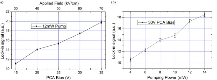
FIG. 2. Typical CW THz output power trends from a QD photomixer test device. (a) Monitored as the optical pump power is held constant and the PCA bias and accelerating E-field is increased; (b) as the PCA bias is held constant and the op-tical pump power is increased.
[image:3.612.53.417.631.765.2]Typical THz output power trends are exemplified in Figure2. It was found that the response from the bolometer increased predictably and repeatably as the PCA bias was increased from 15 V to 35 V, and likewise as the optical pump power was increased from 4 mW to 14 mW. The results displayed here correspond to a peak optical pump difference frequency of1.04 THz, which is well within the frequency limitations imposed by the expected carrier lifetime of
0.425 ps (s2:35 THz).
For further clarification of the ultrafast behaviour of the structure, the antenna was driven using a mode-locked Ti:Sapphire laser operating at 780 nm wavelength, with pulses of 150 fs duration at a repetition rate of 96 MHz. This pump beam was focused as before and the antenna bias and optical pump power were altered in the same way as the CW setup, and the THz output signal was monitored using the bolometer and LIA. An initial square-law dependence of the output signal on optical power and antenna bias was observed, after which (above 40 mW pump power) the struc-ture exhibited some output saturation behaviour, exemplified in Figure3, which is typically to be expected in an opera-tional PC THz antenna. The effective PC material in this case is the high-temperature-grown GaAs between the QD
layers, which on its own would not operate as an ultrafast PC switch due to the comparatively long carrier lifetimes. It is, therefore, likely that the inclusion of QD’s in this case has allowed the ultrafast carrier capture mechanism10 by which THz signals may be generated in the antenna. It fol-lows then that it is possible one may utilise the InAs QD’s themselves also as the PC medium. The photoluminescence (PL) spectrum for this structure is shown in Figure4, which indicates it could potentially allow for ultrafast photomixing processes to be generated using longer pump wavelengths approaching 1.3lm. Interestingly, coherent THz emission spectroscopy has observed THz signals from the structure as it is pumped by 150 fs pulses over a wavelength range of 650 nm to 1180 nm, and in addition to the detected THz out-put signal as the structure is pumped up to around 880 nm, the upper limit of the GaAs absorption, distinct THz emis-sion peaks were observed as the pump wavelength approaches the excited and second-excited state peak PL wavelengths of the InAs QD’s.18
[image:4.612.52.378.54.278.2]These results demonstrate the potential for increased opti-cal-to-THz efficiency offered by configurable QD-based photo-mixer structures over existing materials. The main advantages of these structures include the configurability of the PC region
[image:4.612.51.389.592.771.2]FIG. 3. Example THz output power trend observed as the structure is optically pumped by a Ti:Sapphire laser, operating at 780 nm with a pulsewidth of 150 fs. Initially, the square-law dependence of output power on optical pump power is observed, then the structure begins to exhibit THz output saturation characteristics.
to alter peak absorption wavelengths as well as photocarrier lifetimes and quantum gain by altering QD layer periodicity. Separate configuration of the PC region could allow the use of longer-wavelength QD-based pump sources, which are broadly tunable in their mean longitudinal wavelengths as well as dif-ference frequencies.5This opens up the potential for highly tun-able, ultra-compact, fully integrated, or on-chip CW THz transceivers similar to that presented, for example, in Ref.17as both the QD-based LD’s and photomixers operate around the same optical emission and pump wavelengths.
In conclusion, generation of continuous wave radiation was demonstrated, at a frequency of 1.04 THz from a semi-conductor optical heterodyne device, which comprises 40 periods of InAs quantum dot layers separated by 40 nm, with PC InGaAs wetting layers between GaAs capping layers. The photomixer was optically pumped by two spatially com-bined AlGaAs DFB LD’s at around 847 nm and 850 nm lon-gitudinal wavelengths.
This project was funded by EPSRC under Grant EP/ H015795/1. The authors would like to thank Dr D. Livshits of Innolume GmbH, Germany, for production of the QD photomixer structure. We would also like to thank: M2 Lasers, UK, for their part-funding support and provision of equipment; and Compugraphics, UK, for production of fine-feature photomasks, which made the production of sample antennas possible.
1
E. R. Brown, F. W. Smith, and K. A. McIntosh,J. Appl. Phys.73(3), 1480 (1993).
2R. Leyman, N. Bazieva, T. Kruczek, G. S. Sokolovskii, and E. U. Rafai-lov,Recent Pat. Signal Process.2(1), 12 (2012).
3D. H. Auston,Appl. Phys. Lett.26(3), 101 (1975). 4
L. Rui, C. M. Gu, L. R. He, W. Sen, W. Z. Shen, O. Hiroshi, and Q. X. Guo, Acta Phys. Sin.53(4), 1217 (2004).
5R. Leyman, D. I. Nikitichev, N. Bazieva, and E. U. Rafailov,Appl. Phys. Lett.99(17), 171107 (2011).
6
P. R. Smith, D. H. Auston, and M. C. Nuss,IEEE J. Quantum Electron. 24(2), 255 (1988).
7F. W. Smith, A. R. Calawa, C. L. Chen, M. J. Manfra, and L. J. Mahoney, IEEE Electron Device Lett.9(2), 77 (1988).
8
F. W. Smith, H. Q. Le, V. Diadiuk, M. A. Hollis, A. R. Calawa, S. Gupta, M. Frankel, D. R. Dykaar, G. A. Mourou, and T. Y. Hsiang,Appl. Phys. Lett.54(10), 890 (1989).
9A. R. Kovsh, N. N. Ledentsov, S. S. Mikhrin, A. E. Zhukov, D. A. Liv-shits, N. A. Maleev, M. V. Maximov, V. M. Ustinov, A. E. Gubenko, I. M. Gadjiev, E. L. Portnoi, J. S. Wang, J. Chi, D. Ouyang, D. Bimberg, and J. A. Lott, inPhysics and Simulation of Optoelectronic Devices XII, edited by M. Osinski, H. Amano, and F. Henneberger (Spie-Int Soc Optical Engineering, Bellingham, 2004), Vol. 5349, pp. 31.
10
E. U. Rafailov, S. J. White, A. A. Lagatsky, A. Miller, W. Sibbett, D. A. Livshits, A. E. Zhukov, and V. M. Ustinov,IEEE Photon. Technol. Lett. 16(11), 2439 (2004).
11
H. P. Porte, P. Uhd Jepsen, N. Daghestani, E. U. Rafailov, and D. Turchi-novich,Appl. Phys. Lett.94(26), 262104 (2009).
12M. C. Hoffmann, B. S. Monozon, D. Livshits, E. U. Rafailov, and D. Turchinovich,Appl. Phys. Lett.97(23), 231108 (2010).
13
D. Turchinovich, K. Pierz, and P. Uhd Jepsen,Phys. Status Solidi C0(5), 1556 (2003).
14C. Kadow, S. B. Fleischer, J. P. Ibbetson, J. E. Bowers, A. C. Gossard, J. W. Dong, and C. J. Palmstrom,Appl. Phys. Lett.75(22), 3548 (1999). 15
C. Kadow, A. W. Jackson, A. C. Gossard, J. E. Bowers, S. Matsuura, and G. A. Blake,Physica E7(1-2), 97 (2000).
16A. Klehr, J. Fricke, A. Knauer, G. Erbert, M. Walther, R. Wilk, M. Mikul-ics, and M. Koch,IEEE J. Sel. Top. Quantum Electron.14(2), 289 (2008). 17
D. Stanze, A. Deninger, A. Roggenbuck, S. Schindler, M. Schlak, and B. Sartorius,J. Infrared Millim. Terahertz Waves32(2), 225 (2011). 18G. Molis, A. Arlauskas, A. Krotkus, R. Leyman, N. Bazieva, and E. U.
Rafailov, in37th International Conference on Infrared, Millimeter, and Terahertz Waves, 2012. IRMMW-THz 2012 (Wollongong, Australia, 2012).