This content has been downloaded from IOPscience. Please scroll down to see the full text.
Download details:
IP Address: 123.231.126.183
This content was downloaded on 26/01/2017 at 12:02
Please note that terms and conditions apply.
Design, Fabrication and Demonstration of a 1x20 Multimode Interference Splitter for Parallel
Biosensing Applications
View the table of contents for this issue, or go to the journal homepage for more 2016 J. Phys.: Conf. Ser. 679 012027
(http://iopscience.iop.org/1742-6596/679/1/012027)
Design, Fabrication and Demonstration of a 1×20 Multimode
Interference Splitter for Parallel Biosensing Applications
*N Najeeb 1,3, Y Zhang 1, C J Mellor 2 and T M Benson3
1Department of Electrical and Electronic Engineering, University of Nottingham Ningbo China, 199 Taikang East Road, Ningbo, 315100, China.
2School of Physics and Astronomy, University of Nottingham, University Park, Nottingham NG7 2RD, UK
3
Department of Electrical and Electronic Engineering, University of Nottingham, University Park, Nottingham NG7 2RD, UK.
Abstract. This paper presents the experimental achievement of a silicon-on-insulator 120 MMI splitter andsimulation evaluations of the TE-like and TM-like mode MMI splitters for parallel biosensing applications. Device fabrication technology and optical characterisation results are provided.
1.Introduction
In 1973,OlofBrynghal used Fresnel image planes and a pinhole array to demonstrate the formation of multiple images of an object based on self-imaging techniques [1]. In 1975 R. Ulrich reviewed this phenomenon on multimode planer slab waveguides [2, 3] which was explained in more detail by Heaton et al. [4] in 1992. In 1995 Soldano and Pennings[5] stated the principle as “Self-imaging is a property of multimode waveguides by which an input field profile is reproduced in single or multiple images at periodic intervals along the propagation direction of the guide”.
Multimode Interference (MMI) devices are based on this self-imaging principle where the input image is reproduced into multiple images at the output with high uniformity [5]. Compared to Y-branches, MMI splitters can be made very compact and sharply increase tolerance to fabrication errors, as sharp edges near the branching points are avoided. MMI devices also have wide optical bandwidths, low cross talk and polarisation independence and are widely used in integrated optics as power splitters [6, 7], modulators [8], multiplexers [9], switches [10] and Mach-Zehnder interferometers [7].
1×N MMI splitters (where N is the number of outputs) have been theoretically and experimentally investigated widely especially for SOI based devices because of their compactness due to high index contrast, low losses, and compatibility with Si electronics and biological samples [11-16]. The highest number of outputs presented theoretically is 64 [17] and experimentally is 12 [13].This paper reports on the experimental achievement of 20 outputs.
space-out the MZI on the chip. For the device to work as an evanescent field sensor it should be designed to operate in TM polarisation mode to give enhanced sensitivity.
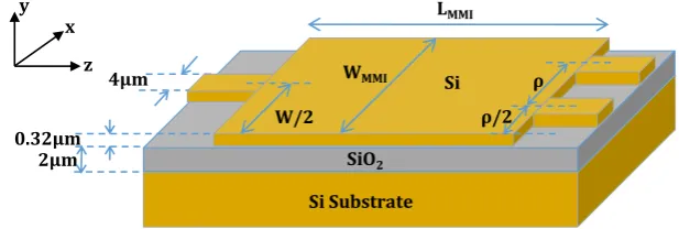
[image:3.595.141.450.189.293.2]2.Design of a MMI Device
Figure 1 shows the schematic diagram of a 1×2 MMI structure.
0.32µm 2µm
LMMI
Si Substrate SiO2
ρ
ρ/2 Si
WMMI
W/2 4µm
z
x
y
Figure 1: Schematic diagram of a1x2 MMI structure.
Inside the MMI cavity the beam is split into numerous modes and the symmetric intensity pattern is repeated periodically at the intervals of Λ along the guide:
𝛬 =𝑛𝑒𝑓𝑓𝑊𝑀𝑀𝐼
2
𝜆0 (1)
whereneffand WMMIare the effective refractive index and width of the MMI cavity respectively, and λ
0is the operating wavelength.
The N images formed are equally spaced across the multimode guide. The distance between the images is known as the Pitch, 𝜌 = 𝑊𝑀𝑀𝐼/𝑁. In the present work the pitch is fixed at 15µm to prevent interference between the output waveguides. WMMI is determined by the number of output waveguides,
N, where WMMI=Nρ.
Using these values the approximate MMI length, LMMI is calculated by Equation 2:
𝐿𝑀𝑀𝐼 =
𝛬 𝑁=
𝑛𝑒𝑓𝑓𝑊𝑀𝑀𝐼2
𝑁𝜆0 (2)
Equation 2 gives only an approximate length as the modes are not strictly confined to the multimode MMI region [15]. The optimum cavity length is found using a 3D BPM, and attained when the power of all the outputs isequal or almost the same. The MMI device has the lowest insertion loss and highest uniformity at this cavity length.
Figure 2 shows a 1×20 MMI simulated on RSoft Beam Prop. The waveguide width and height are kept at 4µm and 0.32µm respectively in this paper and theoperating wavelength is 1.55µm.
8th International Conference on Advanced Infocomm Technology (ICAIT 2015) IOP Publishing Journal of Physics: Conference Series 679 (2016) 012027 doi:10.1088/1742-6596/679/1/012027
Point at which all 20 outputs have the highest and equal power
[image:4.595.78.508.102.276.2]a) b)
Figure 2: Illustrating TE-like mode simulation for 1x2 MMI with a) longer cavity length and b) optimum cavity length.
3.Simulation Evaluation
3.1. Polarization Dependence
From Table 1 it can be seen that the optimum lengths for theTM-like mode is significantly shorter than for theTE-like mode making the device polarization sensitive. This is an advantage for evanescent field based biosensors which operate in TM-like mode to obtain high sensitivity.
Table 1: Optimum 1xN MMI cavity length for TE-like and TM-like modes.
N WMMI (µm)
LMMI calculated (µm)
LMMI Optimum (µm)
TE-like mode
TM-like mode
2 30 889.7 910.1 802.6
3 45 1334.5 1361.2 1200.4
5 75 2224.3 2269.7 2008.3
8 120 3558.9 3630.4 3205.1
12 180 5338.3 5443.4 4804.2
15 225 6672.9 6803.0 6006.2
20 300 8897.2 9063.5 8012.2
3.2. Insertion Loss and Uniformity
Insertion loss and uniformity are the two most commonly used Figures of Merits to compare the efficiency of MMI devices [19, 20]. Insertion loss is defined as:
𝐿𝑜𝑠𝑠 𝑖𝑛𝑠𝑒𝑟𝑡𝑖𝑜𝑛 𝑑𝐵 = −10𝑙𝑜𝑔10 𝑃𝑛 𝑃𝑖𝑛
𝑁
𝑛=1
(3)
where Pin is the input power and Pn is the power of the nth port.
The Non-uniformity is defined as:
[image:4.595.179.418.452.590.2]𝑁𝑜𝑛– 𝑢𝑛𝑖𝑓𝑜𝑟𝑚𝑖𝑡𝑦(𝑑𝐵) = −10𝑙𝑜𝑔10
𝑃𝑚𝑖𝑛
𝑃𝑚𝑎𝑥 (4)
wherePmin and Pmax are the maximum and minimum power observed in the N ports.
[image:5.595.174.426.225.355.2]Insertion loss and uniformity calculated for MMI splitters up to 120 are presented in Table 2.
Table 2: Insertion loss and Non-uniformity for 1×N MMIs.
N Insertion Loss (dB) Non-uniformity (dB) TE-like
mode
TM-like mode
TE-like mode
TM-like mode
2 0.11 0.07 0.00 0.00
3 0.12 0.12 0.00 0.00
5 0.16 0.17 0.01 0.01
8 0.19 0.28 0.02 0.01
12 0.21 0.40 0.04 0.03
15 0.23 0.49 0.04 0.03
20 0.23 0.73 0.06 0.08
In theory it is assumed that all guided waves are confined to the MMI cavity whereas in reality there will be leaky modes and radiation modes [4]. Therefore, losses increase as the MMI length increases when N increases [16].
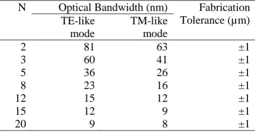
3.3. Optical Bandwidth and Fabrication Tolerance
The wavelength dependence or optical bandwidth is evaluated at the cost of a maximum additional loss of 1dB. Theoretically the optical bandwidth is inversely proportional to the number of outputs [21]. Fabrication tolerance is defined as the 1N MMI cavity width (WMMI) variation thatproduces an
additional loss of 1dB. Table 3 shows that the bandwidth reduces as the number of outputs increases, however, the fabrication tolerance stays the same.
Table 3: Bandwidth and Fabrication Tolerance for 1N MMIs.
N Optical Bandwidth (nm) Fabrication Tolerance (µm) TE-like
mode
TM-like mode
2 81 63 ±1
3 60 41 ±1
5 36 26 ±1
8 23 16 ±1
12 15 12 ±1
15 12 9 ±1
20 9 8 ±1
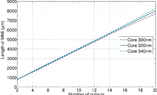
3.4. Wafer Core Thickness Tolerance
The core height of the SOI devices depends on the wafer purchased. The wafer used for this experiment has a standard deviation of 19.8 nm on a silicon core thickness of 320nm and buried oxide of 2µm. Therefore MMIs were designed to have +/- 20nm of silicon core height tolerance.
8th International Conference on Advanced Infocomm Technology (ICAIT 2015) IOP Publishing Journal of Physics: Conference Series 679 (2016) 012027 doi:10.1088/1742-6596/679/1/012027
[image:5.595.172.423.542.672.2]Figure 3 shows that the length of the MMI cavity increases linearly as the number of outputs increases; while the number of outputs increases, the tolerance for core thickness decreases.
Figure 3:Optimum MMI cavity length for silicon core thickness 0.32μm and +/-20nm for 1N MMI.
4.Device Fabrication
A 1×20 MMI was fabricated using photolithography and etch process as schematically illustrated in Figure 4. A commercially available SOI from SOITEC was used with a 0.32µm silicon layer on top of 2µm buried oxide layer.
The wafer was thoroughly cleaned by sonicating in solvents then dried with Nitrogen and dehydrated at 150°C for 30 minutes. Positive resist AZ6612 was spin coated at 4000rpm for 30 seconds to obtain a 1.2µm thick resist layer and soft baked at 110°C for 50 seconds. The resist was then patterned by exposing UV light for 6 seconds at 9mJ/s in a mask aligner (Karl Suss MJB-3). The exposed sample was developed for 30 seconds using AZ726MIF developer, rinsed with water and dried with nitrogen.
Positive resist layer
Si SiO2
Si a)
Positive mask
Si SiO2
Si b)
Si SiO2
Si c)
Si
SiO2
Si b)
[image:6.595.75.529.482.577.2]UV light
Figure 4: Schematic diagram of photolithography and etch process; a)Spin coating positive resist, b)UV exposure through a mask, c)Developed photoresist patterns and d)Etched silicon patterns.
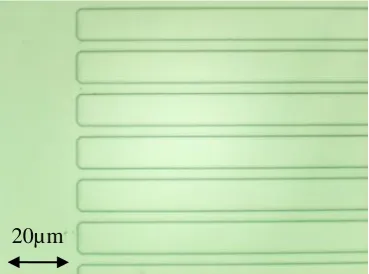
The silicon was etched for 110 seconds by inductively coupled plasma (ICP) etching using CORIAL 200L plasma etcher and the resist was removed with oxygen plasma for 105 seconds. In both processes the etching time included an extra 20 seconds to compensate for different etch rates at different point of the sample. This may result in etching in to the oxide layer slightly, but this will not affect the function of the product. Figure 5 shows the microscopic image of the outputs of an etched MMI.
Figure 5: Etched Si patterns of a 1×20 MMI coupler output waveguides(View from microscope x100).
Since the input waveguide has a cross section of 4µm by 0.32µm the coupling loss from an input tapered fibre to the Si waveguide would be high. To minimise the coupling loss, and more effectively couple light into the waveguide and out, a tapered SU-8 structure is used.SU-8 is an epoxy-based negative photoresist that contains eight epoxy groups per molecule giving the polymer very high functionality. Regions exposed to UV light polymerise resulting in an extremely high crosslink density [22] and a high degree of thermal stability. SU-8 has been used as optical waveguide in biosensing applications as it provides good transmission properties and low propagation loss [23-25]. The tapered SU-8 structure is 2µm in height and a width that tapers from 10µm to 4µm.
The SU-8 photolithography process as schematically illustrated in figure 6 was altered slightly from the standard protocol to prevent crack formation and poor adhesion between the resist and silicon.
1ml of resist per 25ml of substrate diameter was dispensed on to the surface of the etched sample. To obtain 2µm thick layer the SU-8 was spread at 500rpm for 5 seconds and Spin coated at 2000rpm for 30 seconds as shown in Figure. The sample was then soft baked at 65°C for 15 minutes and 95°C for 1 minute on two different hotplates. The sample needs to be gradually heated and cooled to room temperature to reduce thermal shock which causes the formation of waves on the surface of the resist. Leaving the sample overnight at room temperature helps drive out solvents and reduces the tackiness.
The resist was then exposed to UV light for 6 seconds at 9mJ/s as shown in figure. A post exposure bake was then done in a hotplate where the temperature was gradually increased from 65°C to 95°C during a time span of 20 minutes. The exposed resist cross links and harden during the post exposure bake. The temperature of the hotplate was gradually ramped down to 40°C and then the sample was removed from the hotplate and allowed to cool to room temperature.
Once the sample was cooled down it was developed with EC solvent for 40 seconds and then washed with Isopropanol and dried with Nitrogen to obtain tapered structures as shown in Figure 7.
To make the SU-8 mechanically and thermally stable a hard bake was incorporated into the process. The sample was hard baked in an oven where the temperature was gradually ramped up from 65°C to 175°C during a 35 minute time period and then allowed to cool naturally at room temperature.
20µm
8th International Conference on Advanced Infocomm Technology (ICAIT 2015) IOP Publishing Journal of Physics: Conference Series 679 (2016) 012027 doi:10.1088/1742-6596/679/1/012027
Si SiO2
Si SU-8 a)
Negative resist layer
b) UV light Negative mask
Si Si SiO2 SU-8
c)
SiO2 Si
Si 4-10µm
[image:8.595.79.509.109.230.2]2µm SU-8
Figure 6: Schematic diagram of SU-8 photolithography process a) 2µm thick SU-8 resist later spin coated, b) UV exposure over negative mask and c) Final structure with SU-8 on Si.
20µm
a) b)
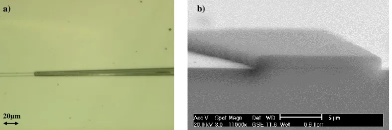
Figure 7:a) SU-8 taper well aligned with the waveguide (view from microscope x20) and b) Wafer cleaved through the SU-8(view from ESEM).
After fabrication the samples were cleaved perpendicular to the SU-8 tapers to obtain good quality end facets. A smooth facet is needed to minimise light scatter and maximise coupling efficiency. First a layer of positive resist was spin coated and soft baked for 30 seconds at 110°C in order to protect the device features. Two lines were scribed on either side of the tapered waveguide on a manual diamond scriber and then placed on a rubber mat with the sample features facing down. A small pressure was applied with a pen just enough to crack the wafer. Figure 7 b shows an ESEM image of a wafer cleaved smoothly through the SU-8.
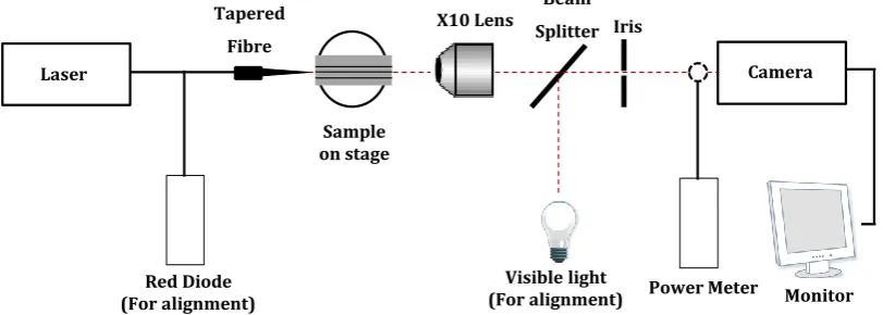
5.Experimental Characterisation Results
An optical bench set up was used as shown in figure 8 to evaluate the 1×20 MMI. A tuneable laser (Agilent 8164B Lightwave measurement system from 1465µm-1575µm) and a red diode was connected to a tapered fibre with a spot diameter of 2.5µm was used to couple light into the input SU-8 tapered waveguide of the MMI. A power meter was used to measure the light intensity of the light in front of the camera.
[image:8.595.91.485.292.423.2]Laser
Monitor Power Meter
Red Diode (For alignment)
Sample on stage
Camera
Visible light (For alignment) X10 Lens
Tapered Fibre
[image:9.595.97.503.105.250.2]Beam Splitter Iris
Figure 8: Schematic representation of Optical Bench set-up.
Figure 9 shows the successful operation of a 1×20 MMI splitter as seen from the infrared camera. It can be seen that the outputs are multimoded as expected.
6.Conclusion
A 120 MMI splitter has been designed, fabricated and tested in the lab. This device can be further improved by reducing the silicon core thickness from 0.32 µm to 0.22 µm which will greatly reduce the footprint of the MMI and will be more suitable for standard SOI fabrication. By using narrow single mode input and output waveguides and connecting N individual Mach-Zehnder interferometers to the outputs, this device can be used for evanescent field biosensing applications [18, 26].
7.References
[1] O. Bryngdahl, "Image formation using self-imaging techniques," J. Opt. Soc. Am., vol. 63, pp. 416-419, 1973.
[2] R. Ulrich, "Light-propagation and imaging in planar optical waveguides," Nouvelle Revue d'Optique, vol. 6, p. 253, 1975.
[3] R. Ulrich, "Image formation by phase coincidences in optical waveguides," Optics Communications, vol. 13, pp. 259-264, 1975.
[4] J. Heaton, R. Jenkins, D. Wight, J. Parker, J. Birbeck, and K. Hilton, "Novel 1‐to‐N way integrated optical beam splitters using symmetric mode mixing in GaAs/AlGaAs multimode waveguides," Applied Physics Letters, vol. 61, pp. 1754-1756, 1992.
[5] L. B. Soldano and E. C. M. Pennings, "Optical multi-mode interference devices based on self-imaging: principles and applications," Lightwave Technology, Journal of, vol. 13, pp. 615-627, 1995.
[6] D. S. Levy, P. Kyung Hyun, R. Scarmozzino, R. M. Osgood, C. Dries, P. Studenkov, et al., "Fabrication of ultracompact 3-dB 2 x 2 MMI power splitters," Photonics Technology Letters, IEEE, vol. 11, pp. 1009-1011, 1999.
Figure 9: Outputs of a 1×20 MMI splitter.
8th International Conference on Advanced Infocomm Technology (ICAIT 2015) IOP Publishing Journal of Physics: Conference Series 679 (2016) 012027 doi:10.1088/1742-6596/679/1/012027
[7] L. Zhuang, P. Wang, Z. Cao, G. Cao, Z. Wang, and F. Qiu, "A novel MMI–MZ all-optical switch," Optik - International Journal for Light and Electron Optics.
[8] P. Yue, B. M. Mao, X. Yi, Q. N. Li, and Z. J. Liu, "A MMI-based ultra-linear high-gain modulator and its performance analysis," Optics & Laser Technology, vol. 53, pp. 33-39, 2013. [9] M. R. Paiam and R. I. MacDonald, "A 12-channel phased-array wavelength multiplexer with
multimode interference couplers," Photonics Technology Letters, IEEE, vol. 10, pp. 241-243, 1998.
[10] W. Fan, Y. Jianyi, C. Limei, J. Xiaoqing, and W. Minghua, "Optical switch based on multimode interference coupler," Photonics Technology Letters, IEEE, vol. 18, pp. 421-423, 2006.
[11] A. Z. Chowdhury, "Performance study of silica-on-silicon based multimode interference (MMI) optical coupler," Photonic Sensors, pp. 1-9, 2013/06/07 2013.
[12] P. Trinh, S. Yegnanarayanan, F. Coppinger, and B. JalaIi, "Compact multimode interference couplers in silicon-on-insulator technology," in Lasers and Electro-Optics, 1997. CLEO'97., Summaries of Papers Presented at the Conference on, 1997, pp. 441-441.
[13] D. Kwong, Y. Zhang, A. Hosseini, Y. Liu, and R. T. Chen, "Demonstration of Rib Waveguide Based 1x12 Multimode Interference Optical Beam Splitter on Silicon-on-Insulator," in
Photonics Society Summer Topical Meeting Series, 2010 IEEE, 2010, pp. 221-222.
[14] A. Maese-Novo, R. Halir, S. Romero-García, D. Pérez-Galacho, L. Zavargo-Peche, A. Ortega-Moñux, et al., "Wavelength independent multimode interference coupler," Optics express, vol. 21, pp. 7033-7040, 2013.
[15] A. Cleary, S. Garcia-Blanco, A. Glidle, J. S. Aitchison, P. Laybourn, and J. M. Cooper, "An integrated fluorescence array as a platform for lab-on-a-chip technology using multimode interference splitters," Sensors Journal, IEEE, vol. 5, pp. 1315-1320, 2005.
[16] Q. Lai, M. Bachmann, and H. Melchior, "Low-loss 1× N multimode interference couplers with homogeneous output power distributions realised in silica on Si material," Electronics letters, vol. 33, pp. 1699-1700, 1997.
[17] T. Rasmussen, J. K. Rasmussen, and J. H. Povlsen, "Design and performance evaluation of 1-by-64 multimode interference power splitter for optical communications," Lightwave Technology, Journal of, vol. 13, pp. 2069-2074, 1995.
[18] N. Najeeb, Z. Yaping, C. Mellor, and T. Benson, "Photonic biosensor chip for early-stage cancer diagnosis," in Transparent Optical Networks (ICTON), 2015 17th International Conference on, 2015, pp. 1-4.
[19] R. Yin, J. Yang, X. Jiang, J. Li, and M. Wang, "Improved approach to low-loss and high-uniformity MMI devices," Optics Communications, vol. 181, pp. 317-321, 2000.
[20] Y. Shi, D. Dai, and S. He, "Improved performance of a silicon-on-insulator-based multimode interference coupler by using taper structures," Optics Communications, vol. 253, pp. 276-282, 2005.
[21] P. A. Besse, M. Bachmann, H. Melchior, L. B. Soldano, and M. K. Smit, "Optical bandwidth and fabrication tolerances of multimode interference couplers," Lightwave Technology, Journal of, vol. 12, pp. 1004-1009, 1994.
[22] Available: http://www.nanotech.dtu.dk
[23] D. Esinenco, S. Psoma, M. Kusko, A. Schneider, and R. Muller, "SU-8 micro-biosensor based on Mach-Zehnder interferometer," Rev. Adv. Mater. Sci, vol. 10, pp. 295-299, 2005.
[24] B. Shew, C. Kuo, Y. Huang, and Y. Tsai, "UV-LIGA interferometer biosensor based on the SU-8 optical waveguide," Sensors and Actuators A: Physical, vol. 120, pp. 383-389, 2005. [25] B. Y. Shew, Y. C. Cheng, and Y. H. Tsai, "Monolithic SU-8 micro-interferometer for
biochemical detections," Sensors and Actuators A: Physical, vol. 141, pp. 299-306, 2008. [26] Z. Yaping, "Multi-channelled waveguide chemical and biochemical optical sensing device,"
Patent, Great Britain Patent, 2010.