A New Two-Stage Voltage Source Inverter with Modulated DC-link Voltage and
Reduced Switching Losses
Christian Klumpner
University of NottinghamSchool of Electrical and Electronic Engineering Nottingham NG7 2RD
UNITED KINGDOM klumpner@ieee.org
Abstract – This paper proposes a new DC/AC power converter topology that is obtained by merging a buck type DC/DC converter and a DC/AC three-phase PWM Voltage Source Inverter (VSI) without the need of the passive components (smoothing inductor and capacitance) between the two stages. The novel topology is characterized by less hard switchings needed to synthesize the desired output voltage states, mostly because the average voltage seen by the VSI is modulated in such a way that enables the elimination of its zero voltage state and allows for some zero voltage switchings, reducing the switching losses, that makes this topology more suitable for higher frequency operation, which would ultimately reduce the size of the converter in applications where a load side output filter needs to be fitted.
I. INTRODUCTION
[image:1.612.373.510.366.460.2]The Voltage Source Inverter (Fig. 1a) supplied from a capacitive smoothed diode rectifier and operated with PWM are today's most common AC drive topology. Besides its well-known merits (simplicity, lowest number of semiconductors, good PWM waveform generation, good efficiency), it has also a few drawbacks: the need for bulky passive components with limited lifetime (DC-link electrolytic capacitors), a poor input current quality and rather high switching loss which in many application limit the potential for minimizing the size of filters needed to reduce the switching ripple. Other solutions based on an additional stage (boost of buck converter) as shown in Fig. 1b, placed between the constant voltage source and the inverter stage may improve the inverter stage efficiency (smaller switching voltage) as the DC-link voltage seen by the inversion stage continuously adjusts to the requirements but still involves additional passive components (boost inductances). However, the added buck converter stage will always experience hard switching and will always switch the full DC-link voltage but reduced current (constant power).
Fig. 1. Topologies of a DC/AC inverters: a) single stage buck VSI; b) two stage buck DC/DC and buck DC/AC VSI.
[image:1.612.49.301.609.708.2]This paper proposes the utilization of a buck type stage inserted between the DC-link capacitor and the VSI whilst eliminating the passive components that are normally required to connect the two stages: the inductance at the output of the buck converter and the capacitor at the DC-link side of the VSI, operating in a very similar way as a two-stage Direct Power Converter (DPC) [1]-[3]. The two two-stages, the buck converter and the VSI will not switch simultaneously, therefore the DC-link current is equal to one of the load phase currents for any given active VSI switching state. When the buck stage is supposed to switch, it will see as its load the AC motor having one phase connected in series to the other two phases paralleled, therefore, the condition for the buck converter to operate with a current source type load (inductive load) is accomplished.
Fig. 2. The topology of the proposed two-stage VSI operating with modulated average dc-link voltage seen by the VSI.
When the VSI is supposed to switch, the buck converter will connect the capacitor from the link to the VSI DC-link, therefore the fundamental condition for the VSI to operate with a constant voltage source type DC-link supply is accomplished. However, when the buck converter is in its freewheeling state, the VSI DC-link terminals need to be short-circuited and therefore return from an all transistor on switching state to any active voltage state is possible with only one hard switching of the buck stage, multiple zero voltage switching (ZVS) of the VSI stage being achievable.
In case the VSI operates in regenerative mode (Idc<0), the antiparallel diode of the buck transistor will provide a freewheeling path for the current to the diode rectifier capacitor, who's size needs to be determined in order to allow safe de-energizing of the load leakage inductance during an overcurrent protection triggered shutdown.
enables the elimination of zero-voltage switching states in the inversion stage due to a combined PWM-PAM and therefore, halving the number of hard switchings. Furthermore, because the switching pattern of the buck and inverter stages are synchronized, always except when Idc<0, one switching of the VSI will be a ZVS and therefore a further reduction of the switching losses is possible.
II. SPACE VECTOR MODULATION WITH MODULATED DC-LINK VOLTAGE AND ZERO
VOLTAGE STATE ELIMINATION
The SVM applied for a two level VSI utilizes a combination of two adjacent active voltage vectors and a zero-voltage vector to synthesize the reference voltage vector
Vout of variable amplitude and angle as requested by the load as illustrated in Fig. 3. The proportion between the duty-cycles of the two adjacent (active) voltage vectors V, V
gives its direction and the duty-cycle of the zero-vector relative to the switching period determines the magnitude of the reference voltage vector (1).
*
sin 3
U out
dm
d
m
U out*
sin
d
0
1
d d
(1) where mU is the modulation index and *out is the anglewithin the sector of the output voltage reference vector.
At maximum modulation index (mU =1), the VSI produces its maximum output voltage. The utilization of zero voltage states is still necessary in order to correct the amplitude of the voltage vector to follow a circle, otherwise its trajectory will follow an hexagon which means that the amplitude of the voltage vector will not be constant but will vary within a range of 1 to 1.15, the result being voltage distortion.
Fig. 4 shows the evolution of the duty-cycles of the active
switching states d, d and of the zero voltage state d0, which reaches zero in the middle of the sector. Actually, the duty-cycle of the zero voltage vector reflects the amount of dc-link voltage unused. Switching only between the two adjacent active voltage vector would require only two commutations per switching period, because within any sector, only one inverter output terminal changes state: for instance in the case considered in Fig. 3, =100 =101 therefore only phase C switches.
The necessity to correct the amplitude of the voltage vector by means of a zero voltage state needs at least other two commutations per switching period, which can be eliminated in case the dc-link voltage seen by the inversion stage can be adjusted accordingly. This means that when the VSI has to produce the maximum output voltage which normally happens at rated output power, by using a modulated DC-link voltage as given by (2), it is possible to cancel the zero voltage states in the inverter stage and therefore to reduce 50 % the number of hard switchings which finally will lead to the improvement in the efficiency of the VSI.:
ˆ
3
sin
sin
3
dc out
v
V
(2) Of course as a percentage, the reduction in switching losses is dependent also on the relative amplitude of the load current in the line that switches in order to produce the zero voltage state, which is normally dependent on the displacement angle between the load current and reference voltage vectors. The idea will be effective if the losses in the additional device that performs the modulation of the DC-link voltage according to (2) is smaller that the switching losses saved in the VSI.Table I illustrates the distribution of losses in a VSI feeding with full voltage (mU=1) an RL load (0.8 power factor), while controlled with different modulation schemes: sinusoidal PWM with two zero voltage vectors (ZVV), SVM with two and one ZVV and finally, SVM that uses only two active vectors while the DC-link voltage is modulated as in (2). The semiconductor parameters are given in Appendix A.
TABLE I
BREAKDOWN OF SEMICONDUCTOR LOSSES IN A VSI @10 kHz
Output power
Cond. loss
Switching loss
Sinusoidal PWM 5.46 kW 65.1 W 57.6 W (1.06 %) SVM 2 ZVV 5.53 kW 65.8 W 69.8 W (1.26 %) SVM 1 ZVV 5.54 kW 65.9 W 44.2 W (0.80 %) SVM modulated Vdc 5.34 kW 66.2 W 16.0 W (0.30 %)
It can be seen that savings of at least 0.5 % of the rated power are achievable. This may compensate for the additional losses in the buck stage connected in the intermediary link of a hybrid IMC (Fig. 2).
Fig. 5 shows the DC-link and output voltage waveforms for a VSI operating with modulated DC-link voltage as considered in Table I, while operating with unity modulation index.
001
011
110
010
V
V
V
out
*out
d
V
d
V
[image:2.612.85.263.61.185.2]100
101
[image:2.612.55.290.602.720.2]Fig. 3. The synthesis of the voltage reference space vector using the two adjacent active vectors.
Fig. 4. Variation of the duty-cycles with the angle within the sector when the modulation index is unity.
d d
Fig. 5. Voltage waveforms from a VSI operating with modulated DC-link voltage at unity modulation index: a) DC-link voltage; b) phase-to-neutral
voltage and its filtered value; c) line-to-line and its filtered value.
The most convenient way of modulating the DC-link voltage is to use a constant voltage supply and a switched mode power converter (i.e. the buck stage) to vary its amplitude. As the principle of Direct Power Conversion is applied here, the modulated DC-link voltage as presented in Fig. 5a will be synthesized by the buck stage as a succession of slices of the constant DC voltage source while its average over a cycle will follow the dependence given in (2). Therefore, it is necessary to synchronize the operation of the two stages in order to produce the same effects as in Fig. 5. The proposed switching pattern is shown in Fig. 6.
This technique can be used to vary smoothly the average over a cycle DC-link voltage seen by the inversion stage over a wide range, theoretically down to zero, which means that no zero voltage states will have to be synthesized by the VSI.
III. EVALUATION
Simulation models of the standard VSI and the proposed 2-stage-VSI have been implemented in PSIM. It can evaluate both the harmonic performance and estimate the conduction and switching losses [9]. In order to validate the proposed topology, an extensive evaluation is carried out including:
- Simulation results of a constant V/Hz ramp up;
- Comparison of the harmonic performance of a 400V normal VSI and proposed 2-stage VSI;
- Comparison of the semiconductor loss distribution in the normal and the proposed DC/AC topology in the situation of a medium voltage drive
- Experimental results with reduced input voltage from a prototype currently under development.
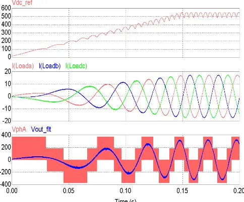
A. Simulation Results
Fig. 7 shows the result of ramping up the output voltage and frequency in a constant V/Hz way as appropriate for driving an AC motor, using the proposed topology and modulation technique. Fig. 7a shows the reference voltage that is set to be produced by the buck stage. Fig. 7b shows the resulting load currents, which prove to be balanced and sinusoidal, revealing that the modulation technique used is appropriate. Fig. 7c shows the PWM phase to load neutral voltage and its low pass filtered component (by means of an RC circuit). It is clear that a constant DC-link voltage is used, as there is no variable envelope for the PWM output voltage as shown in Fig. 5b and c.
B. PWM Harmonic Comparison
The FFT of the output line-to-line voltage of three different SVM pulse generation patterns are compared:
- single sided SVM for standard VSI (Fig. 8a):
00 = 4 hard switchings (last one=double) - double sided SVM for standard VSI (Fig. 8b):
00 = 4 hard switchings - single sided SVM for buck-VSI (Fig. 8c):
buck: 0Vdc0=2 hard switchings
INV: ; 1 hard switching (the other one=ZVS)
It is seen that lower switching harmonics are achieved when choosing a double-sided switching pattern at a similar number of hard switchings (however not same amount of losses as a different leg will perform one of them). Second observation is that identical spectrum of the output line-to-line spectrum can be obtained whilst using modulated dc-link with reduced number of hard switchings (3 compared to 4).
Buck
INV
0 VDC 0
[image:3.612.315.557.60.261.2]ZVS ZVS
Fig. 6 Switching states combination for the two-stage buck-VSI.
[image:3.612.59.294.423.507.2](a)
(b)
(c)
C. Semiconductor Losses Comparison
Before evaluating the results of the switching losses, it is necessary to look how the buck transistor is stressed during a switching period. The turn on and the turn off currents differ, depending on the inverter switching pattern and the load displacement factor. For example if the switching pattern is identical to the one shown in Fig. 6 and if =100 =101, the buck transistor will experience a turn on current equal to the current in phase A and a turn off current equal to the one in phase B. If the switching pattern of the inverter is swapped, the turn on current of the buck transistor will be the current in phase B and the turn off current, the current in load phase A. It is clear that it is therefore possible to minimize the switching losses by using the most convenient switching pattern that will minimize the current seen at turn-on because the switching losses associated with a hard-switched turn-on are typically 1.5- 3 times higher than the losses at turn off.
Fig. 9a shows the DC-link current seen by the buck converter as used in the simulations for evaluating the losses. In Fig. 9b and 9c, the turn on and turn off current are shown, making clear that in this particular situation the power circulates from the DC-link to the load and that the power factor of the load is 0.8 inductive, the switching stress during turn on is much smaller than during turn off.
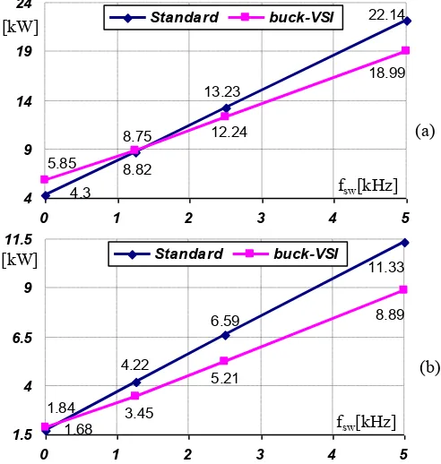
The loss distribution was implemented as in [7]-[9] for the standard and the proposed two-stage VSI. In order to justify the recommendation that this topology is best suited for medium and high voltage drives, a medium voltage DC/AC converter that would use 3.3 kV/800A state of the art devices was considered. The full list of circuit parameters as well as the parameters used in the loss models are given in Appendix B. It should be mentioned that the medium voltage IGBTs have slightly higher specific switching losses (3-6 times) than low voltage devices, which can be revealed by the so called turn-on and turn off loss times, whose definition is also given in Appendix B. If we compare this with the specific conduction losses (mainly ON-state voltage which increases only by a factor of 2), it will result a more convenient point where the two total semiconductor losses curves will overlap.
Fig. 10 shows the variation of the total semiconductor losses in the standard VSI and the proposed two-stage VSI in two situations, at high (0.95) and low (0.5) modulation index, in the condition that the load and the output frequency remain unchanged. The switching frequency where the two power loss curves overlap is 1.43 kHz. Below this value, the standard VSI has lower losses mainly because it has lower conduction losses (less devices in the current path). But because the rate of change of the switching losses for the two-stage VSI is smaller than the standard, it becomes more efficient at higher switching frequency, where additional benefits can be obtained such as smaller size of output LC filters, especially useful in UPS type applications.
[image:4.612.63.283.52.266.2]The frequency where the semiconductor losses overlap decreases a lot at low modulation index (300Hz), especially because the conduction losses of the buck transistor are
[image:4.612.319.565.436.695.2]Fig. 8. Output voltage FFT in three situations: a) VSI with single sided SVM; b) VSI with double sided SVM; c) buck&VSI SVM.
Fig. 9. Illustrating the stress that the buck transistor is subject to: a) The DC-link current; b) the turn-on current; c) the turn-off current.
(a)
(b)
(c)
(a)
11.33
4.22
1.68
6.59 8.89
1.84 3.45
5.21
1.5 4 6.5 9 11.5
0 1 2 3 4 5
Standard buck-VSI
fsw[kHz]
[kW]
22.14
13.23
4.3
8.75
18.99
12.24
5.85 8.82
4 9 14 19 24
0 1 2 3 4 5
Standard buck-VSI
fsw[kHz]
[kW]
Fig. 10. Comparison of the power losses vs. switching frequency for the standard VSI and the proposed buck-VSI a) at high modulation index: mU=
0.5, Iout-pk= 790Apk, PlossVSI=Ploss-2VSI @ 1430 Hz) and b) at low modulation
[image:4.612.63.299.583.716.2]dependent on the modulation index. This means that the two-stage VSI would be more efficient in applications where the load current (and torque for an AC motor drive) decreases as the modulation index and frequency for a constant V/Hz load, decrease (i.e. pumps and fans), which constitute the bulk of AC motor drive applications.
It should be noted that when performing a loss comparison using a low voltage (400V) and low power (kW range) model, an overlap frequency in the 10-30 kHz range results, which is not practical for an adjustable drive, which justifies the recommendation of using this idea in the medium/high voltage/power range where device switching behaviour is poorer.
D. Experimental Results
An experimental prototype has been constructed to demonstrate this technology. As it is still under development, only tests with reduced voltage (Vdc=120V) are available.
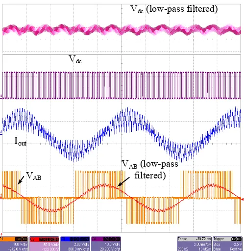
Fig. 11 shows the DC-link voltage seen by the inversion stage and the line-to-line output voltage VAB and below the
same waveforms magnified. The transition from one inverter leg commutating (left) to none of the A or B poles commutating (right) is clearly seen in the middle of the screen. In the left side, one of the inverter stage legs (A or B) is switching, while the third one (not shown) is continuously clamped to one of the DC-link terminals. In the right side of the screen this situation changes: because the DC-link voltage and the line-to-line output voltage VAB are identical,
it reveals that both outputs (A and B) are continuously clamped to a DC-link terminal (in fact, because the two voltages are not in opposition, it means that A=P and B = N), with only one inverter leg (not shown) switching.
Fig. 12 shows in its topside the DC-link voltage seen by the inverter stage and its low-pass filtered value, revealing clearly that it is modulated as described in section II. In the middle, the load current drawn by a resistive-inductive load is shown, revealing a peak current of the fundamental (excluding the switching ripple) of approx 2 A. The
switching current ripple is rather high, especially because the load inductance that has a filtering role is small. The line-to-line voltage and the low-pass filtered waveform is shown on the lower side of the figure, revealing that there is no notable low-order distortion present and that the proposed topology and modulation technique provides sinusoidal output voltage.
IV. CONCLUSIONS
A new two-stage DC/AC converter topology based on a two-stage arrangement with reduced switching losses is proposed. It has the same PWM voltage harmonics as a standard VSI but because it has a lower power loss gradient versus the switching frequency, it will prove more efficient at higher switching frequency were improvements in the converter power density (smaller filters and heatsinks) is expected. Estimation of the semiconductor losses for a medium voltage/power range DC/AC converter included in the paper predicts that the proposed topology may prove actually more efficient even at more usual switching frequency (300-1.5 kHz). Also, it is predicted that applications that operate heavily in the low modulation range, and also have a linear dependence between load current/torque with the modulation index/output frequency such as pumps and fans will be better off using the proposed two-stage VSI because the conduction losses, which are higher than for the standard VSI, are dependent on the modulation index.
V. ACKNOWLEDGMENT
Support for this work from the EPSRC is gratefully acknowledged (Grant EP/C52652X/1).
Vdc
Vdc
VAB VAB
[image:5.612.316.565.60.316.2]A and B continuous clamped
Fig. 11. DC-link and output line-to-line voltages of a buck-VSI. zoomed
Fig. 10. Filtered and actual DC-link voltage and the filtered and actual output line-to-line voltages of a buck-VSI.
Vdc (low-pass filtered)
Vdc
VAB (low-pass filtered)
VAB
Fig. 12. DC-link voltage seen by VSI, output current and filtered and actual output line-to-line voltages of a buck-VSI.
VAB (low-pass
filtered)
I
outVAB
[image:5.612.52.295.518.718.2]VI. APPENDIX A.
Device parameters for loss estimation in Table I: 1200 V/25A IGBTs and diode: VCE-0= 1.65 V, rd-IGBT= 75 m; VAK-0= 1.3 V, rd-FRD= 0.42 m; ton= 500 ns, toff= 222 ns.
VII. APPENDIX B.
Circuit parameters: Vdc= 1800V; Rload=1; Lload = 2.94
mH; fout = 40 Hz. Semiconductor parameters used in the loss
calculations: 3300V/800A ABB HipakTM device type
5SNE0800E330100; Conduction losses: IGBT: VCE-0=1.5V;
rd-IGBT=2.41m; Diode: VAK-0=1V; rd-FRD=2m
Switching: Eon@25oC =900mJ; Eon@125oC =1260mJ; Eoff@25oC
=950mJ; Eoff@125oC =1300mJ; ERR =1150mJ;
Definition of turn-on/off loss times:
@25 @125 2
2
3.16 1800 800
on C on C RR
on RR
on
CE C
E E E
E E
t s
V I V A
@25 @125
2
1.56
1800 800
off C off C
off off
CE C
E E
E
t s
V I V A
The conduction losses are modelled using:
0
0
1
( )
sim
T
cond IGBT CE d IGBT C C
sim
P V r I I dt
T
0
0
1
( )
sim
T
cond FRD AK d FRD K K
sim
P V r I I dt
T
The switching losses are modelled using:
0
1
2
sim
T
sw on CE on C on on
t sim
P
V
I
t
T
0
1
2
sim
T
sw off CE off C off off
t sim
P
V
I
t
T
VIII. REFERENCES
[1] J. Holtz, U. Boelkens, “Direct frequency converter with
sinusoidal line currents for variable speed ac motors”,
IEEE Trans. on IE, Vol. 36, No. 4, pp. 475-479, 1989. [2] G. Joos, N.R. Zargari, P.D. Ziogas, ”A new class of
current-controlled suppressed-link AC to AC frequency
changers”, Proc. of PESC '91, pp. 830 –837, 1991. [3] C. Klumpner, F. Blaabjerg, “Using Reverse Blocking
IGBTs in Power Converters”, IEEE Trans. on Industry
Application, Vol. 42, No. 3, pp. 807-816, 2006 issue. [4] N. Ravisekhar Raju, “A DC-link modulated three-phase
converter”, Proc.of IAS’01, Vol.4, pp. 2181-2185, 2001.
[5] N. Ravisekhar Raju, “Rippled DC Link Twelve-Pulse Converter with Sinusoidal AC Waveforms”, Proc. of IEEJ-IPEC 2005, paper 63p4, 2005.
[6] C. Klumpner, “A Hybrid Direct Power Converters with
Increased/Higher than Unity Voltage Transfer Ratio and Improved Robustness against Voltage Supply Disturbances”, Proc. of IEEE APEC’06, paper #10696, pp. 133-139, 2006.
[7] M. Bland, P. Wheeler, J. Clare, L. Empringham,
“Comparison of calculated and measured losses in direct
AC-AC converters”, Proc. of PESC’01, Vol. 2, pp.
1096-1101, 2001.
[8] F. Blaabjerg, J.K. Pedersen, U. Jaeger, “Evaluation of modern IGBT-modules for hard-switched AC/DC/AC
converters”, Proc. of IAS’95, Vol.2, pp. 997-1005, 1995.
[9] C. Klumpner, F. Blaabjerg, "Alternate ASDs: Loss Evaluation of Converter Topologies suited for Integrated Motor Drives", Industry Application Society Magazine, Vol. 13, No. 2, pp. 71-83, 2006.