Changes in Microstructure of Al/AlN Interface during Thermal Cycling
Yoshiyuki Nagatomo
1, Takeshi Kitahara
1, Toshiyuki Nagase
1,
Yoshirou Kuromitsu
1, Harini Sosiati
2and Noriyuki Kuwano
31
Central Research Institute, Mitsubishi Materials Corporation, Naka 311-0102, Japan 2High Voltage Electron Microscopy Laboratory, Kyushu University, Fukuoka 812-8580, Japan
3Art, Science and Technology Center for Cooperative Research, Kyushu University, Kasuga 816-8580, Japan
Changes in the microstructure of the interface between an Al layer and an AlN plate during thermal cycling was studied to clarify the fracture mechanism of the Al/AlN interface. Observation of the interface with an ultra-sonic flaw detector indicated that a crack was generated at an edge of the Al layer after approximately 2000 thermal cycles. Cross-section observation using SEM-AsB (Angle Selective Backscattered electron detector) revealed that the crack propagated into the Al layer and ran along the interface. The grain size of Al around the crack tip is 0.2– 1.0mm. This size is much smaller than that in the initial Al layer, which was approximately 500mm. It is considered that the refinement of Al grains was due to the accumulation of strains in the Al layer during the thermal cycling. Observations using SEM-AsB of higher magnification and TEM revealed that the crack was formed in the Al layer during thermal cycling, and propagated along the Al grain boundaries. SEM-EsB (Energy Selective Backscattered electron detector) image with a low accelerating voltage revealed that Si particles were precipitated in the Al layer during the thermal cycling. The Si particles were thought to be effective to hinder the progress of the refinement of Al grains.
[doi:10.2320/matertrans.MRA2008171]
(Received June 2, 2008; Accepted October 8, 2008; Published November 12, 2008)
Keywords: aluminum, aluminum nitride, interface, scanning electron microscopy (SEM)-electron backscattered diffraction (EBSD), scanning electron microscopy (SEM)-angle selective backscattered electron detector (AsB), scanning electron microscopy (SEM)-energy selective backscattered electron detector (EsB), transmission electron microscopy (TEM), fatigue fracture, precipitates
1. Introduction
Since AlN plates sintered with Y2O3additive have a good
insulating property and high thermal conductivity, they are used as circuit substrates for high power switching semi-conductor devices such as Insulated Gate Bipolar Transistor (IGBT). There are two kinds of circuit substrate using AlN plate: One is a Cu circuit substrate which is composed of Cu circuits joined to the both sides of an AlN plate, and the other is Al circuits substrate in which Al is used as a circuit material instead of Cu. The Cu circuit substrates have been used widely, because Cu has a good electric and a thermal conductivity. However, the Cu circuit substrates have a poor durability against crack generation in the AlN plate after thermal cycling. In order to overcome this problem, Al circuit substrates are now used for the applications with high-reliability required.1) The difference between the properties of Cu circuit substrates and Al circuit substrates during thermal cycling results from the difference in plastic deformation behavior of Cu and Al. The analysis by the finite element method (FEM) described that the plastic strain due to the difference between thermal expansion of the circuit metal and that of the AlN substrate causes more remarkable work-hardening in Cu in comparison with that in Al.2,3)
As mentioned above, the effectiveness of the Al circuit substrates in thermal cycle test has been verified by a system estimation and FEM analysis. However, few studies from the point of view of materials science were carried out to improve the reliability of Al circuit substrates. The purpose of this study is to clarify the fracture mechanism of the Al/AlN interface with investigating the changes in microstructure of the Al/AlN interface after the thermal cycling.
2. Experiments
2.1 Sample preparation
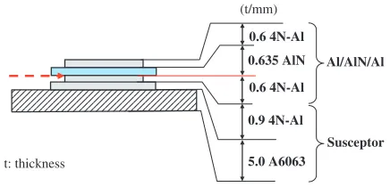
Figure 1 shows a schematic cross section of the specimen-set for a thermal cycle test. At first, rolled Al plates with 99.99% purity were brazed to both sides of AlN plate with Al-Si brazing sheets, under a vacuum of 103Pa at 922 K.
The dimensions of the Al plates (17mm29mm
0:6mmt) and the AlN plate (19mm31mm0:635mmt)
were decided to be a similar configuration to practical circuit substrates. The specimen-set for thermal cycle test was prepared with brazing the Al/AlN/Al component described above to Al Alloy (A6063) base plate. The base plate brazed to the Al/AlN/Al component enables to increase the load of the Al/AlN interface marked with the arrow in Fig. 1 and acceleration of fracture in the Al/AlN interface is expected. Before each thermal cycle test, the Al/AlN interface was examined with an ultra-sonic flaw detector to confirm no existence of defects.
0.6 4N-Al
0.6 4N-Al 0.635 AlN
0.9 4N-Al
5.0 A6063
(t/mm)
Al/AlN/Al
Susceptor
t: thickness
Fig. 1 Schematic image of a specimen-set for thermal cycle test. Cracks are expected near the interface marked with an arrow.
[image:1.595.318.536.395.500.2]2.2 Thermal cycling condition
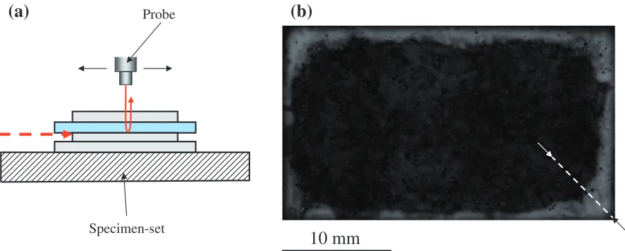
Thermal cycle test was carried out in two baths of Fluorinert that were controlled to be 233 K and 378 K. The specimen-set was soaked in each bath for 5 minutes alternately. The Al/AlN interface was examined for fracture propagation with an ultra-sonic flaw detector at every 1000 cycles.
2.3 Observation of microstructure
Field emission scanning electron microscopy (FE-SEM) and transmission electron microscopy (TEM) observations of the Al/AlN interface were carried out to analyze the fracture process during the thermal cycling. Specimens for FE-SEM observation were prepared by cutting the specimen-set with a diamond saw and polishing with an Ar ion beam mill to remove machining strains. In FE-SEM (S4300: Hitachi, Ltd. and Ultra 55: Carl Zeiss SMT), electron backscattered diffraction (EBSD: TSL) analysis and backscattered electron image observation were carried out. For the latter, an energy and angle selective detector (EsB and AsB, respectively) were used with changing the observation conditions such as accelerating voltage or working distance. Since diffraction contrast is emphasized in AsB images more than in conven-tional backscattered electron images, crystallographic infor-mation such as sub-grains or dislocations can be obtained.4) The specimens for TEM observation were prepared with a focused-ion-beam (FIB) mill (FB2000K: Hitachi Ltd.). In TEM (JEM-2000EX/T: JEOL) observation, the analysis by selected area electron diffraction, bright field image and dark field image were performed.
3. Results and Discussion
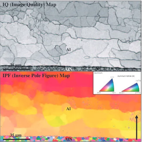
3.1 Microstructure of Al/AlN interface before fracture generating
Figure 2 shows an inverse pole figure (IPF) map obtained with EBSD analysis around Al/AlN interface before thermal cycling. It explains crystal-orientation of Al along normal direction of Al/AlN interface. It is revealed that h001iAl
directions of most Al grains were oriented in the normal direction of Al/AlN interface. The result is consistent to
the fact that cube-oriented grains are grown preferentially with a heat treatment in rolled Al with over 99.99% purity.5)
The grain size of cube-orientated Al was found to be approximately 0.6–1.0 mm. One cannot distinguish clearly a border between the Al brazed layer and pure Al by the difference in crystallographic-orientation. This suggests that the Al-Si brazing sheet once melted was solidified with an epitaxial relationship with the Al-plate having cube orientation.
Figure 3 shows an image quality (IQ) map and an IPF map around Al/AlN interface after 1000 cycles. It can be seen that the cube-oriented grains are divided into sub-grains (10– 50mm) by formation of sub-boundaries. The sub-grains have almost the same direction but with a slight twisting. This result explains that the Al layer is plastically deformed with the thermal cycling.
IPF (Inverse Pole Figure) Map
35µm
AlN Al
Al
AlN
Fig. 2 IPF map of Al/AlN interface before thermal cycle test. The arrow shows the direction to identify crystal-orientations of the Al layer.
35µm 35µm
IQ (Image Quality) Map
IPF (Inverse Pole Figure) Map
Al
Al
AlN
AlN
[image:2.595.70.523.73.247.2] [image:2.595.306.548.301.544.2]3.2 Fracture of Al/AlN interface with thermal cycling Figure 4 shows an ultra-sonic flaw image of the Al/AlN interface after thermal cycle test (4000 cycles). In this image, the brighter area indicates a propagating fracture. The fracture generated from an edge of Al after approximately 2000 cycles, and propagated to the center progressively. The propagation was faster at the corners of Al plate than that along the sides. It was considered that the faster propagation is attributable to a larger concentration of stress at the corner.
3.3 Cross sectional observation of Al/AlN interface after fracture generating
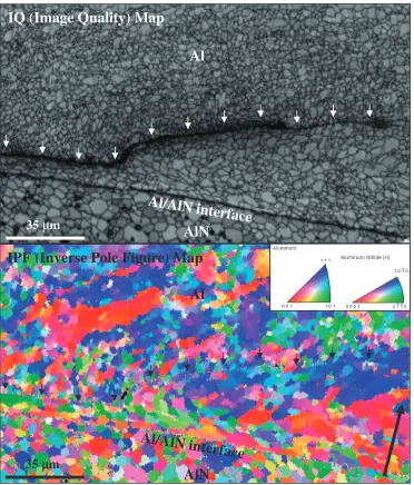
[image:3.595.307.545.323.497.2]Specimens for cross sectional SEM observation of the fracture area were prepared by cutting along the broken line remarked in Fig. 4, where the fracture propagation rate was expected to be faster. Figure 5 shows an AsB image of the specimen above-described and Fig. 6 shows an enlarged AsB image around the Al/AlN interface including a fracture termination. Brighter areas in Fig. 5 and Fig. 6 are of an Al layer. The arrows in Fig. 5 indicate a propagating fracture observed with an ultra-sonic flaw detector. It can be seen that a crack is running inside the Al layer at a distance of 10mmor less from the Al/AlN interface. Al grains are clearly observed in the Al layer thanks to diffraction contrast. It could be seen that Al grains had changed to be much smaller grain size of less than approximately 3mm. The decrease in the grain size of Al near the Al/AlN interface was especially remarkable and the fine-grained Al area reached approx-imately 100mmin width from the Al/AlN interface (Fig. 6). It was considered that the alternating plastic strains in Al layer were accumulated in the region near the Al/AlN interface, as explained with the FEM analysis (Fig. 7).
Figure 8 shows the IQ map and IPF map of EBSD analysis around a crack tip. It is revealed that the cube orientation disappeared in the grained Al region. In addition, fine-grains of Al close to the crack tend to have the crystal-orientation ofh111iAlin the direction of the arrow in Fig. 8. It
is considered that the shear strain due to the thermal cycling caused the alignment of {111}Alplane, which is the slip plane
of FCC structure. In the AsB image of higher magnification, it can be seen that the crack propagated along the grain boundaries in the fine-grained Al (Fig. 9). The Al grains at
10 mm
Probe
(a)
(b)
Specimen-set
Fig. 4 Observation of the Al/AlN interface with an ultrasonic flaw detector. (a): Schematic of observation condition and (b): Flaw image of the Al/AlN interface pointed with the arrow in (a). Specimen for cross-section observation was prepared with cutting along the broken line in (b).
100µm
AsB EHT:15.20kV
WD:4mm
AlN Al
100µm
Fig. 5 SEM-AsB image of Al/AlN interface after thermal cycle test. Arrows show the crack in Al layer.
AsB
AlN
Al
100µ m
20µm
EHT:17.00 kV WD:5 mm
[image:3.595.307.548.551.710.2]the crack tip reduced their size to be 0.2–1.0mm. The contrast in AsB images is similar to the diffraction contrast observed in TEM because AsB detected the backscattered electrons that are strongly related with channeling and diffraction. Figure 9 shows that the diffraction contrast caused by strain arising from dislocations and sub-grain boundaries can be found in the Al with AsB observation.
[image:4.595.48.289.74.247.2]It can be summarized that the refinement of Al grains proceeded with breaking the cube orientation as a result of accumulation of plastic strain. The size of refined grains reaches the order of sub-micrometer and the fracture proceeds along Al grains boundaries eventually.
Figure 10 shows an EsB image around the crack tip observed with a low accelerating voltage (2 kV). It can be seen that particles which have a brighter Z contrast than that of the Al matrix are precipitated in the Al layer. An EDX analysis revealed that an element of the particles consisted mainly of Si. Since the Si particles cannot be observed before the thermal cycle test, the Si particles are expected to be precipitated during the thermal cycling.
100 µm
4N-Al AlN
Al/AlN interface
A6063 4N-Al
AlN 4N-Al
Fig. 7 Result of FEM analysis of thermal cycle test. Contour shows distribution of plastic strains in Al layer after thermal cycling (3 cycles).
IPF (Inverse Pole Figure) Map
AlN
Al
Al/AlN interface
35
µ
m
AlN
Al
IQ (Image Quality) Map
35
µ
m
Al/AlN interface
[image:4.595.113.485.332.768.2]3.4 Mechanism of the crack propagation in Al/AlN interface
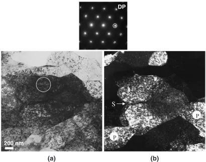
TEM observation of the microstructure near a crack in another specimen was carried out in order to investigate the mechanism of the refinement of Al grains and the crack propagation. Figure 11 shows the results of TEM observation of the Al near the crack prepared with FIB micro-sampling. Figures 11(a) and (b) show a bright field image and a dark field image obtained withhkl¼200diffraction spot, respec-tively. It can be seen that the sub-boundary was formed
laterally (inh100iAldirection of this grain) with dislocations
bundled in the grain. The grain was bruised at the right side pointed with the arrow of ‘‘S’’, and the grain was about to be divided into an upper and a lower parts. At the same time, the grains oriented in the almost same direction were connected from each other to become the laterally elongated grains as shown with ‘‘P’’. These results revealed that generation and accumulation of dislocations caused the refinement of Al grains. The accumulation of dislocations causes crack formation eventually.
EHT:17.00 kV WD:5 mm
400 nm
Crack front
Dislocation
Fig. 9 SEM-AsB image of tip of crack in Al layer. Al grains are observed clearly with diffraction contrast.
EHT: 2 kV WD: 3 mm EsB
2 µm
[image:5.595.307.548.71.240.2]Crack
Fig. 10 SEM-EsB image around the tip of a crack in the Al layer. Si particles are observed in the Al matrix with a Z contrast.
(a)
(b)
200 nm
DP
S
P
P
[image:5.595.49.289.71.241.2] [image:5.595.92.502.293.617.2]Figure 12 shows a TEM image of a crack tip near the Al/ AlN interface and diffraction patterns from region 1, 2 (Al layer) and 3 (AlN layer), respectively. The grain size near the crack tip is found to be approximately 1mmor less. The result agrees with that estimated from the AsB image of Fig. 9. The diffraction pattern revealed that grains in region 1 and 2 are aligned in almost the same direction but with a small twisting. The bright field image indicates that Al grains in region 1 are divided into grains by formation of sub-boundaries due to accumulation of dislocations.
Figure 136)shows variations of sub-grain size of Al with a repeated tension-compression test. It is found that the sub-grain size of Al decreases as the number of cycles increases. In addition, the grain size of Al around a fatigue crack tip after the repeated tension-compression test remained con-stant to be 1mmor less, despite a change of an alternating stress. The result supports that the formation of a crack in the Al layer is attributed to fatigue fracture. Because the fatigue crack in Al is formed when the grain size approach a critical size (1mm or less), pinning of dislocations with the Si particles in the Al layer observed in Fig. 10 would be effective to prevent the fatigue fracture by hindering the progress of the refinement of Al grains.
4. Conclusion
(1) Observation of the Al/AlN interface with an ultrasonic flaw detector indicated that a crack was generated at an edge of the aluminum layer after approximately 2000 thermal cycles.
(2) Cross-section observation using SEM-AsB revealed that a crack propagated into the Al layer and proceeded along the Al/AlN interface.
(3) The grain size of Al around the crack tip was 0.2– 1.0mm. This size is much smaller than that of approximately 500mmin the initial Al layer.
(4) It is considered that the refinement of Al grains is due to the accumulation of strains during the thermal cycling.
1
2
3
1
2
3
1
µ
m
Al
AlN
Crack
Fig. 12 Diffraction patterns and bright field image around the tip of crack in Al layer. Region 1 and 2 were Al layer. Region 3 was AlN layer.
Number of cycles σσf=12.7 MPa
20.6
24.5
0 1 2 3
Mean volume of sub-grains (
3
V/
µ
m)
Fig. 13 Variation of sub-grain size of Al with alternating stress (f) and
[image:6.595.312.541.428.628.2](5) Observations using SEM-AsB of higher magnification and TEM revealed that the sub-grain boundaries were formed in the aluminum layer during thermal cycling, and the crack propagated along the sub-grain bounda-ries.
(6) A SEM-EsB image with a low accelerating voltage revealed that Si particles were precipitated in the Al layer during the thermal cycling.
(7) Pinning of the dislocations with the Si particles would be effective to prevent the fatigue fracture by hindering the progress of the refinement of Al grains.
Acknowledgement
The authors express thanks to Dr. Takeshi Hanada
(Consult ZeroLoss Imaging Inc.) and Mr. Shigeaki Tachibana (SII NanoTechnology Inc.) for their cooperative SEM observation.
REFERENCES
1) T. Harada and Y. Baba: Proc. 15th Int. Conf. Electric Vehicles (EVS-15) (1998) CD-ROM.
2) Y. Nagatomo, T. Nagase and S. Shimamura: J. Japan Inst. Electron. Packag.3(2000) 330–334.
3) Y. Nagatomo and T. Nagase: Proc. 17th Int. Conf. Electric Vehicles (EVS-17) (2000) CD-ROM.
4) K. Shimizu, T. Mitani, S. Tachibana and H. Habazaki: J. Japan Inst. Light Metals56(2006) 454–458.
5) F. Seki and T. Kamijo: J. Japan Inst. Light Metals48(1998) 507–510. 6) S. Karashima:Strength of metals and alloys, (The Japan Institute of