Abstract - Computer vision and image processing continue to expand its area of application. Traditionally, this technology was hosted by a sequential processing paradigm of a Central Processing Unit (CPU). With this implementation in mind limits the usefulness of a device that is capable of parallel processing for several years. At the same time, it has been observed that common problem encountered when image processing routines are rendered on CPU is a slow processing rate.
This study presents the application of computer vision and image processing segmentation rendered on a Graphics Processing Unit (GPU), a parallel processing capable device, using CUDA developed by NVIDIA. It results to an impressive speed-up compared to the CPU. The study implements computer vision based quality inspection on pre-etched printed board fabricated by the Printed Circuit Board Prototyping Laboratory (PCBLab) of the University of San Carlos. The developed system can successfully detect defects such as open tracks, shorted tracks, neck form tracks, nick or mouse-bite form tracks, hole misalignment, and unwanted routes.
Index Terms – CUDA, GPU, image processing, quality inspection, execution time.
I. INTRODUCTION
N PCB fabrication process, etching is the most critical stage among all processes. It is important to determine the defects before etching so that no copper board will be waste. Thus, pre-etched quality inspection should be done properly to avoid this. However, current quality inspection in the PCB laboratory involves human interaction which was proven to be tedious, time-consuming and more importantly prone to error caused by tiredness and loss of concentration.
Manuscript received May 15, 2012; revised July 16, 2012. This work is supported in part by the Department of Science and Technology of the Philippines under the Engineering Research and Development Technology. Computer Vision and Image Segmentation Implemented on GPU Using Compute Unified Device Architecture as Applied on Quality Inspection of Pre-etched Printed Circuit board.
Philip Virgil B. Astillo is a faculty member from the Department of Computer Engineering of the University of San Carlos. His field of research is on machine vision and image processing. He finished his undergraduate and masters degree in the said university. (Email: [email protected])
Van B. Patiluna started his career as an instructor at the Department of Computer Engineering of the University of San Carlos. He had worked in several researches in robotics, microelectronics, machine vision and computer architecture. He finished his undergraduate and masters degree at the said university. (Email: [email protected])
Moreover, this method is prone to subjective evaluation of the quality of the PCB. This means that different inspectors may have different evaluations on the quality of a single PCB.
Computer vision based quality inspection could eliminate this problem. Several computer vision based quality inspection system has already been developed for this purpose. However, the processes involved are handled by a CPU. It had been observed for several years that the common problem encountered on CPU rendering in this kind of application is slow processing rate.
This study makes use the power of General Purpose GPU (GPGPU) in computer vision mainly on image processing routines using the Compute Unified Device Architecture (CUDA). This device is capable of parallel processing. Additionally, program codes for the image processing routines such as conversion from RGB to Gray Scale, Histogram Generation, Thresholding and Edge Detection were written rendering it to both the CPU and GPGPU. Execution time of both implementations was compared.
II. EXPERIMENTATION
A. Materials
The following materials were used in this study:
TABLE I LIST OF MATERIALS Microscope camera 90
90 mm x 180 mm PCB board USB Dongle Video Capture Card Desktop computer (dual-core) 3GB RAM
CUDA ready video card (16 cores, 512 MB dedicated RAM)
B. Procedure
There are two major sections in this study. First is the writing of two separate codes of the image processing routines that are important in this study for both CPU and GPU rendering. Furthermore, there were two types of memory mapping implementation for GPU rendering, namely global memory mapping and texture memory mapping. The execution time of the created codes between
Computer Vision and Image Segmentation
Implemented on GPU Using Compute Unified
Device Architecture as Applied on Quality
Inspection of Pre-etched Printed Circuit Board
Philip Virgil Astillo, Van Patiluna
the CPU implementation and GPU implementations were compared. 30 sample images were used to get the execution time of the written codes. Second is the development of an algorithm in detecting defects of a PCB that is concerned in this study. To test the reliability of the developed algorithms, 10 defective images for each type of defects were provided. Each of the 10 samples was tested 10 times.
Program codes of the image processing routines used in this research project were easily written for the CPU. Image conversion operations, for example gray scale image conversion was simply done by scanning the input image pixel-by-pixel and calculate the gray scale intensity value. Thresholding was done by traversing the gray scale image pixel-by-pixel and compared its intensity value to a threshold value. Histogram generation was done by traversing the whole image and pixel-by-pixel and flags its corresponding intensity bin.
These processes were translated for the GPU since all of it is parallelizable. Mapping an input image data into the GPU memory was one challenging factor in this study. Memory optimization is important area for performance. Another challenging factor is how to perform the operation into the GPU. Finding the appropriate and optimized creation of thread blocks and grid of blocks, which executes the created function or method called CUDA kernel, helps increase performance.
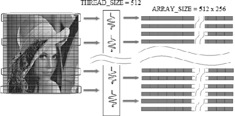
Image conversion was done by creating a number of threads equal to the total number of pixels of the resulting image. Each thread simultaneously converts the handled pixels. However, this way of creating threads is not applicable to histogram generation. Since CUDA thread works simultaneously, then one or more threads could access the same intensity bin that obviously result to bank conflicts. To avoid this issue, histogram generation was done by creating two kernels called one after the other as illustrated in figure 1 and 2.
Figure 1 illustrates the operation performed by the first kernel. A single block containing 512 CUDA threads is created and at the same time a bin with a dimension of 512 by 256 is allocated on the GPU memory. It follows that each thread holds one dimensional bin of a width of 256. This bin serves as a temporary storage of the frequency per intensity value. As show in the figure, each thread accesses a block of pixel from the source image traversing it pixel-by-pixel and gets the gray intensity value then flags its own corresponding bin. After this operation, the second kernel is called to get the resultant frequency.
To get the resultant frequency per intensity value, as shown in figure 2, 256 blocks of thread were created where each block contains 512 threads. A shared variable is allocated with a size similar to the THREAD_SIZE. This variable is accessible by all threads within the block. The process starts by copying the values generated from the first kernel into this shared memory. Notice that the values being copied in this shared variable are the temporary result frequency of a single intensity value generated from the first
kernel. After which, an algorithm called Parallel Thread Reduction, as shown in figure 2, was used to get the resultant frequency
The generated histogram is used to find the optimal threshold value. This value was used to separate the object of interest from the background when the binary image conversion operation was performed. The algorithm used to find the optimal threshold value is not parallelizable. A method was developed in this study to find the optimal threshold value.
However, the developed method assumes that the generated histogram is bimodal in shape or in other words, the generated histogram contains two valleys. Figure shows the process flow in finding the optimal threshold value.
These pre-processed mentioned above are important for the evaluation of the quality of the PCB. The evaluation starts by loading the template image or ideal design of the PCB into the developed system. After which, the test subject, which is just a small portion of the actual PCB board, was captured. The captured image undergoes the pre-processes in preparation for the defect detection stage.
[image:2.595.309.542.103.218.2]There were three different algorithms developed to detect the defects. To test the effectiveness of the developed Fig. 1. Kernel One Process Flow. Each thread accesses an assigned block of pixels and flags the corresponding intensity bin from its own bin.
[image:2.595.310.551.260.437.2]Fig. 3. Optimal Threshold Finding Process Flow. The algorithm searches the gray intensity value with the highest score in the two valleys. After determining these two values, the next operation is to find the gray intensity values with lowest score between the two highest score. The score refers to the number of pixels that a hold a specific intensity value.
algorithm properly, the coordinates of the captured image block is inputted into the system. To determine the location of the captured image, a two-dimensional grid lines is drawn on the template image and a guide is provided on the actual PCB board.
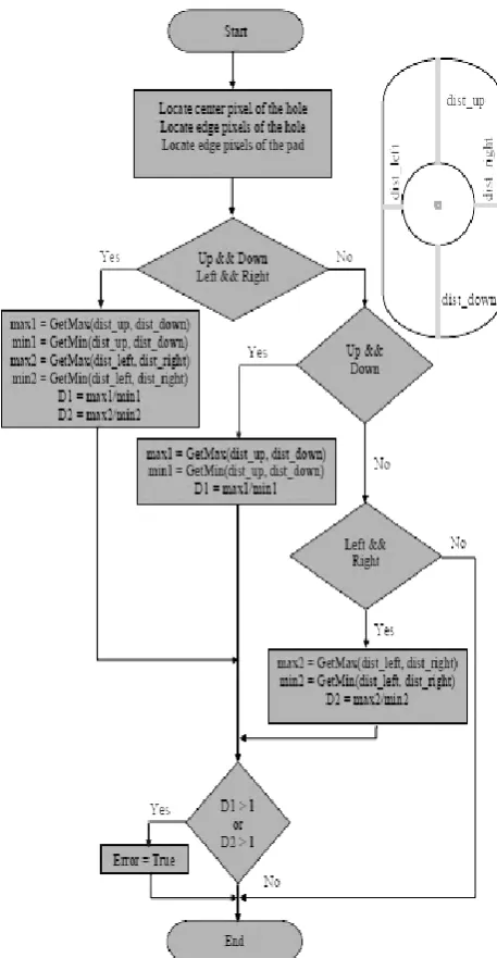
Figure 4 illustrates the developed algorithm in detecting the misaligned hole. To detect if a hole is misaligned, at least two opposite side of the edges of the pad should be present on the captured image. As shown in the figure, the algorithm starts by finding the center pixel of the hole. As shown in the figure, the algorithm starts by finding the center pixel of the hole. After which, the edge of the hole and pad is then determined. Through determining the distances from an edge of the hole to an edge of the pad from a four directions, hole misalignment can then be
determined. It is considered misaligned if the ratio between the maximum and minimum distance is greater than one. This condition is used because it indicates that the two distances are approximately equal which would mean that the center of the hole is very close to the center of the pad.
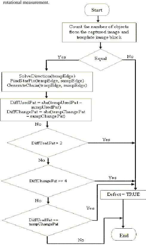
[image:3.595.311.540.116.557.2]Fig. 6. Neck and Nick Detection Algorithm. The developed algorithm implements pattern recognition. The generated patterns were analyzed and the conditions were set to notify that the captured image contains a defect.
Start
[image:4.595.115.231.168.264.2]End pattern generation is through the horizontal direction. Otherwise, the traversing direction is through the vertical direction. The starting coordinates serves as the reference point in generating or representing the connected pixel as chain of codes. The code is in numbering scheme shown in figure 6. The number code between two pixels is determined by simply calculating the rotational measurement. The generated patterns were then analyzed. If the set condition presented in the figure is satisfied, it would give a defect notification.
Another method was used to detect open circuit, short circuit and unwanted routes. The detection of these three
types of defect was simply done by counting the number of objects present in the sample image and its corresponding template image block. If the counted number objects between the two images are not equal, the system notifies that the captured image contains any of these three types.
III. RESULT AND DISCUSSION
The primary goal of this study was to make use of the power of GPGPU in computer vision mainly in image processing routines. At the same time apply quality inspection of pre-etched PCB by detecting defects. As such the gathered data can be classified into types, namely Performance Data and Detection Defect Effectiveness Test.
A. Performance Data
Execution time was gathered through time stamping. A time stamp function was inserted before and after the lines of code that performs a certain operation. Execution time of the 10 trials for each 30 sample images was tabulated and averaged. Average execution time per implementation was then calculated through the calculated average execution time of each 30 sample images.
Table III summarizes the time stamp result of the three implementations on performing RGB to Gray Scale Conversion, Histogram Generation, Gray Scale Image to Binary Image Conversion and Edge Detection. It shows the average execution time per implementation. Moreover, it shows the speed-up percentage between the three implementation of each operation.
Operation
Average Execution Time per Implementation
Percentage Speed-Up (Time1 vs Time2)
CPU GPUg GPUt
CPU vs
GPUg
CPU vs
GPUt
GPUg
vs
GPUt
Gray Scale
Conversion 1.66 1.32 1.12 20.18 32.63 15.60
Histogram
Generation 3.80 6.63 5.97 -42.69 -36.33 9.98
Binary Image Conversion
12.51 4.11 3.88 67.18 68.98 5.47
Edge
Detection 10.64 3.29 3.10 69.13 70.85 5.57
Figure 7 presents the execution time comparison between the three implementations of the said operations. It is observed in the figure that the three operations, namely Gray Scale Conversion, Binary Image Conversion, and Edge Detection, completed the execution faster when hosted by GPU using global memory mapping compared to CPU hosting. The speed-up percentage reaches up to 20.18%, 67.18% and 69.13%, respectively (Refer on Table II). Additionally, it is also observable that GPU hosting using texture memory mapping increases the speed. The improvement reaches up to 32.63%, 68.98%, 70.85%.
However on Histogram Generation, it is observed that CPU hosting finishes the execution in a shorter time Fig. 5. Direction for 8-directional chain code. The pattern of the
[image:4.595.42.287.300.711.2]connected pixel is represented using this numbering scheme. The code number between two pixels is determined through calculating the rotational measurement.
Table III
[image:4.595.303.552.469.610.2]compared to the GPU implementations. This caused a negative percentage as highlighted in Table II. This implies that the CPU hosting is 42.69% and 36.33% faster compared
to GPUg and GPUt, respectively. On the other hand,
comparing with each other the two GPU implementations, it appears the texture memory mapping is 9.98% faster than global memory mapping.
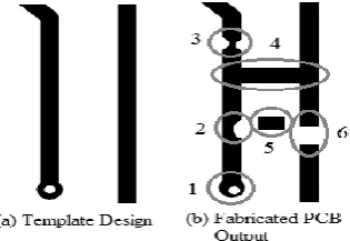
In this study, only six types of defect were taken into consideration, namely (1)hole misalignment, (2)nick or mouse-bite form track, (3)neck form track, (4)short circuit (5)unwanted route and (6)open circuit (Refer to figure 8). Each developed algorithms to detect a type of defect was first tested individually and then afterwards integrates them and test another set of sample image that are defective and non-defective.
Table IV summarizes the test result of the developed algorithm for detecting misaligned hole. It shows in the table that the algorithm could effectively detect the defect.
Table V and VI summarizes the result on testing the effectiveness of the developed algorithm to detect neck and nick type of defect. It shows from the tables that the success rate of detecting these types of defect is very high.
It is important to note that there was only one template design used to test the developed algorithm for these two typed of defects. This was because it was very difficult to simulate these types of defect on other templates since the tracks are very thin. It would result to open circuit when tried to simulate on other designs. The template design used to test has tracks with a width of 16 mils that is wide enough to form the defects.
Design Name Location Evaluation Success
Rate %
Row Column Pass Fail
PPS10 - 0010 22 22 10 0 100
PPS10 - 0010 16 16 10 0 100
PPS10 - 0010 12 15 10 0 100
PPS10 - 0010 10 16 10 0 100
PPS10 - 0010 13 17 10 0 100
PPS10 - 0010 05 24 10 0 100
PPS10 - 0010 05 15 10 0 100
PPS10 - 0010 21 28 10 0 100
PPS10 - 0010 13 24 10 0 100
PPS10 - 0010 12 34 10 0 100
Design Name Location Evaluation Success
Rate %
Row Column Pass Fail
PPS10 - 0010 18 33 10 0 100
PPS10 - 0010 19 22 10 0 100
PPS10 - 0010 04 30 10 0 100
PPS10 - 0010 09 35 9 1 90
PPS10 - 0010 05 20 10 0 100
PPS10 - 0010 05 34 10 0 100
PPS10 - 0010 07 34 10 0 100
PPS10 - 0010 12 22 10 0 100
PPS10 - 0010 08 16 10 0 100
PPS10 - 0010 02 16 10 0 100
Open circuit and short circuit defects are the most critical type of defect compared with the other in terms of its effect on the functionality of the board. It this defect would be present, the PC board would definitely be not functional. Though they are the most critical type, they can be easily detected.
Design Name Location Evaluation Success
Rate %
Row Column Pass Fail
PPS10 - 0010 18 33 10 0 100
PPS10 - 0010 19 22 10 0 100
PPS10 - 0010 04 30 10 0 100
PPS10 - 0010 09 35 10 0 100
PPS10 - 0010 05 20 10 0 100
PPS10 - 0010 05 34 10 0 100
PPS10 - 0010 07 34 10 0 100
PPS10 - 0010 12 22 10 0 100
PPS10 - 0010 08 16 10 0 100
PPS10 - 0010 02 16 10 0 100
Design Name Location Evaluation Success
Rate %
Row Column Pass Fail
PPS08 - 0016 21 07 10 0 100
PPS08 - 0016 09 42 10 0 100
PPS09 - 0016 04 06 10 0 100
PPS09 - 0016b 11 06 10 0 100
PPS09 - 0016 14 21 10 0 100
PPS08 - 0016 19 06 10 0 100
PPS09 - 0025b 11 06 10 0 100
PPS09 - 0016 03 06 10 0 100
PPS09 - 0016b 12 32 10 0 100
PPS09 - 0016b 15 09 10 0 100
CP U CP U CP U CP U GP Ug (g lo bal memo ry ) GP Ug (glo bal m em or y) GP Ug (glo bal m em or y) GP Ug (glo bal m em or y) GP Ut (t ex tu re m em or y) GP Ut (t ex tu re m em or y) GP Ut (t ex tu re m em or y) GP Ut (textu re memo ry ) 0.00 2.00 4.00 6.00 8.00 10.00 12.00 14.00 Gray Scale
Conversion GenerationHistogram Binary ImageConversion DetectionEdge
Av er ag e E xe cution T im e (m s)
[image:5.595.48.290.159.502.2]Fig. 7. Average Execution Time Comparison. This shows the comparison of the execution time between CPU hosting and GPU hosting. Gray Scale Conversion, Binary Image Conversion, and Edge Detection operations finishes a shorter time when handled by the GPU compared to the CPU.
Fig. 8. PCB Image. This shows the six types of defects concerned in this study.
Table IV
Hole Misalignment Detection Test Result
Table V
[image:5.595.308.550.267.538.2]Neck Form Detection Test Result
Table VI
[image:5.595.312.552.635.764.2]Nick Form Detection Test Result
Table VII
[image:5.595.91.249.658.766.2]Row Column PPS08-0016 20 27 NO PPS08-0016 14 26 NO
PPS08-0016 21 17 HM NN HM NN HM PPS08-0016 08 08 NO
PPS10-0010 14 31 NO PPS10-0010 14 34 NN PPS10-0010 16 20 NN
PPS09-0025b 19 5 OSU OSU NN OSU NN OSU NN OSU NN OSU NN PPS09-0025b 18 15 NO
PPS09-0025b 18 39 OSU OSU NN OSU NN OSU NN OSU NN OSU NN PPS08-0016 20 27 NO
PPS08-0016 14 26 NO PPS08-0016 21 17 HM
PPS08-0016 08 08 NO OSU OSU OSU OSU OSU OSU OSU OSU OSU OSU PPS10-0010 14 31 NO OSU OSU OSU OSU OSU OSU OSU OSU OSU OSU PPS10-0010 14 34 NN NN NN NN NN NN NN NN NN NN NN PPS10-0010 16 20 NN NN NN NN NN NN NN NN NN NN NN PPS09-0025b 19 5 OSU OSU NN OSU NN OSU NN OSU NN OSU NN PPS09-0025b 18 15 NO
PPS09-0025b 18 39 OSU OSU NN OSU NN OSU NN OSU NN OSU NN
HM NN
OSU NO
Evaluations
NO NO
NO NO
NO NO NO
Trial 6 Trial 7
NO Hole M isalignment Neck/Nick
Open/Short/Unwanted Route None NO NO
NO NO NO NO
Trial 8 Trial 9 Trial 10
NN NN NN NN OSU OSU OSU OSU HM HM
NO NO
NO NO NO NO NO
HM HM HM HM HM NO
Trial 3
NO NO OSU OSU NN NN NO NO
Trial 2
NO NO HM OSU OSU NN NN NO NO OSU OSU NN NN Design Name Location Error
Trial 1 Trial 4 Trial 5
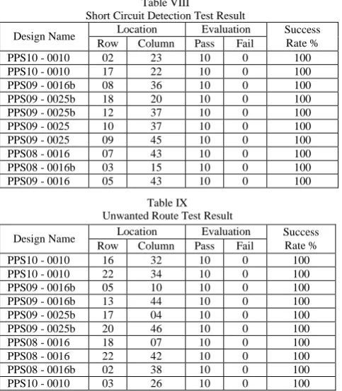
Table VII, VIII, and IX summarize the result of testing the effectiveness of the developed algorithm to defect open circuit, short circuit and unwanted route. It shows from the tables that the developed algorithm could effectively detect these types of error with a very high success rate.
After the individual testing, another set of samples that contains defective and non-defective PCBs were tested putting all the algorithms in active. It can be observed from Table X that system gave an evaluation of Neck or Mouse-bite type of defect on all trials of the first two sample images. However this erroneous evaluation can be explained for the fact that the sample image contains a track that is very thin which in the testing of Neck and Nick Algorithm
did not consider. The boundary of the tracks on both the template block and the resized sample image is adjacent to each other, thus will be considered as one object. It was out during this test that the algorithm used to detect neck and nick is successful if the boundaries of the tracks are distinct.
As for sample block 8 and 10, it was observed that in all trials the system two evaluations as shown in Table X. Though the error present is Open/Short/Unwanted Route, it is acceptable hat is will also give and evaluation of Neck/Nick since the patterns from template block and the resized sample image would definitely be unequal and would always violate the conditions set from on the Neck/Nick detection algorithm.
IV. CONCLUSION
The study makes use the power of GPU using CUDA to perform the image processing techniques mentioned above. Since CUDA thread work simultaneously, ideally it would finish or complete certain operation faster compared to CPU. However, it was discovered from the study that not all cases could speed-up an operation when rendered to GPU. Rendering an operation to the GPU would slow down execution time due to how a process is being parallelized and number of pixels in an image is being accessed or processed. It was discovered that GPU rendering is advantageous in terms of performance when high resolution images are involved.
Applying this technology on computer vision based quality inspection of pre-etched PCB with the developed algorithm to detect defects was successful. However since the developed system only scans a portion of the PCB done manually, the researcher recommends developing an automated scanning of the whole PCB.
ACKNOWLEDGEMENT
The researchers would like to express heartfelt gratitude and appreciation for the support to the PCB Laboratory Head, for giving the researchers a space to work on and their assistance provided whenever the researchers needs help.
REFERENCES
[1] Park, M., Jin, J., Au, S., Luo, S., and Cuit, Y., “Automated Defect Inspection System by Pattern Recognition”, International Journal of Signal Processing. Image Processing and Pattern Recognition, vol2. No.2, June 2009
[2] Heriansyah, R. Ibrahim, Z., Rahman al-Attas, S., Zabidi, M. and Aspar, Z., “PCB Inspection based-on Wavelet and Morphological
Image Processing Approaches”, Proceeding of the International
Conference of Robotic, Vision, Information, and Signal Processing, January 2003.
[3] Luo, Y. and Duraiswami, R., “Canny Edge Detection on NVIDIA CUDA”, Computer Vision and Pattern Recognition (CVPR) Workshop, pp. 1-8, 15 July 2008.
[4] Nadernejad, E., Sharifzadeh, S., Hassnpour, H., “Edge Detection Techniques: Evaluations and Comparisons, Applied Mathematical Science”, vol. 2 no. 2, pp. 1507-1520, 2008.
Design Name Location Evaluation Success
Rate %
Row Column Pass Fail
PPS10 - 0010 02 23 10 0 100
PPS10 - 0010 17 22 10 0 100
PPS09 - 0016b 08 36 10 0 100
PPS09 - 0025b 18 20 10 0 100
PPS09 - 0025b 12 37 10 0 100
PPS09 - 0025 10 37 10 0 100
PPS09 - 0025 09 45 10 0 100
PPS08 - 0016 07 43 10 0 100
PPS08 - 0016b 03 15 10 0 100
PPS09 - 0016 05 43 10 0 100
Design Name Location Evaluation Success
Rate %
Row Column Pass Fail
PPS10 - 0010 16 32 10 0 100
PPS10 - 0010 22 34 10 0 100
PPS09 - 0016b 05 10 10 0 100
PPS09 - 0016b 13 44 10 0 100
PPS09 - 0025b 17 04 10 0 100
PPS09 - 0025b 20 46 10 0 100
PPS08 - 0016 18 07 10 0 100
PPS08 - 0016 22 42 10 0 100
PPS08 - 0016b 02 38 10 0 100
[image:6.595.47.289.53.330.2]PPS10 - 0010 03 26 10 0 100
Table VIII
Short Circuit Detection Test Result
[image:6.595.47.292.422.673.2]Table IX Unwanted Route Test Result
Table X