21 August 2015
MASTER THESIS
AN EVALUATION OF THE
ADAPTEVA EPIPHANY
MANY-CORE
ARCHITECTURE
FINAL REPORT
Tom Vocke, BSc. (s0144002)
Faculty of Electrical Engineering, Mathematics and Computer Science (EEMCS)
Chair: Computer Architecture for Embedded Systems (CAES)
Graduation Committee: Dr.Ir. A.B.J. Kokkeler Ir. E. Molenkamp Ir. J. Scholten Ir. R. Marsman Ing. S.T. de Feber
Contents
Glossary 5
Abstract 6
1 Introduction 7
1.1 History and Motivation ... 7
1.2 Research Goals ... 8
1.2.1 Thesis Outline ... 9
2 Research Approach 11
2.1 Performance Analysis ... 11
2.2 Programming Model and Tool Support ... 12
2.3 Architecture ... 12
3 Relevant Background 13
3.1 Radar Processing and Beam-Forming ... 13
3.1.1 Channel Filtering: Hilbert and Bandpass Filter ... 14
3.1.2 Digital Beam-forming ... 14
3.1.3 Front-End Throughput and Processing Requirements ... 15
3.2 Epiphany Architecture ... 17
3.2.1 Memory Layout ... 17
3.2.2 eMesh Network-On-Chip ... 18
3.2.3 The Epiphany eCore ... 19
3.2.4 Maximizing Epiphany Performance ... 20
3.2.5 Initial E16G301 Performance Estimates ... 22
3.3 CRISP / Recore Xentium RFD Summary ... 23
3.3.1 Front-End Receiver Mapping and Performance ... 24
4 Benchmarking & Related Work 27
4.1 Related Work ... 27
4.1.1 eCore performance ... 27
4.1.2 eMesh Performance ... 29
4.1.3 eLink Performance ... 30
4.1.4 Epiphany Power Consumption ... 30
4.1.5 Remaining Work ... 31
4.2 Custom Micro-Benchmarks ... 32
4.2.1 Message Size vs. Bandwidth ... 32
4.2.2 eLink Bandwidth Sharing ... 32
4.2.3 eMesh Bandwidth Sharing ... 33
4.2.4 E16G301 Power Consumption ... 34
5 Micro-Benchmark Results 35
5.1.1 Message Size versus Bandwidth ... 36
5.1.2 eLink Bandwidth Sharing: ... 37
5.1.3 eMesh Bandwidth Sharing ... 39
5.1.4 E16G301 Power Consumption ... 40
CONTENTS Contents
6 Front-end Task Implementation 45
6.1.1 Hilbert Filter Optimization ... 45
6.1.2 Bandpass Filter Optimization ... 49
6.1.3 Beam-former Optimization ... 50
6.1.4 Task Power Consumption ... 52
6.1.5 Task Implementation Summary and Further Improvements ... 53
7 Front-End Receiver Design 55
7.1 Process Communication ... 55
7.2 Problem Decomposition ... 56
7.2.1 Filter Stage Decomposition ... 56
7.2.2 Beam-Former Decomposition ... 58
7.2.3 Load Balancing ... 58
7.3 Example Front-End Receiver Mapping ... 59
7.3.1 Load case and video sizes ... 59
7.3.2 Task Mapping on the E16G301 ... 59
7.3.3 Data Communication ... 61
7.3.4 E16G301 Front-End Receiver Performance ... 62
7.3.5 E16G301 Front-End Receiver Power Consumption ... 64
8 Tools and Architecture 65
8.1 Programming Model and Tool Support ... 65
8.1.1 Compiler ... 65
8.1.2 The Debugger and Instruction-Set Simulator ... 66
8.1.3 Performance Evaluation and Profiling ... 66
8.1.4 SDK Software Libraries ... 66
8.2 Architecture Design Choices ... 67
8.2.1 Reconfigurability ... 67
8.2.2 Dependability ... 67
8.2.3 Scalability ... 67
9 Conclusions and Future Work 69
9.1.1 Epiphany Architecture Performance ... 69
9.1.2 Programming Model and Tool Support ... 69
9.1.3 Architecture ... 70
9.1.4 Future Work ... 70
References 71
Appendix 73
A. Thales Many-Core Processor Survey ... 73
B. Power Measurement Load Cases ... 74
C. Power measurement setup ... 75
D. Software Implementation Details ... 77
Glossary
Term Meaning
MMAC(S) Million Multiply-ACcumulate operations (per Second) GFLOP(S) Giga (109) FLoating point OPerations (per Second) ADC Analog to Digital Converter
MPSoC Multi-Processor System-on-Chip FPGA Field Programmable Gate Array TDP Thermal Design Power
DMA Direct Memory Access MSB Most Significant Bit
KB / MB / GB Kilo (103), Mega (106) and Giga (109) Byte KiB / MiB / GiB Kibi (210), Mebi (220) and Gibi (230) Byte
FMADD Fused Multiply-Add (multiplies two arguments and adds the result to a third) MS/s Mega-Samples / second. A sample can be of arbitrary bit-length
VLIW Very Large Instruction Word RFD Reconfigurable Fabric Device GPP General Purpose Processor
GP_GPU General Purpose Graphics Processing Unit DRAM Dynamic Random Access Memory
eMesh On-Chip Network of the Epiphany Architecture eLink Off-Chip Link of the Epiphany Architecture
eCore Epiphany Processing Node
FPGA Field Programmable Gate Array SDK Software Development Kit FFT Fast Fourier Transform
Abstract
In this research we investigate the use of the Adapteva Epiphany Architecture, a modern many-core architecture, as a power efficient alternative to current signal processing solutions in phased-array radar systems. This research is performed using a E16G301 processor, which is a 16-core instantiation of the Epiphany architecture. Several micro-benchmarks are designed and performed to evaluate the processor, network and power performance of the E16G301. Based on the results of these micro-benchmarks a front-end receiver is implemented consisting of a Hilbert filter, a bandpass filter and a beam-former task.
The micro-benchmark results in chapter 5 show that it is difficult to achieve maximum performance for the on-chip and off-chip networks of the Epiphany architecture. For on-chip and off-chip communication only 1445MB/s out of 4.8GB/s and 306MB/s out of 600MB/s were achieved respectively. The low on-chip communication performance is partly caused by an errata item limiting the peak bandwidth to 2.4GB/s instead of 4.8GB/s.
The peak throughput achieved for the Hilbert filter is 53.1% of the theoretical peak performance, for the bandpass filter and beam-former this is 73.1% and 64.2% respectively. The measured power efficiency of are 14.35 GFLOPS/Watt for the Hilbert filter and 19.47 GFLOPS/Watt and 16.22 GFLOPS/Watt for the bandpass filter and beam-former respectively. It is expected that some performance gain is still possible through further optimization of the compiler generated code.
When mapping all the tasks on the E16G301 to form a front-end receiver chain, a sustainable input throughput of 34.4MS/s for four channels was achieved, forming 8 partial output beams for two sets of two input channels. This achieved a power efficiency of 15.8 GFLOPS/Watt, excluding off-chip communication and IO rail standby power.
INTRODUCTION 1 Introduction
1 Introduction
Radar systems have found many uses over the past decades. For some types of radar systems, such as air-surveillance systems, tracking of multiple possibly fast moving objects is desired. To achieve this, these systems typically use phased-array antenna's which support fast tracking, allow monitoring multiple directions simultaneously, and feature high antenna gain.
Phased-array antennas are made out of many smaller antenna elements. By applying a phase-shift to all individual antenna elements they can be made to sum constructively for signals coming from certain directions, and destructively for others. The process of applying the phase shifts to set the antenna radiation pattern is known as beam-forming, which can be done in both the analog and digital domain. When beam-forming is done in the digital domain, it is possible to form multiple beams simultaneously by applying different phase-shifts on the same set of data. However, digital beam-forming requires very large amounts of signal processing. Part of this processing is typically done very close to the antenna elements to reduce the bandwidth of the data that needs to be transported through the system. This introduces additional thermal and power constraints.
These large amounts of data and strict thermal constraints in phased-array radar systems require an efficient hardware solution. Currently this is mainly the domain of FPGA devices complemented by DSP processors, typically followed by of-the-shelf GPP/GP-GPU processing platforms. For a number of application domains, such as mobile radar systems, the current solutions are not always appropriate because of high power consumption, large development effort, and/or high component costs.
Recently, platforms with multiple processors and on-chip networks are rapidly gaining popularity. These Multiprocessor Systems-on-Chip (MPSoC) feature highly integrated hardware to offer a cost and energy efficient solution for the processing demands of an application. A special class of MPSoC are the many-core processors, which feature large numbers of processing cores to be able to fully exploit task level parallelism.
This thesis presents an evaluation of the Adapteva Epiphany Architecture [1], a recent many-core architecture, that could be a power efficient alternative to current solutions. The focus of this report is on the front-end radar processing stages, where power and processing requirements are most strict.
1.1 HISTORY AND MOTIVATION
Prior to this project, two large research projects have been conducted in cooperation with Thales, where, among other topics, the possibility of using many-core processors in high throughput streaming applications was investigated.
1. CRISP [2] (Cutting edge Reconfigurable IC's for Stream Processing, 2008-2011):
The CRISP project researched optimal utilization, efficient programming and dependability of reconfigurable many-cores for streaming applications.
INTRODUCTION 1.1 History and Motivation
During these projects a custom many-core platform was developed, called the Recore Xentium RFD. This platform was used to demonstrate the use of MPSoC in a scalable, dependable solution for stream processing. A beam-former application was implemented as a case-study.
The focus thus far has been mostly on scalability, reconfigurability and dependability properties of MPSoC. What remains to be investigated is how the raw performance and power efficiency of MPSoC systems will compare to that of current FPGA solutions. Although the Recore Xentium RFD could be used to research this further, it has a few limitations that introduce the desire to also look at other architectures. The most important are listed here:
• Precision: The Recore Xentium RFD excels at 16bit fixed point arithmetic, but lacks
floating-point performance. Future applications might require larger bit-widths or floating floating-point support.
• Performance: The silicon design was realized in a non-competitive (90 nm) technology [4],
limiting the clock speed and power efficiency.
• Programming Model and Tool Support: Software is currently hand-written using C and assembly. This might give an unrealistic view of the development effort required for many-core systems in general.
• Architecture: Currently, only the Recore Xentium RFD has been evaluated for the use in radar
systems. Researching a different architecture could provide more information on the important aspects of many-core architecture for this application.
A survey [5] of possible alternative architectures was made by Thales during the STARS project, of which the results are listed in appendix A (p.73). Here, the Adapteva Epiphany G4 shows the best power-efficiency of the processors listed, is tuned for 32bit floating point performance and features a C/C++ and OpenCL development environment. Unfortunately, the G4 was not available for purchase so instead the E16G301, a 16-core version of the same architecture, is used for the research.
1.2 RESEARCH GOALS
The goal of this research is to answer the following question:
“Can we use the Adapteva Epiphany Architecture as a power efficient alternative in the front-end processing chain of phased-array radar systems”
To answer this question, we will focus on three main topics for this research:
1. Performance:
◦ What throughput and power efficiency can be expected from the Epiphany Architecture?
◦ How does this throughput and power efficiency compare to existing systems?
2. Programming Model and Tool Support:
◦ How can we best develop software for the Epiphany architecture?
◦ What are the strengths and weaknesses of the provided development environment?
INTRODUCTION 1.2 Research Goals
1.2.1 Thesis Outline
To answer the questions stated above, first, the general approach taken in this research is presented in more detail and the relevant background information is given. This includes a description of beam-forming in general, the domain requirements and an overview of the Epiphany and Recore Xentium RFD architectures.
Next, related work is presented and several missing benchmarks are identified and implemented. The results of these benchmarks are discussed in chapter 5. In chapter 6, the design and optimization of several tasks typical for the front-end receiver chain are discussed.
Based on the micro-benchmark results, and the achieved performance of the individual front-end receiver tasks, a mapping of the front-end receiver on the E16G301 processor is presented. The design choices and performance numbers for this implementation can be found in chapter 7.
2 Research Approach
2.1 PERFORMANCE ANALYSIS
In order to evaluate the Epiphany architecture, first, the theoretical peak performance is determined. This is done based on the specifications provided by Adapteva, and will serve as a reference point throughout this research. After this, the maximum achievable throughput and power efficiency of the Epiphany architecture are evaluated on the E16G301.
The main goal of evaluating this performance is to allow for a comparison to existing solutions. Comparing performance of computing systems is typically done using industry standard benchmarks. These benchmarks can be roughly divided into two classes:
• Micro Benchmarks: Specifically tuned software is used to test individual features or components of a system. For instance, a program with specific memory access patterns can be used to test cache performance. Micro benchmarks are typically used for verifying and tuning the performance of separate system components.
• Application Benchmarks: A set of full applications or application kernels is used to test the
overall system performance. For an application benchmark to be useful, it is very important that it is representative of the desired application domain, and that it is implemented in a similar way to how the real-world application would be implemented [6].
For this research, first, several micro-benchmarks will be built to estimate the achievable percentage of the peak performance presented by Adapteva for real-world applications. These benchmarks will focus on the performance and power efficiency of the on-chip network, off-chip network and individual processor components separately. The details of related research, and the design of these benchmarks are presented in chapter 4.
Actual application performance will depend on many factors such as partitioning, scheduling, memory requirements, data-dependencies and compiler efficiency. It is not uncommon to only achieve small fractions of peak performance for real-world applications, as shown in [7] where for a 2D-Fast Fourier Transform (FFT) application, only 13% of peak performance on the Epiphany architecture is achieved, versus 85% of peak performance for a matrix multiplication problem. This means the result of the micro-benchmarks alone will not say much about the overall performance of an application.
For a good estimate of the achievable throughput a suitable application benchmark is required that can be run on all the platforms that are to be compared. Implementing new software on the Recore Xentium RFD and other platforms will be very time consuming and outside the scope of this research, therefore this research will focus on applications that have already been implemented. One case that is often used to represent the front-end radar processing domain, and has been implemented on both the Recore Xentium RFD and other platforms, is the front-end receiver, consisting of channel filters and a digital beam-former [8].
RESEARCH APPROACH 2.2 Programming Model and Tool Support
2.2 PROGRAMMING MODEL AND TOOL SUPPORT
The following paragraph is taken from [1], and describes the programming model for the Epiphany architecture as presented by Adapteva:
“The Epiphany architecture is programming-model neutral and compatible with most popular parallel-programming methods, including Single Instruction Multiple Data (SIMD), Single Program Multiple Data (SPMD), Host-Slave programming, Multiple Instruction Multiple Data (MIMD), static and dynamic dataflow, systolic array, shared-memory multi-threading, message-passing, and communicating sequential processes (CSP)”
Essentially this says; anything is possible. It is left to the programmer to determine what best suits the need for the desired application. In this research we will investigate the advantages and disadvantages of several of the mentioned design approaches to determine what can be best used for the digital beam-former in chapter 7.
Adapteva provides an Eclipse C/C++ based development environment. Alternatively, Brown Deer technology provides an OpenCL environment with Epiphany architecture support. In this research, only the C/C++ based environment will be used since the Brown-Deer environment uses the libraries and compiler of the official Adapteva SDK in the background, and will therefore not likely introduce any performance benefits.
2.3 ARCHITECTURE
During the STARS and CRISP project, less tangible properties of a system such as scalability, reconfigurability and dependability were investigated. These properties are important in real-world solutions where products need to be verifiable, are used for multiple products for cost reasons, and need to be relied upon in critical systems.
In [9], the definitions of a few key properties are presented, which are summarized below:
• Reconfigurability: The ability of a system to change its behaviour at design or run-time by
changing hardware and/or software configurations.
• Dependability: This describes the trustworthiness of a system. It consists of both health monitoring capabilities and robustness of the design.
• Scalability: The ability of a system to handle growing amounts of work gracefully or its ability to be enlarged to accommodate that growth.
3 Relevant Background
In this chapter the application domain and Epiphany architecture are introduced to better understand the relevance of some of the topics discussed in this research. First, the basic concepts of phased-array radar systems, beam-forming and their typical requirements are introduced. Then an overview of the Epiphany architecture is presented. A more detailed description of the Epiphany architecture can be found in the Epiphany architecture reference [1].
3.1 RADAR PROCESSING AND BEAM-FORMING
The processing requirements in radar systems depend strongly on the application. In [9], an overview is given of several common radar applications and their processing needs. The processing solutions for these systems are divided into a transmit and a receive chain. This research will focus on the front-end processing stages in the receive chain of a radar, throughput and processing requirements are most strict.
[image:13.595.75.486.368.574.2]Figure 1 shows an overview of a typical phased-array radar receiver processing setup. Here each antenna element is connected to a transmit-receive module that filters and mixes the antenna signal to an intermediate frequency in the analog domain. These modules also convert the resulting signals to the digital domain. The digital streams are sent to the processing front-end, where channel filtering is applied and beam-forming is done. The resulting beams are sent to the processing back-end where algorithms for detection, extraction, classification and tracking are implemented [9].
Figure 1: Phased-array antenna receive chain processing overview [9]
T/R Module
… .
T/R Module
T/R Module
Front
End
Antenna
Elements ChannelsDigital Antenna Beams
Back
End
Tracks
Comms
RELEVANT BACKGROUND 3.1 Radar Processing and Beam-Forming
3.1.1 Channel Filtering: Hilbert and Bandpass Filter
The first step of the digital channel filtering in the front-end is to transform the real-valued sample streams from the transmit-receive modules into complex representations using the Hilbert transform [10]. Complex-valued samples offer more convenient access to important signal characteristics such as instantaneous amplitude, phase and frequency. After the Hilbert filter, a bandpass filter is applied to select the desired frequency band and equalize small differences in the individual antenna elements. A decimation factor can applied in both filter stages, meaning all input samples are used for the filter operation, but only part of the output samples are computed. Decimation decreases the filter output rate, thereby decreasing the filter processing requirements while preserving more information of the original signal in the output signal than would be achieved if the sample-rate were simply reduced. On the Recore Xentium RFD, both the Hilbert and the bandpass filter are implemented through direct-form convolution. Efficient FFT based convolution algorithms exist [11], however, additional memory is required for the storage of intermediate frequency domain signals and for small signals lengths, the performance gain is minimal. Since memory is limited on the Epiphany, the extra FFT memory footprint is undesirable. Also decimation will likely result in a relatively small amount of samples to process. For these reasons a direct-form convolution approach is used in this research, similar to the Recore Xentium RFD implementation.
3.1.2 Digital Beam-forming
The beam-forming stage is responsible for introducing the desired phase-shifts for phased-array operation, and for summing all the antenna output channels to form the beam output. The phase-shifts can be applied independently to all channels and the ordering of summation does not matter. This allows concurrent processing of the workload by dividing the channels, and splitting up the channel summation in multiple stages. An example of this is shown in Figure 2.
The beam-former works on a complex valued input stream. Equations (1) and (2) show that multiplying
Figure 2: Beam-former variations. Left: Single process adds all channels.
Right: Summation is spread over two stages, three processes
s
1(t)
s
2(t)
s
3(t)
s
4(t)
+
s(t)
s
1(t)
s
2(t)
+
s(t)
+
s
3(t)
s
4(t)
+
Θ
1Θ
2Θ
3Θ
4Θ
1Θ
2Θ
3Θ
4 Phase-shiftersInput Signals
RELEVANT BACKGROUND 3.1 Radar Processing and Beam-Forming
z
1=
r
1⋅
e
j⋅φ1⋮⋮
z
2
=
r
2⋅
e
j⋅φ2 (1)
z
1⋅
z
2=
r
1⋅
e
j⋅φ1
⋅
r
2⋅
e
j⋅φ2
=
r
1
⋅
r
2⋅
e
j⋅(φ1+φ2) (2)
3.1.3 Front-End Throughput and Processing Requirements
In [9], the processing requirements are specified in terms of throughput and the number of required operations per task. Although the requirements for the front-end processing differ strongly between applications, all the receive chains perform the same tasks. The requirements for a specific application depend on the input sample rate (FS), the number of input channels (NC), the filter decimation factors
(DHF, DBPF) the number of filter taps (NT) and the number of output beams (NB). For both the throughput
and processing requirements a relation between the above parameters and the requirement can be determined.
Throughput Requirements
The throughput requirements per task depend on the output rate of the preceding task, as shown graphically in Figure 3. Here HF and BPF are the Hilbert and bandpass filter respectively, and BF denotes the beam-former stage. The output throughput of each task can differ from the input throughput depending on filter decimation factors and the number of beams that are formed. The throughput requirements between all tasks scale linearly with the input sample rate.
Processing Requirements
The processing requirements per task depend on the required throughput per task, and the number of operations required to process each sample for a given task. In [9], some estimates are made on the processing requirements based on a direct-form 32 tap FIR filter implementation of the filters. These
Figure 3: Throughput requirements per tasks in the front-end receiver processing chain. (HF=Hilbert filter, BPF=Bandpass filter, BF=Beam-Former, BE=Back-end)
ADC HF BPF
BF
BE
CH1
... CH2
... CHn
F-sample (real)
ADC-rate / Decimation (complex)
HF-rate / Decimation
(complex)
#Beams
x BPF-rate
RELEVANT BACKGROUND 3.1 Radar Processing and Beam-Forming
• Complex Multiply(MCMUL): 4 (multiply) + 2 (add) = 4 MACs
• Complex Add (MCADD): 2 (add) = 2 MACs
• Complex Multiply Accumulate (MCMAC): 4 (multiply), 4(add) = 4 MACs
• Hilbert Filter FIR tap (MHF_FIR): 2 (multiply) + 2(add) = 2 MACs
• Bandpass Filter FIR tap (MBPF_FIR): 1 (CMAC) = 4 MACs
Based on the costs of these operations, the processing costs per task can be defined. This is done in equations (3), (4) and (5) where CHF CBPF and CBF denote the number of MACs required for each task,
the MHF_FIR, MBPF_FIR and MCMAC terms represent the number of MACs requires for a specific operation,
and NT is the number of filter taps.
C
HF=
N
C⋅
F
SD
HF⋅
N
T⋅
M
HF FIR (3)C
BPF=
N
C⋅
F
SD
HF⋅
D
BPF⋅
N
T⋅
M
BPF FIR (4)C
BF=
N
C⋅
F
SD
HF⋅
D
BPF⋅
N
B⋅
M
CMAC (5)Note that the Hilbert filter and Bandpass filter implementations differ in processing costs since the Hilbert filter operates on a real-valued input stream, and the bandpass filter operates on a complex input stream as shown in Figure 3.
RELEVANT BACKGROUND 3.2 Epiphany Architecture
3.2 EPIPHANY ARCHITECTURE
The Epiphany architecture is a recent many-core architecture design by Adapteva aiming at power efficiency. It features a homogeneous grid of processing nodes, known as mesh-nodes, connected by a Network-on-Chip (NoC). Each node consists of a processor core, local memory, a network interface and a DMA engine. For this research a 16-node variant called the E16G301 is used, which comes on a small computer board called the Adapteva Parallella [12].
The Parallella uses a Xilinx Zync 7000 series device which contains two hardware ARM processors, several peripherals and some FPGA fabric. The FPGA is used to instantiate a link to the E16G301 processor. An overview of this board and the E16G301 is given in Figure 4.
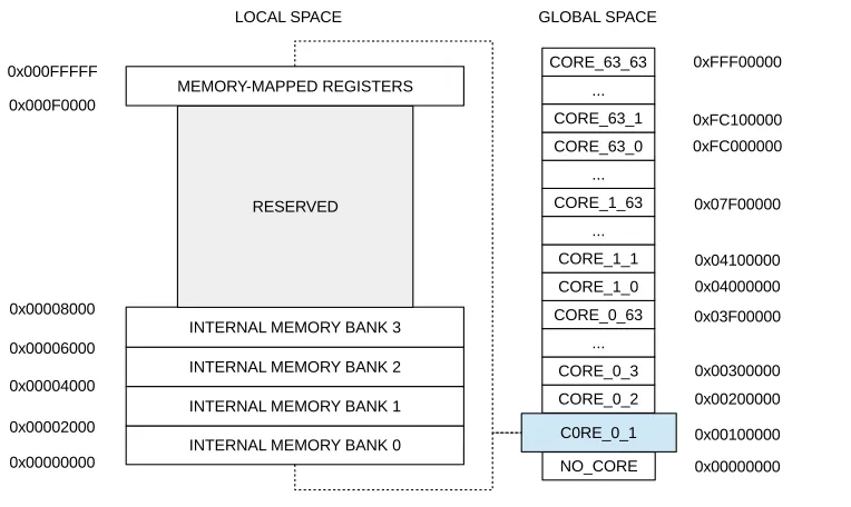
3.2.1 Memory Layout
All mesh-nodes in the Epiphany architecture share the same 32 bit address space, and it is possible to read and write directly to each node's local memory. Each node is assigned a 1MiB block of memory in this address space. Currently, for the E16G301, only 32KiB of this 1MiB space is used per node, likely to reduce the chip-area requirements.
The twelve most significant bits in an address are used to identify the node the memory belongs too. To avoid having to recompile software every time it is run on a different node, the 1MiB address space of a node is locally aliased to the [0x00000000 … 0x000FFFFF] address range. This memory layout is shown more clearly in Figure 5.
Part of the 1GiB DRAM on the Parallella board is mapped to the Epiphany address space, and is accessible by both the ARM cores and the E16G301. This allows for communication between the E16G301 and the ARM processor. It is also possible for the ARM processors to write and read directly from the local memory of the mesh-nodes. All transactions with local and shared memory on the
Figure 4: Adapteva Parallella Board and Epiphany architecture overview
Ethernet
Dual Core ARM Cortex A9
AXI - BUS
AXI-MASTER "Glue-Logic"
eLink
MEM-CTRL
Zync "Hard"
Zync FPGA
E16G301
SD-Card
1GB DRAM
Main Memory
eCore RISC CPU
32KiB Local Memory DMA
Engine
Network Interface
Router
RELEVANT BACKGROUND 3.2 Epiphany Architecture
3.2.2 eMesh Network-On-Chip
All mesh-nodes are connected by a packet-switched Network-on-Chip. Data is sent as 8-64bit packets accompanied by a destination address. The network consists of three independent 2D-Mesh networks, each with a specific function:
1. cMesh: The cMesh is used for write transactions to on-chip mesh-nodes. It has a maximum
bandwidth of 4.8 GB/s up, and 4.8GB/s down in each of the four routing directions.
2. rMesh: The rMesh is used for all read transactions. Read transactions do not contain any
data, but instead travel across the rMesh until the destination node is reached. Here, a write transaction is initiated to transport the data back to the requesting node. The rMesh can issue one read transaction every 8 clock cycles, resulting in 1/8th of the maximum cMesh bandwidth.
3. xMesh: The xMesh is used for write transactions destined for off-chip resources and for passing through transactions destined for another chip in a multi-chip configuration. It is split in a North-to-South and an East-to-West network. The bandwidth of the xMesh is matched to the off-chip links of the architecture (600MB/s up, and 600MB/s down for the E16G301).
The nodes in the Epiphany architecture only see the global memory space and are not aware of the specifics of this network. Transactions destined for off-node memory addresses are put on the network and routed to the proper destination automatically. The processor pipeline is stalled accordingly if it has to wait on the network due to congestion or long routes.
[image:18.595.121.503.90.318.2]The on-chip network is terminated at the edges with an off-chip interface known as the eLink. Multiple chips can be connected together to form systems with larger core counts. Both the G4 and the E16G301 feature four eLinks, one on each side of the eMesh (north, south, east and west).
Figure 5: Epiphany architecture local and global memory address space C0RE_0_1
NO_CORE CORE_0_2 CORE_0_3
... CORE_0_63
CORE_1_0 CORE_1_1
... CORE_1_63
... CORE_63_0 CORE_63_1
...
CORE_63_63 0xFFF00000
0xFC100000 0xFC000000
0x07F00000
0x04100000 0x04000000 0x03F00000
0x00300000 0x00200000
0x00100000
0x00000000 INTERNAL MEMORY BANK 0
INTERNAL MEMORY BANK 1 INTERNAL MEMORY BANK 2 INTERNAL MEMORY BANK 3
RESERVED
MEMORY-MAPPED REGISTERS 0x000FFFFF
0x00008000
0x00006000
0x00004000
0x00002000
0x00000000 0x000F0000
RELEVANT BACKGROUND 3.2 Epiphany Architecture
Network Routing Scheme and Coordinate System
The network is organized as a grid of a maximum of 64x64 mesh-nodes, with a 1MiB address spaces assigned to each node. Each node is identified by its top twelve bits, which are used to represent a (row,column) coordinate. The first 6 bits represent the row, and the lower 6 bits represent the column of the destination node, using the numbering conventions shown in Figure 6:
The mesh networks use XY routing, meaning that a packet is first routed east or west (x-axis) until it reaches the destination column, and is then routed north or south (y-axis) until it reaches the destination row. The XY routing scheme is deterministic (routes are fixed) and deadlock free [13]. A consequence of this routing scheme is that transactions between nodes take different routes depending on which node is sending the data (shown in Figure 6). Also, transactions can only arrive at an off-chip interface when the top twelve bits of the destination address represents an off-chip row or column. This means that for the Parallella board where only the east eLink is available, only the memory DRAM locations that represent a node east of the E16G301 nodes can be accessed. This leaves the addressable DRAM memory space fragmented.
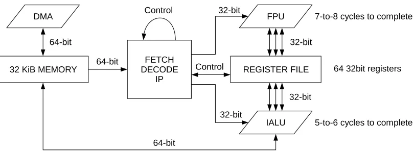
3.2.3 The Epiphany eCore
The Epiphany processing cores (eCores) are custom dual-issue RISC processors with a 64-word register file. Each eCore features an integer arithmetic logic unit (IALU) for basic integer and memory operations and a floating-point unit (FPU). FPU and IALU instructions can be issued simultaneously each clock-cycle, as long as the instructions don't both use the same registers. Control instructions, such as branching and register data movements cannot be issued in parallel with IALU or FPU instructions. Instructions are executed in-order in a pipelined fashion, but can finish out of order. Whenever an instruction executes, the target operand registers are locked until completion. If another
Figure 6: E16G301 Coordinate system conventions and example routes for node (0,2) and (2,0) up and down traffic
0 1 2 3
0
1
2
3
E
A
S
T
e
Li
nk
(2,0)
RELEVANT BACKGROUND 3.2 Epiphany Architecture
It is important to note that the IALU only supports data load/store, shift operations, addition, subtraction and bitwise operations. Integer multiplication and division, as well as floating-point division, are emulated in software. These emulated operations are retrieved from external memory when called, and introduce both a large memory and processing overhead. These operations should be avoided. Each eCore is accompanied by a DMA engine featuring two independent channels, capable of transferring 64 bits every clock cycle. More detailed information on the DMA engines and the eCore instruction set can be found in [1].
3.2.4 Maximizing Epiphany Performance
The specified peak performance for the Parallella board is listed in Table 1. These peak performance numbers are only valid under specific conditions, which are discussed in this section. One important thing to note is that although technically the E16G301 supports clock rates up to 1GHz, it runs at only 600MHz on the Parallella board.
Specification Value
Zync Frequency 667MHz
E16G301 Frequency 600MHz
E16G301 Peak Floating Point Performance 19.2 GFLOPS
Peak Bandwith Zync – E16G301 600 MB/s up, 600MB/s down
DDR3 Memory 1GiB
[image:20.595.97.502.106.254.2]Power Consumption E16G301 [email protected], 600MHz [14]
Table 1: Adapteva E16G301 / Parallella peak performance specification summary Figure 7: simplified eCore hardware overview, showing dual-issue capability
FPU
FETCH DECODE
IP REGISTER FILE
IALU 32 KiB MEMORY
64-bit 64-bit
32-bit
32-bit
32-bit 32-bit
DMA
64-bit
Control
7-to-8 cycles to complete
RELEVANT BACKGROUND 3.2 Epiphany Architecture
Maximizing Memory Performance
The local memory of a node in the E16G301 is split into four banks of 8KiB. The local memory banks are 64 bits wide and can be accessed once every clock cycle for 8 to 64bit transfers. This means maximum performance for local memory is obtained when 64 bits are read or written every clock cycle [1]. For 600MHz this would equal 4.8GB/s for each bank simultaneously.
The DMA engine, instruction fetch stage and IALU can access separate memory banks simultaneously, so for optimal performance, different memory banks should be used for the program instructions and input and output data.
Accessing off-chip memory is typically very slow and should be avoided whenever possible.
Maximizing Network Performance
The network is optimized for on-chip writes over the cMesh. This allows an 8-to-64bit transaction every clock-cycle. Maximum performance is achieved for 64bit transactions every clock-cycle, leading up to 4.8GB/s per link at 600MHz.
For the E16G301 specifically, an errata item in the datasheet states that the DMA engine can only issue a transfer every other clock cycle, limiting the maximum performance to 2.4GB/s per link at 600MHz. A 1.5 clock-cycle latency is introduced for every router that is passed in the network, so routes should be kept short if latency is important. How the 1.5 cycle can occur is not elaborated. Each eLink can send and receive 8 bits per clock-cycle simultaneously, and every eLink transfer requires a 40-bit header per data payload of 32-64 bits. For 64bit transfers with increasing address order only (0x0..0x4..0x8 etc..) the eLink can enter a burst mode, omitting the packet header until the sequence is broken. At 600MHz this results in 600MB/s per eLink in each direction simultaneously. For non-burst and read transfers, only 1/4th of this bandwidth can be achieved ([14]).
Maximizing eCore Performance
The maximum eCore performance is achieved by using fused multiply-add (FMADD) instructions. These instructions will first multiply two arguments and accumulate the result with a third. They can be issued every clock cycle, and are counted as two floating-point operations, resulting in the specified 1.2 GFLOPS/eCore at 600MHz.
RELEVANT BACKGROUND 3.2 Epiphany Architecture
3.2.5 Initial E16G301 Performance Estimates
Now that the requirements of the application domain and the specifics of the Epiphany architecture have been introduced, an initial peak performance estimate of the beam-former and channel filters on the Epiphany architecture can be made. For this we start with the following assumptions:
1. The ADC input stream consists of 16-bit fixed-point samples.
2. The output type of any stage is a complex number. A single precision (2x 32bit) floating point representation will be used since that is most efficient on the Epiphany architecture.
3. Every component can be used at it's peak performance at 600MHz
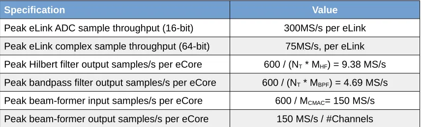
4. A MAC can be performed by one fused-multiply add/subtract instruction every clock cycle Based on these assumptions, the cost equations for the tasks (p.16) and the peak performance numbers of the Epiphany architecture, we can determine the peak throughput per task, as is shown in Table 2. These are the absolute maximum rates we can expect for the eLink and eCore at 600MHz, and they scale linearly with the system clock-rate.
Specification Value
[image:22.595.86.514.348.477.2]Peak eLink ADC sample throughput (16-bit) 300MS/s per eLink Peak eLink complex sample throughput (64-bit) 75MS/s, per eLink Peak Hilbert filter output samples/s per eCore 600 / (NT * MHF) = 9.38 MS/s Peak bandpass filter output samples/s per eCore 600 / (NT * MBPF) = 4.69 MS/s Peak beam-former input samples/s per eCore 600 / MCMAC= 150 MS/s Peak beam-former output samples/s per eCore 150 MS/s / #Channels
Table 2: Epiphany architecture peak throughput per front-end receiver task
RELEVANT BACKGROUND 3.3 CRISP / Recore Xentium RFD Summary
3.3 CRISP / RECORE XENTIUM RFD SUMMARY
The closest available platform in terms of architecture to which we can compare the Epiphany architecture is the Recore Xentium RFD. This is a many-core processor developed and used during the CRISP project ([2]) to determine the feasibility of a fault-tolerant and scalable front-end processing system ([15],[4]). An overview of the Recore Xentium RFD is given in Figure 8:
The Recore Xentium RFD features nine Xentium processor nodes [XE0..XE8], a dependability manager (DM) and two memory nodes (MEM). The processor nodes are based around a VLIW architecture, with a data-path that can execute four 16-bit MACs/cycle. Five Recore Xentium RFD processors are combined to form a single CRISP platform with a combined processing power of 180 16-bit MACs per clock cycle ([4]), or 36 GMACS at 200MHz.
Recore Xentium RFD Network-On-Chip
The Recore Xentium RFD on-chip network uses a 2D mesh topology, with one additional link as shown in Figure 8. It is a packet-switched network with wormhole type flow-control, and allows for 4 virtual channels ([16], chapter 1.4) per physical network link.
Instead of XY routing, adaptive source routing is used, where routes are not fixed, but determined at run-time in supporting hardware and software. Routers can be configured to assign different weights to each virtual channel in order to asymmetrically distribute the available bandwidth over the active connections.
[image:23.595.61.526.194.385.2]Off-chip data communication is done through six independent off-chip connections that function as transparent links to and from the NoC. There is a difference in clock frequency between the on- and off-chip networks (50MHz off-chip vs. 200MHz on-chip) resulting in one quarter of the bandwidth per off-chip link compared to the on-chip links (800Mbit/s vs 3200Mbit/s at 200MHz).
Figure 8: Recore Xentium RFD architecture overview (Taken from [15])
Memory tile (64KB)
4
3
0
1
2
5
S
M
R
X
E6X
E7X
E8X
E5X
E4X
E3X
E0X
E1X
E2MEM MEM
DM
XENTIUMR DSP
tile
Router
MCP
link (offchip)
RFD
registers
Dependability
Manager
IP
–
NOCinterface
NOC
link
RELEVANT BACKGROUND 3.3 CRISP / Recore Xentium RFD Summary
3.3.1 Front-End Receiver Mapping and Performance
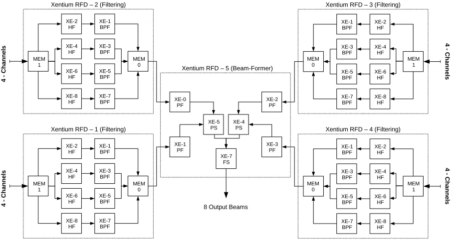
During the CRISP project, a front-end receiver with 16 input channels, using 32-tap filters with a Hilbert filter decimation factor of 8 and 8 output beams was implemented on the CRISP platform ([17]). The mapping used for this implementation is shown in Figure 9:
In Figure 9, the filtering is performed by four out of the five Recore Xentium RFD processors. Each RFD processes four input channels. Beam-forming is done in several stages on the fifth Xentium RFD. First, the four output channels of a single filtering Xentium RFD are multiplied with the suitable coefficients in the partial beam-forming task (PF). The resulting channels are summed in the partial summing (PS) and final summing (FS) tasks.
All processing is done using a 16-bit data representation of each real valued sample, and two 16-bit values for complex valued samples. This allows the efficient use of the parallel data-paths of the Recore Xentium RFD, but also requires proper scaling of the coefficients and input samples to avoid overflow and loss of precision.
[image:24.595.73.534.193.437.2]The final implementation can sustain an input sample rate of 25MS/s per channel. To achieve this, the filters and beam-former have been optimized and implemented in the assembly language. In order to determine the bottleneck and slack-time in this implementation, several performance measurements where performed, of which the results are repeated in Table 3.
Figure 9: Front-end receiver mapping on CRISP processing platform featuring five Recore Xentium RFDs
(NC=16, DHF=8, DBPF=1, NT=32, FS = 22MS/s @ 200MHz)
XE-2 HF XE-4 HF XE-6 HF XE-8 HF XE-1 BPF XE-3 BPF XE-5 BPF XE-7 BPF MEM
1 MEM 0
Xentium RFD – 2 (Filtering) Xentium RFD – 3 (Filtering)
XE-1 BPF XE-3 BPF XE-5 BPF XE-7 BPF XE-2 HF XE-4 HF XE-6 HF XE-8 HF MEM
0 MEM 1
XE-2 HF XE-4 HF XE-6 HF XE-8 HF XE-1 BPF XE-3 BPF XE-5 BPF XE-7 BPF MEM
1 MEM 0
Xentium RFD – 1 (Filtering) Xentium RFD – 4 (Filtering)
XE-1 BPF XE-3 BPF XE-5 BPF XE-7 BPF XE-2 HF XE-4 HF XE-6 HF XE-8 HF MEM
0 MEM 1
Xentium RFD – 5 (Beam-Former)
XE-0 PF XE-1 PF XE-2 PF XE-3 PF XE-5
PS XE-4 PS
XE-7 FS
8 Output Beams
RELEVANT BACKGROUND 3.3 CRISP / Recore Xentium RFD Summary
Task to Process SamplesInput SamplesOutput ProcessingTime Idle Time (waitingon data)
Filtering
Hilbert Filter (HF) 1024 128 12 μs 29 μs
Bandpass Filter (BPF) 128 128 14 μs 26 μs
Beam-Forming
Partial Beam-Forming (PF) 256 512 10 μs 12 μs
Partial Summing (PS) 512 512 2.5 μs 20 μs
Final Summing (FS) 512 512 2.5 μs 20 μs
Table 3: Recore Xentium RFD performance details for front-end receiver implementation
Table 3 shows that a lot of processor time is spent waiting on input data to arrive. Also, it is interesting to note that the bandpass filter takes only marginally longer to process than the Hilbert filter, even though at least twice as many calculations need to be performed for this filter task. This suggests that the implementation of the bandpass filter is more efficient than that of the Hilbert filter task.
Based on the initial peak-performance estimates for the E16G301 in Table 2 (p.22), the processing times of the filters for the same data lengths can be determined. These are given here in Table 4:
Task to Process SamplesInput SamplesOutput Processing TimeRecore Xentium Expected E16G301Processing Time
Hilbert Filter 1024 128 12 μs 13.7 μs
Bandpass Filter 128 128 14 μs 27.3 μs
Table 4: E16G301 and Recore Xentium RFD initial performance comparison (estimated)
Table 4 shows that in the best-case, a single eCore at 600MHz cannot keep up with a single Xentium processor tile at 200MHz. This is mainly due to the large amount of parallel execution units on the Xentium processors, allowing up to four MACs per clock cycle. A single eCore can only perform a single MAC per clock cycle.
4 Benchmarking & Related Work
Thus-far, we have presented the peak performance numbers for the Epiphany architecture given in Table 1 and Table 2, which are derived from the Epiphany architecture specifications. However, it is unclear what percentage of this peak performance can realistically be achieved. In this chapter the expected peak performance for real-world applications is investigated by looking at related work. Based on the results, several missing benchmarks are identified. The missing benchmarks are implemented and the results are presented in chapter 5.
4.1 RELATED WORK
During this research, five other research papers discussing the performance of the Epiphany architecture have been published. In [18], a very detailed description of the development of a high performance matrix multiplication application on the Epiphany architecture is given. The authors of [19] and [20] compare the Epiphany architecture to a custom many-core processor and an Intel-I7 processor, and in [21] and [7], the use of a standardized Message-Passing-Interface (MPI) on the Epiphany architecture is investigated. The most relevant results in these research projects are repeated here for convenience.
4.1.1 eCore performance
The performance achieved for the application built in [18] are shown in Table 5. Here large matrix multiplication problems are split into smaller pieces over multiple eCores. The results include on-chip communication, but not the time required to get the operands from off-chip memory. A very strong dependence of performance on the problem size is observed. For small matrix sizes a large software and communication overhead limits the performance to only 26% of peak. In the best case 85% of peak performance is achieved.
Matrix Size (per-eCore)
Number of eCores used and total GFLOPS achieved
2x2 4x4 8x8
GFLOPS %-Peak GFLOPS %-Peak GFLOPS %-Peak
8x8 1.25 26.1 5.07 26.4 20.30 26.4
16x16 3.12 65.1 12.76 66.5 51.41 66.9
20x20 3.58 74.7 14.36 74.8 57.62 75.0
24x24 3.84 80.1 15.43 80.4 62.17 81.0
[image:27.595.82.511.555.704.2]32x32 4.06 84.7 16.27 84.7 65.32 85.1
BENCHMARKING & RELATED WORK 4.1 Related Work
When the total matrix size is increased such that the operands no long fit in local memory, additional communication over the eLink is required. Table 6 shows the results for a few of these cases. Here it become very clear that even through the local eCore problem sizes allow high computation efficiency, the bottleneck for these applications is the communication over the eLink interface.
Matrix Size (per eCore, total)
Total
GFLOPS % of Peak
%-Time spent on
computation %-Time spent oncommunication
32x32 per eCore
512x512 total 8.32 10.8 12.8 87.2
32x32 per eCore
1024x1024 total 8.52 11.1 13.1 86.9
24x24 per eCore
1536x1536 total 6.34 8.2 10.9 89.1
Table 6: Epiphany G4 matrix-multiplication peak performance when using shared memory ([18])
The results in Table 5 and Table 6 were obtained for a highly optimized assembly implementation on the Epiphany G4 processor. The authors note that implementation was time consuming, but achieving maximum performance with the GCC compiler proved difficult. However, in [7], the authors present four applications implemented in the C language for the E16G301 with the use of a special FMADD C function that reaches similar performance levels. The peak performance for each application in [7] is summarized in Table 7.
Application GFLOPS % of Peak on computation%-Time spent %-Time spent on
communication
(32x32 per eCore, 128x128
total) Matrix-Multiplication 12.02 62.6 63 37
N-Body Particle Interaction 8.28 43.1 99 1
Heat-Stencil 6.25 32.6 45 55
2D-FFT Transform 2.5 13.0 60 40
Table 7: E16G301 peak performance and computation/communication ratio achieved in [7] for four different applications
BENCHMARKING & RELATED WORK 4.1 Related Work
4.1.2 eMesh Performance
The E16G301 used by [7] and the G4 used by [18] both suffer from a problem with a FIFO buffer in the network interface of the mesh-nodes. According to the data-sheets this only affects the maximum outgoing bandwidth of a mesh-node. Unfortunately, it is unclear how much the performance is affected by this. Also a problem with the DMA engines on the E16G301 only allows a data transfer every other clock cycle, effectively halving the maximum achievable bandwidth.
Despite these errata, a peak DMA performance of 1963.6MB/s (82% of 2.4GB/s for 32bit transfers) is obtained in [18]. In [21] a peak transfer rate of 1262MB/s is achieved for 64bit direct-writes. Finally, in [7], a peak rate of 1000MB/s is achieved. The results of [21] and [18] are shown in Figure 10. Here a start-up behaviour is observed. This is likely caused by the DMA start-up time and direct-write software overhead. Interestingly, the direct transfer rates achieved in [21] are much higher than the results shown for direct writes in [18].
The data sizes presented in both graphs in Figure 10 are somewhat ambiguous. In [18], it is unclear what the message size actually denotes, since 48KiB does not fit in local memory. It is assumed that this is the total data transferred by all 64 nodes, as their test routes packets through all mesh-nodes. In this case the 49152 byte transfer results would be for 768 byte transfers per node.
In [21], data is transferred in 512-byte blocks, and only total data sent changes by sending multiple packets sequentially. It is noted that the measurement was done for the transfer of all sub-matrices per node. For a 32x32 matrix multiplication, both matrix operands would be divided into sixteen 8x8 sub-matrices, resulting in two 8x8 matrices per node. Each elements takes up 4 bytes, resulting in a total transferred size of 512 bytes per node for this case.
Both representations in Figure 10 are relatively hard to translate to a new application, where the interest would mainly be in the time it takes to transfer a certain amount of data from node to node. A clearer representation is given in [7], however much lower bandwidths are achieved.
Neither [18] or [21] achieve peak-performance, nor use 64bit DMA transfers required to meet this peak performance. The effect of sharing links on this performance, or how the DMA performance is affected
Figure 10: Left: cMesh Bandwidth - DMA vs Direct Write (as presented in [18])
Right: Direct-Write MPI bandwidth using 512-byte transfers (as presented in [21])
32x32 48x48 64x64 80x80 96x96 112x112 128x128 0
200 400 600 800 1000 1200 1400 1600
506 772
1102 1169
1258 1243 1262 Direct Write
Matrix Size (Single-Precision Elements)
B
a
n
d
w
id
th
(
M
B
/s
)
4096
BENCHMARKING & RELATED WORK 4.1 Related Work
4.1.3 eLink Performance
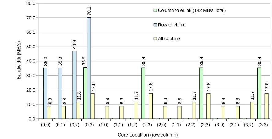
Table 8 shows the achieved bandwidth per node in [18], when four nodes send 2KiB packets over the same eLink simultaneously during two seconds. The total bandwidth achieved is 150MB/s, one quarter of the maximum achievable bandwidth of 600MB/s. This is expected, as burst transfers for 32bit writes are not possible. The results show that the bandwidth is not equally divided, in fact, the authors claim that for the G4 starvation can occur when even more nodes share an eLink.
Source Node Sent Packets eLink Share (%) Bandwidth (MB/s)
[0,0] 61307 41.8 62.8
[0,1] 48829 33.3 50.0
[1,0] 24414 16.6 25.0
[1,1] 12207 8.3 12.5
Table 8: eLink bandwidth per node when four nodes send 2KiB packets during a two second period (as presented in [18])
The total bandwidth achieved in Table 8 is 150MB/s for 32bit transfers, suggesting that sharing an eLink does not influence the eLink performance. However, when multiple nodes attempt to perform 64bit burst transfers over the same eLink, it is likely that the eLink will alternate communication slots between nodes. This would effectively break the burst-mode capability of the eLink, limiting the peak bandwidth to 150MB/s instead of 600MB/s. This would have a large impact on application design, as only one node should be allowed to communicate over an eLink at any given time.
4.1.4 Epiphany Power Consumption
Currently there is very little information available on the actual power consumption of the Epiphany architecture. The only power consumption numbers available are those from the E16G301 datasheet [14]. Figure 11 shows a more convenient representation of the values in [14]. Also the peak efficiency is shown for these results, assuming peak performance was achieved for the values in [14].
100 200 300 400 500 600 700 800 900 1000 1100 0.00
5.00 10.00 15.00 20.00 25.00 30.00 35.00
0.00 0.20 0.40 0.60 0.80 1.00 1.20 1.40 1.60 1.80
Power (W) GFLOPS / Watt
Frequency (MHz)
G
F
L
O
P
S
/
W
a
tt P
o
w
e
r (
W
)
0.86 Volt 0.75 Volt
0.69 Volt
0.95 Volt 1.01 Volt
BENCHMARKING & RELATED WORK 4.1 Related Work
Figure 11 shows that 32 GFLOPS/watt can only be achieved at 400MHz. At 1GHz, this reduces to roughly 21GFLOPS/watt. This result differs from the performance of 32GFLOPS/watt at 1GHz shown in the STARS multi-core survey ([9], Table 12 p.73). The details of the power measurements in [14] (Achieved GFLOPS, network load, part contributed by the separate components) are not given. This means no information is available on the actual achieved performance per watt for a real-world test-case. Also, the effect of core voltage on the power consumption is not known at this point.
4.1.5 Remaining Work
So far we have seen that the achievable performance on the eCore depends heavily on the application. In order to determine a realistic measure of peak performance of our application, the front-end receiver tasks should be implemented and analysed.
For both the eMesh and eLink, the related work has shown some interesting behaviour and performance numbers, however, it is unclear what causes the observed DMA start-up behaviour, and also the performance for 64bit DMA transfers over the eMesh and eLink is still unknown. To investigate this and other topics further, several custom micro benchmarks will be developed. The design of these benchmarks is discussed in the next section, which will cover the following topics:
1. Message Size vs. Bandwidth: Here the effect of total transfer size on the achieved bandwidth
on both the eMesh and eLink, using DMA and direct-write transfers is measured. The goal is to find the cause of the start-up behaviours observed in Figure 10, and to determine the best method to use for each message size to use for our application.
2. eLink Bandwidth Sharing: The peak off-chip bandwidth is only maintainable using
burst-mode transfer. We expect sharing the eLink will break the burst burst-mode transfer, however this is not documented or tested in related work.
3. eMesh Bandwidth Sharing: The links in the cMesh should support 4.8GB/s, however the
results so far show that this bandwidth is not easily achieved. It is interesting to investigate how the eMesh handles sharing of network bandwidth, as this determines for a large part the freedom of placement of tasks on the Epiphany platform.
BENCHMARKING & RELATED WORK 4.2 Custom Micro-Benchmarks
4.2 CUSTOM MICRO-BENCHMARKS
In this section, several custom micro-benchmarks are introduced to give some insight in the open topics presented previously. In addition, a simple benchmark program provided by Adapteva ([22]) is run to test the Parallella board network bandwidths. The results of the benchmarks presented here are given in chapter 5.
4.2.1 Message Size vs. Bandwidth
The effect of the total transfer size on the effective bandwidth of the DMA engine is tested using one sending mesh-node. This node will send increasing packet sizes up to 8KiB using 64bit DMA transfers. The time it takes to configure the DMA engine is measured, as well as the total time to perform the transfer. This is done for both configurations shown in Figure 12.
4.2.2 eLink Bandwidth Sharing
Measuring the effect of sharing an eLink during maximum performance operation will be addressed by introducing the three different configurations shown in Figure 13. All active nodes will send a continuous stream of 8KiB packets using 64bit DMA transfers. The time required to send each packet is measured.
First, the four nodes closest to the eLink send data simultaneously. Here it is expected that the bandwidth will be shared equally amongst all nodes, but drops significantly. Second, four nodes with varying distance to the eLink, will send data. This should introduce similar starvation as shown in Table 8, but shown for 64bit transfers. Finally all sixteen nodes will send data simultaneously. This allows comparing the bandwidth achieved with one, four and sixteen nodes to see if significant routing
Figure 12: DMA transfer size micro-benchmark test-cases. Left: Data is sent over eMesh
Right: Data is sent over eLink to shared memory
RECV SEND SEND
EAST eLink
2
3
0
1
2
3
0
1
A.
2
BENCHMARKING & RELATED WORK 4.2 Custom Micro-Benchmarks
4.2.3 eMesh Bandwidth Sharing
Here we introduce two cases in Figure 14. First, four nodes in a cross will send a continuous stream of 8KiB packets towards a single node. The achieved bandwidth per node is measured. Here we expect that the total bandwidth is limited by the receiver memory, and that the remaining bandwidth is shared equally among the senders.
In the second case in Figure 14, crossing traffic is introduced. One node continuously sends data to a receiving node from East to West on the cMesh. This traffic is then crossed by one to four other transfers from North to South. The effect on the achieved bandwidth from East to West is measured.
Figure 13: eLink micro-benchmark test-cases. A: Four nodes closest to the eLink send packets. B: Four nodes
with varying distance to the eLink send packets. C: All nodes send packets.
SEND 8KiB SEND 8KiB SEND 8KiB SEND 8KiB SEND 8KiB SEND 8KiB SEND 8KiB SEND 8KiB SEND 8KiB SEND 8KiB SEND 8KiB SEND 8KiB SEND 8KiB SEND 8KiB SEND 8KiB SEND 8KiB SEND 8KiB SEND 8KiB SEND 8KiB SEND 8KiB SEND 8KiB SEND 8KiB SEND 8KiB SEND 8KiB 2 3 0 1 2 3 0 1 2 3 0 1 2 3 0 1
EAST eLink
2 3
0 1
C. B.
A.
Figure 14: eMesh sharing configurations. Left: four nodes in a cross send to a receiver. Right: Four
sets of nodes send from North to South, effect on performance from East to West is measured
SEND
RECV
SEND
A SEND B SEND C
BENCHMARKING & RELATED WORK 4.2 Custom Micro-Benchmarks
4.2.4 E16G301 Power Consumption
The power supply of the E16G301 is split into a core power and IO power section. Both need to be measured to determine the total power. Unfortunately the IO power rail is shared with many other devices on the Parallella board, and cannot be easily decoupled. For useful measurements a method is required that allows separation of the E16G301 power and that of the other devices. Also, the measurements need to be properly synchronized with the software to be sure that the power measurements don't include possible idle times of the E16G301.
The E16G301 runs at 1 Volt on the Parallella. The datasheet shows that for 600MHz, the E16G301 can go down to as low as 0.86 Volt. This has a very large impact on the power consumption. For a fair minimum power consumption measurement, ideally we would like to vary the E16G301 core voltage to see the effect of this on the power consumption.
The issues with the power measurements are addressed by building a small measurement circuit that reports measured power over an on-board I2C bus. The I2C bus can also be used to configure the core voltage regulator for the E16G301, allowing us to set the E16G301 core voltage from software. The details of this measurement circuit are given in Appendix C: Power measurement setup.
Several test cases will be measured, each at multiple E16G301 core voltages:
• eCores: eCore power consumption will be measured by measuring core-power consumption
during execution of a heavy load micro-benchmark. No data is transferred during this benchmark keeping the eLinks and eMesh networks idle during this measurement.
• eMesh: The eMesh power consumption will be measured increasing the distance of a transfer
between nodes, without changing the number of active nodes or the amount of data sent. The increase in power consumption over distance is contributed by the increased network activity.
• eLink: the eLinks are powered by the IO power-rail shared with multiple devices. To measure
the eLink power consumption, we let a single node repeatedly send and stop sending data over the East eLink. The measured variation in the power consumption on the IO power-rail should reflect the active power consumption of the eLink. Also, the eLinks can be switched off by hardware, by repeatedly switching the North/South/West eLink on and off simultaneously, we can determine the standby power of the eLinks.
5 Micro-Benchmark Results
In this chapter we present the results for the micro-benchmarks on the E16G301. We start by looking at a small benchmark application provided by Adapteva [22]. This benchmark copies 8KiB from multiple sources to several destinations, and measures the time it takes for this transfer to complete. The results for the E16G301 and the Parallella board are shown in Table 9.
From To Type Time (us) / 8Kb Bandwidth (MB/s) % of Peak
ARM eCore Read 1255.3 6.5 4.4
ARM eCore Write 586.9 14.0 2.3
ARM DRAM Copy 42.3 193.8 ?
eCore DRAM Read 89.2 91.8 61.2
eCore DRAM Write 32.4 252.5 42.1
eCore eCore Read 20.0 409.0 68.2
eCore eCore Write 6.1 1342.2 28.0
Table 9: Parallella communication performance measured by Adapteva benchmark application (average of 50 measurements)
On the parallella board, there are two ways to get data onto the E16G301 from shared memory. This is either through a write transaction from the host processors, or through a read transaction from the mesh-nodes. Table 9 shows that the fastest method to get data onto the E16G301 on the Parallella board is through a read transaction initiated by a mesh-node, which achieves 91.8 MB/s. This is much lower than the maximum achievable bandwidth of 600MB/s at 600MHz, and also lower than the limited 150MB/s that should be possible for eLink read transactions.
It is not entirely clear what causes this, but a read transaction has to travel over the eLink twice, first as a read transaction of 9 bytes, and then as a write transfer of 9 to 13 bytes (depending on the transfer size) from the host returning the data. The time it takes to process the read-request on the host-side will influence the achieved bandwidth.
The direct transfers from the ARM processors to the E16G301 are very slow (14.0 MB/s), possibly due to the use of the memcpy() function by the provided host library which can cause a lot of overhead on the eLink transfers, or due to the overhead introduced of reading from memory first, and then writing the result over the same AXI bus to the FPGA eLink hardware. These low host-to-mesh-node transfer speeds are only applicable for the Parallella board and not for the Epiphany architecture in general, demonstrated by the much higher rates when the eCores transfer data over the same eLink.
![Figure 1: Phased-array antenna receive chain processing overview [9]](https://thumb-us.123doks.com/thumbv2/123dok_us/9848994.486072/13.595.75.486.368.574/figure-phased-array-antenna-receive-chain-processing-overview.webp)
![Figure 8: Recore Xentium RFD architecture overview (Taken from [15])](https://thumb-us.123doks.com/thumbv2/123dok_us/9848994.486072/23.595.61.526.194.385/figure-recore-xentium-rfd-architecture-overview-taken.webp)
![Table 5: Epiphany G4 matrix-multiplication peak performance when using on-chip memory ([18])](https://thumb-us.123doks.com/thumbv2/123dok_us/9848994.486072/27.595.82.511.555.704/table-epiphany-matrix-multiplication-peak-performance-using-memory.webp)