University of Warwick institutional repository:http://go.warwick.ac.uk/wrap
A Thesis Submitted for the Degree of PhD at the University of Warwick
http://go.warwick.ac.uk/wrap/59155
This thesis is made available online and is protected by original copyright. Please scroll down to view the document itself.
Super-precision programmable
current source
for coil/magnet actuators
by
David C. Dyer
BSc(Hons) CPhys MinstP CEng MIEE MBCS
Submitted for the award of PhD
at
The University of Warwick
Department of Engineering
Dedicated to
My wife
for her kindness, patience and encouragement My children
who have missed me for several years My parents
for the education that underpins all that follows
Exhortation
Awake! - brave scholar and resume the fight, Work all day and then most of each night. With rigour and method decide what's right, And then with luck, you'll see a great light
Acknowledgement
Summary
This thesis describes the design and development of a super-precision programmable current source that can deliver up to about
±
100 rnA to an inductive load. The load is intended typically to be a coil in a coil/magnet actuator that provides a force which is proportional to the current, and results in a linear and well defined movement of an elastic flexure mechanism. The particularly demanding application of long-range x-ray interferometry required two tracking current sources that offered a resolution to better than 1 part in 500,000 and this could not be satisfied by commercially available instruments. Consequently it was necessary to design, construct and test two identical supplies (or drives); a non-trivial and very demanding task since exceptionally slow drives scans needed to be accommodated. Temporal stability is therefore critical. Although the operational bandwidth can be kept small, noise up to over 1 kHz must be rigorously suppressed to avoid exciting resonances in the system being driven. Commercial 20-bit digital-to-analogue converters could not be utilised to provide a resolution of 1 part per million, because they are invariably designed for audio applications and have unacceptable drifts with temperature and time. The integral non-linearity had to be less than ±O.0007% (15 ppm) and the design actually achieves ±O.5 ppm by using an embedded precision analogue-to-digital converter to form a servo-loop within each drive. A desk-top computer (PC) accepts setpoints via a serial communications channel, and simultaneously controls the servo-loops for two drives by the exchange of simple messages via optically isolated links. The major components within each drive are, an embedded 8-bit micro-controller, two DAC's providing coarse and fine voltage settings, a precision voltage-to-current converter, a precision ADC and an ADC which monitors critical nodes, all of which are discussed in considerable detail together with the algorithms and software in the PC and microcontroller. Circuit simulations were an important part of preliminary studies and are presented along with measures of actual performance. It is shown that the drives achieve not only a resolution of 1 ppm but that all other operational parameters are of a similar order. A number of proposals are made for alternative methods which represent the foundations for future work.-Contents
Summary
1 Application of precision coil/magnet actuators 1
1.1 Coil/magnet geometries and actuators 1
1.2 X-ray interferometry 3
1.3 Coil arrangements for translation and twist 6
1.4 Requirements for a programmable current source 7 1.5 (Un)suitability of commercial programmable current sources 10
2 Design ideas, problems and constraints 12
2.1 Generic problems in high-precision electronic instrumentation 12
2.1.1 Drift with temperature 13
2.1.2 Drift with time 15
2.1.3 Noise 15
2.1.4 Interference in mixed digital/analogue circuits 16 2.2 Applicability of published designs for programmable current sources 17
2.2.1 Review of - Programmable current supply for inductive load
(1986) 18
2.2.2 Review of - Microcomputer-controlled, programmable current source for NMR measurements at very low temperature (1991) 18 2.2.3 Review of - Development of a programmable current source
(1993) 19
2.3 Design ideas for a suitable 1 ppm DAC 20
2.3.1 Pulse width modulation (1: 106) 21
2.3.2 Multiple level pulse-width-modulated DAC (1:64) 22
2.3.3 Coarse and fine DACs 24
2.4 Minimising risk in the NPUDTI project 25
2.4.1 Coil self-heating effects and cures 26
2.4.2 Embedded versus sub-system controllers 27
2.5 Proposed design 28
3 Drive circuits in detail 31
3.1 Power supplies 31
3.2 Microcomputer 33
3.4 Coil drive circuit 35
3.5 Heater/Drive 2 circuit 38
3.6 Auxiliary devices 39
3.6.1 Power supply for chopper-stabilised amplifiers 39 3.6.2 Clock generator for chopper-stabilised amplifiers 39
3.6.3 Monitor ADC and temperature sensors 40
3.6.4 Isolated serial link 41
3.6.5 Non-volatile memory 42
3.6.6 Configuration switches 42
3.7 Component layout and Printed Circuit Board 43
4 Embedded Software 48
4.1 Initialisation 49
4.2 Serial interface and command structure 50
4.3 Timer interrupt and service routines 51
4.4 Command decoder and command execution 52
4.5 Floating-point interpreter 57
5 Slave PC Software 60
5.1 Main program 60
5.2 Screen presentations 62
5.3 Calibration 65
5.4 Communication ports and interrupt driven buffers 70
5.5 Closed-loop control strategy 71
5.6 Keyboard operation 72
5.7 Messages from and to host computer 72
5.8 Utility functions and procedures 73
6 Performance Measures 74
6.1 Noise sources and predicted performance 75
6.1.1 Noise in voltage reference and DAC's 75
6.1.2 Response of Voltage-to-Current converter 76
6.1.3 Precision current sensing resistor RSI 80
6.2 Measured responses 81
6.2.1 Precision ADC 81
6.2.2 Power-on/off transients 84
6.2.3 Step response 85
6.2.4 Noise in the coil 86
-6.2.5 Closed-loop response 6.3 X-Ray interferometer fringes
90 92 7 Alternative approaches and new proposals
7.1 Availability of improved components 7.1.1 Voltage references at 1 ppm/tC 7.1.2 Delta-Sigma ADCs
7.1.3 Linear operational amplifiers with low drift 7.1.4 Buffer amplifiers
7.2 Use of an external voltmeter
7.3 Application of switch capacitor building blocks 7.3.1 For voltage halving and inversion
7.3.2 In voltage-to-current conversion
7.3.3 Deglitching and demultiplexing a DAC 7.3.4 Interpolation in a time demultiplexed DAC
7.4 PWM DACs and Field Programmable Gate Arrays (FPGA) 7.5 Suppression of power onloff transients
7.6 Proposal for dual drive
96 96 96 97 98 99 99 101 101 102 106 108 109
110 111
8 Final comments and conclusion 8.1 Settling time of DACs 8.2 Additional auxiliary circuits 8.3 Commercial considerations 8.4 Conclusion
115 115 116 118
120
References 121
Annex 1 : Circuit diagrams Annex 2 : PCB layout
Annex 3 : Embedded software Annex 4 : Slave PC software Annex 5 : PSPICE simulations
127 137 138 177
211
Appendix A : AD 1175K ADC Appendix B : Precision resistor
List of Figures
Figure 1.1 - Flexure mechanism with coil/magnet actuator
Figure 1.2 - Silicon monolith [1. 14]
Figure 1.3 - Silicon monolith with two magnets [1.18]
Figure 1.4 - Coil Arrangements
Figure 1.5 - Jumping fringes
Figure 1.6 - Commercial current sources [1.20 to 1.23]
Figure 2.1 - Commercial DACs
Figure 2.2 - Pulse-width-modulated DAC
Figure 2.3 - Multiple-level PWM N-Bit DAC
Figure 2.4 - Piecewise linear DAC
Figure 2.5 - Proposed heating jacket
Figure 2.6 - General arrangement of equipment
Figure 2.7 - Block diagram of drive
Figure 3.1 - Connections to Precision ADC Module
Figure 3.2 - DAC(s) and summing amplifier
Figure 3.3 - Circuit for voltage-to-current converter
Figure 3.4 - Clock timing for chopper-stabilised amplifiers
Figure 3.5 - Top-view of assembled PCB
Figure 3.6 - Oblique-view of chassis and PCB
Figure 3.7 - Appearance of completed system
Figure 4.1 - Port allocation
Figure 4.2 - Command address table
Figure 4.3 - Preparing primary DAC
Figure 4.4 - Interpreter operations
Figure 4.5 - Example of using interpreter
Figure 5.1 - Main program listing
Figure 5.2 - Screen when Source
=
HOST PCFigure 5.3 - Screen when entering CALIBRATION
Figure 5.4 - Typical recorded calibration data
Figure 5.5 - Coding for calibrate-cycle
Figure 5.6 - Combined DACs during calibration
Figure 5.7 - Assignment of communication channels
Figure 6.1 - Component noise
Figure 6.2 - Voltage-to-Current converter simulated by PSPICE
Figure 6.3 - vtoil Transient response
2
5
5
6
9 10
20
21
23
25
27
28
29
34
36
37
40
45
46
47
50
53
54
58
59
61
63
66
67
68
69 70
75
76
77
-Figure 6.4 - vtoil Frequency response
Figure 6.5 - vtoi2 Frequency response
Figure 6.6 - Noise of OPA654
Figure 6.7 - Precision ADC readings
Figure 6.8 - Precision ADC readings and filtered values
Figure 6.9 - Low frequency noise of filtered ADC readings
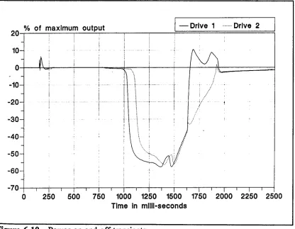
Figure 6.10 - Power on and off transients
Figure 6.11 - Step response
Figure 6.12 - High gain test amplifier
Figure 6.13 - Noise spectra of coil-current
Figure 6.14 - MATLAB script files for spectral analysis
Figure 6.15 - Frequency response of test amplifier
Figure 6.16 - Error in ramped output
Figure 6.17 - NPL Monolith - 2.1 fringes/mVor 0.67nm/mV - G3
78
79
80
82
83
83
84
85
87
88
89
90
91
93
Figure 6.18 - NPL Monolith - 2.1 fringes/mY or 0.67nm/mV - G4 94
Figure 6.19 - Warwick (stiff) Monolith - 0.067 fringes/mY or 2Opm/mV - G5 94
Figure 6.20 - Warwick (stiff) Monolith - 0.067 fringes/mY or 2Opm/mV - G6 95
Figure 7.1 - OPA177E and OPA627BM specifications 98
FigureJ.Z - Use of external voltmeter
Figure 7.3 - Voltage halving and inversion
Figure 7.4 - Differential to single-ended conversion
Figure 7.5 - Switched capacitor V-to-I with bias
Figure 7.6 - Response of switched capacitor V-to-I
Figure 7.7 - Response of switched capacitor V-to-I
Figure 7.8 - Deglitched and demultiplexing a DAC
Figure 7.9 - Demultiplexed DAC waveforms
Figure 7.10 - Better demultiplexing
Figure 7.11 - Interpolation in a time demultiplexed DAC
Figure 7.12 - Using a lO-bit PWM DAC as the coarse DAC
Figure 7.13 - Power on/off protection
Figure 7.14 - Proposal for dual drive
Figure 8.1 - Circuit depicting DACs with different time constants
Figure 8.2 - Responses when DACs have different time constants
Figure 8.3 - Embedded diagnostic amplifier
Figure 8.4 - Alternative communication schemes
100
101
102
103
104
105
106
107
108
109
ADC
BCD
cps
DAC
dc
DNL DTI
EEPROM
FSO
IEEE
1NL
LSB
MSB
NPL
NS
PCB
ppm
PTB
PWM
PZT
RAM
RP
rms
THD
Abbreviations
Analogue to digital converter
Binary coded decimal
counts per second
Digital to analogue converter
Direct current
Differential non-linearity
Department of trade and industry
Electrically erasable programmable read only memory
Full scale output
Institution of Electrical and Electronic engineers
Integral nonlinearity
Least significant bit
Most significant bit
National physical laboratory
National semiconductor corporation
Printed circuit board
parts per million
Physikalisch- Technische Bundesanstalt
Pulse width modulation
Piezo-electric transducer
Random access memory
Radio frequency
Root mean square
Total harmonic distortion
-Chapter 1 Application of precision coil/magnet actuators
"Thefirst experimental investigation of the interaction between coils carrying electric currents was performed by Ampere during the years 1820-5, and the work was continued by Oersted, Biot and Savart. ... Both a magnet and a current-carrying coil
are said to produce a magnetic field described by a
flux
density B, which exertsforces on other coils or magnets", [l.lJ
It seems unlikely that these scientists could have foreseen the far reaching consequences of the discoveries which underpin the present work. Itwould probably have been beyond their belief that it is now possible to control current flow so finely that, through the subsequent minute variations in forces between coils and magnets, movements smaller than the atomic spacing of silicon can be made and measured. But such is now the case and the remainder of this thesis is devoted to an explanation of a technique which does just this, and in particular the design, construction and testing of a super-precision programmable current source. Such sources can have many applications but the current work arose from the need for a technology breakthrough to control adequately low-speed nanometric movements using electromagnetic actuators and the thesis addresses issues in this context.
1.1 Coil/magnet geometries and actuators
In regard to the relationship between forces due to current carrying conductors the simplest 'mathematical object' to be analyzed was the force between two infinitely long parallel conductors. Of course this arrangement cannot be realised an practice and further analysis was performed on closed loops, ideal coils and solenoids in order to determine the variation of magnetic field strength, H, with position. Probably the most notable early achievement was by Helmholtz (1821-1894) who showed that if two identical circular coils of radius
a,
are placed parallel and co-axial a distancer
apart, the field near their geometric centre is uniform over a significant region when
r=a. This is because at the centre dH/dr, d2H/dr2 and d3H/dr3 are all zero. (actually
Helmholtz made a more notable contribution to science in 1847 when he put forward the 'Law of conservation of energy'. But it was rejected for publication by the editor of Annalen der Physik! [1.2])
may involve integrals which have no analytic solution. Alternatively expressions may be so complicated that it is difficult to plot graphs of H(x,y ,z) by hand. However with the advent of digital computers numerical modelling became easier and new expressions were developed.[1.3]
Ifa bar magnet is positioned near or within a coil, it experiences a force which is proportional to the current in the coil. If it is fixed to an elastic support, it will move until the force due to the current (driving force) equals the elastic restoring force. A simple arrangement is depicted in Figure 1.1.
Figure 1.1 -Flexure mechanism with coil/magnet actuator
Even if the restoring force varies linearly with displacement, the net movement is usually not linear because the driving force varies with absolute position. However work done by Smith and Chetwynd [1.4] shows there to be a optimised design of coil such that the driving force is essentially independent of position over a certain region. The significance of this is not in the design of large coils with constant fields over millimetres, but rather small coils which provide a useful range of several micrometres. Such coil/magnet combination can then be used in a wide range of applications under the general heading ofnanotechnology. For example, in the design of high precision translation mechanisms [1.5] and the control of instruments for the measurement of surface profile [1.6]. Of course coil/magnet combinations have been used for moving-coil motors; e.g. in loudspeakers, and for the head positioning in some disc drives; as well as force balancing techniques for weighing [1.7]. In trying to scale moving-coil devices to provide small movements the problems associated with mechanical coupling become increasingly severe. Consequently moving-coil systems are considered as macroscopic applications and not discussed again. Instead the
Base
-emphasis is on systems using moving-magnets to achieve microscopic displacements. In moving to ever smaller currents, forces and therefore displacements, it becomes increasingly difficult to measure the actual displacement and thereby characterise the behaviour of precision actuators. Itshould be noted that there is a difference between the detection of small movements and the measurement of absolute position. For example capacitive gauges [1.8] can detect picometre movements and, by a servo-loop, maintain the relative position of two components, but are not so useful for long range absolute measurements. Optical laser interferometers can be used to measure displacements down to about 10 nm relatively easily [1.9], but this is still large compared with the potential resolution afforded by magnet/coil actuators which may better 10 pm [1.10]. Consequently an alternative method of measurement is needed which is reliable, accurate and above all traceable to the international definition of the metre.
1.2 X-ray interferometry
To provide a traceable measurement an internationally recognised scale is needed, and this may be provided by the lattice parameter for silicon, which has been referenced to the absolute length scale at PTB in Germany [1.11] and is characterised to a precision of better than 1part in 107•In 1965 Bonse and Hart [1.12] showed how an
X-ray interferometer could be built, and subsequently Hart suggested that itbeused to create an 'Angstrom ruler' [1.13]. However, according to Chetwynd [1.14] it was not until 1983 that the application as a ruler was seriously pursued with the demonstration of its use as a microdisplacement calibrator by Chetwynd et al [1.15]. The operation of an x-ray interferometer is theoretically complex (see cited references) and is not directly of concern to the work here. Suffice it to say that scanning one thin 'blade' of a single crystal of silicon past other parallel blades causes a modulation in the intensity of a transmitted x-ray beam that varies sinusoidally with the pitch of the lattice. In effect, the system behaves as an incremental grating of pitch equal to the lattice parameter.
that small unwanted movements of the coil caused by vibrations in the ground, do not result in such vibrations in the magnet attached to the monolith, because the force in almost independent of position [1.4].
Bowen, Chetwynd and Smith were all established members of the Centre for Microengineering and Metrology (renamed in 1994 as the Centre for Nanotechnology and Microengineering) at the University of Warwick, when the Department of Trade and Industry (DTI) invited tenders for the design and manufacture of a "Traceable secondary standard displacement facility with sub-nanometre resolution - DTI reference MPU 8/0.13". Their collective experience lead to a proposal for an instrument which used a silicon monolithic x-ray interferometer, which in principle could meet the required resolution of 0.02 nm over a range of 10p.m. That is to say the mechanical properties of a suitable monolith were sufficiently well understood that together with a coil/magnet actuator the required movements could be obtained if the current in the coil could be controlled sufficiently well. In fact two programmable current sources were needed because, in order to obtain fringes over the desired range, there must be active compensation for twisting caused by a variety of secondary and parasitic effects which may be ignored over shorter ranges. At this time the author became involved with the project and defended the view that the design of a programmable current source with a resolution of 1 part in 500,000 was feasible, although a non-trivial and potentially very difficult task. The intended mode of operation of the instrument meant that not only was the resolution to approach 1 part per million (ppm), but also the noise, integral non-linearity and stability over long periods needed to be of the same order.
Figure 1.2 shows the general construction of a silicon monolith for use as an x-ray interferometer, while Figure 1.3 gives the arrangement of the drive proposed to the DTI. It has a cross bar and two magnets and coils in order to provide a trim torque to compensate for parasitic motion. Also, the use of two coils results in a lower total power dissipation for a given force.
Although much of the discussion for the requirements of a precision programmable Current source which follow refer to x-ray interferometry, it would be wrong to conclude that this it the only application. Many other applications come to mind including atomic force microscopy, x and y translation for surface measurements, magnetic lensing in electron microscopes and movement of mirrors in optical metrology. The requirements for long-range x-ray interferometry are particularly demanding and are regarded as a sensible vehicle for developments and discussions.
-collimated
Scintillation ccunter+-i (counter on forward diffracted beam not sho1f11)
Figure 1.2 - Silicon monolith [1.14]
moving
leaf type flexures
[image:15.542.66.486.51.737.2]permanent magnet
1.3 Coil arrangements for translation and twist
For a given monolith there may be an axis along which a force can be applied that will result in translation without any rotation. However imperfections in the machining of the leaf-springs and the inability to define the exact position of the magnet make it such that a torque, and therefore rotation or twist, is expected. For long-range interferometers the problems associated with unwanted rotation cannot be ignored as they degrade the contrast of the fringes and active compensation schemes must be used to ensure optimum performance.
[image:16.542.94.439.291.594.2]In order to provide independent control over linear force (for translation) as well as torque (for twist compensation), at least two current sources are needed, and Figure 1.4 shows three topologically different, yet symmetrical, coil arrangements which provide this.
~---~
a)
1
HI
L',JJ
b)
1
H2
LT2
===========_j
Figure 1.4 - Coil Arrangements
The arrangement shown in Figure l.4a) is the most obvious extension from previous work. It shows a main linear drive, L, associated with the centre coil and magnet MO, and a torque drive, T, with the outer two magnets MI and M2. The outer coils are wound in opposite directions so they can induce a torque with no net linear force. Unfortunately, magnets M1 and M2 will not be identical, nor for that matter will be the geometry of the coils or the distances from the main axis of the platform, and this will result in a linear displacement whenever a simple torque is required.
-A refinement is shown in Figure l.4b) which uses only two magnets with over-wound coils. Once again the intention is to be able to trim any twist of the platform by careful control of a torque. There are numerous sources of error which can result in either an undesirable torque or linear force. However the arrangement is better than a) because the force required for linear movement of the platform is now split between two coils. This means that the current in each coil need be only half that using one coil, and the power per coil will be reduced to one quarter. In turn this means the effects of local heating are reduced.
In both a) and b) the current for the linear drive, L, will be orders of magnitude greater than the torque drive, T. This difference is easy to accommodate by using similar drive circuits acting on coils with a differing number of turns.
The arrangement in Figure l.4c) is easier to build and understand than b) but necessitates two drive circuits with exactly the same performance if both coils are to produce the same forces for the same control codes. In fact this is the ideal situation and differences between MI and M2, as well asymmetries in the geometry of the coils will require the offsets and gains of the two drives to be different, but maintained at a fixed ratio. The names of the drive signals are changed from L and T, to LTI and LT2, to reflect the change in use; suitable increases in common to them both will cause a linear movement, while differential changes will cause a rotation.
Two coils may be used to achieve control of translation and twist in one plane but it may be advantageous for some mechanisms to allow controlled movements in several planes. The application of forces at a number of positions may cause direct and desirable movement, or may compensate for unwanted parasitic effects. The designs for flexure mechanisms, possibly using multiple webbed hinges, are beyond the present work, but it is possible that design rules may be reconsidered if programmable current sources are sufficiently cheap and accurate, that numerous coil/magnet actuators may be employed.
1.4 Requirements for a programmable current source
if a source may be used for the interferometer it will necessarily be capable of numerous other applications, although perhaps limited by economic considerations. To satisfy the requirements of the DTI project the resolution must be at least 1 part in 500,000, and it is practical to try and better this by aiming for 1 part in 106, or 1
ppm. It is reasonable to assume that, whatever means is used to determine the current, it will rely on digital components, which form a binary scale. This binary scale needs 20 bits since 1 ppm most closely maps to 1 bit in 220, (where
220
=
1048576). Furthermore, given a range of 10ILm and that the<
111>
lattice parameter for silicon is about 0.313 nm, there will be (10 x 10-6)/(0.313 x 10-9)=
31949 fringes.
Itis now important to mention that during operation of the x-ray interferometer as a calibration facility, other position sensors will measure the displacement of the monolith and, to test their accuracy in different absolute positions, it is convenient to move several micrometres in a single 'jump'. Without this facility it is necessary to track the movement across every (intermediate) fringe, and to do so requires photon counting to take place at two points in each fringe. The x-ray energy is kept low to avoid unwanted heating; consequently the count rates are low, and it takes many
(> 10) seconds to determine the position within a fringe. For example, a 1 ILm
movement corresponds with about 3000 fringes, which implies a scan takes 30000 seconds (say), or over 8 hours. Jumping over fringes relies on being confident that the actuator, and indirectly the current source, has indeed placed the monolith to within half a fringe width of the expected fringe. So long as the correct fringe has been found, the exact position
±
10 pm may be found by making small additional movements and monitoring of changes in photon count rates. Alternatively full determination of the position within a fringe may be obtained without further movement if a phase-stepping technique is incorporated [1.19]. Ifa binary scale is perfectly matched to the position of the fringes, then N binary counts will correspondtoexactly N fringes. Unfortunately, whatever digital-to-analogue conversion process is used will be inaccurate and even if it offers monotonic performance and resolution to 1 ppm a lower bound can be calculated for its integral non-linearity if 'jumping' is to be achieved. The permissable uncertainty can be explained with the aid of Figure 1.5. Consider a jump from fringe x to fringe x+n, and that, in the first instance, the position is bounded by points p and q (± 112 fringe). A small increase moves these bounds to p' and q', but the interpretation about absolute position is ambiguous because a fringe boundary has been crossed. Suppose, instead, that the position is bounded by the points a and b (± ~fringe). Then a small increase bounds
-the position by a' and b' which is within -the same fringe and allows determination of the absolute position by interpolation. In fact the constraint of
+
lA fringe is unnecessarily tight, but on a binary scale it is the next best range when + 1/2 fringe is rejected.Ideal
jump
Fringe
x
x+n!
a
b
- --- --- .._..--·,1--- _.._-_ __ _ -- ..--- --- ---
----,
r
, ,
Figure 1.5 - Jumping fringes
Since the range of 10 JLmcontains 31949 fringes, which maps closely to a 15-bit scale with 32768 intervals, the corresponding required integral non-linearity (INL) is ± lA of the least significant bit (LSB). Expressed as a percentage of full scale this is ±0.OOO7%, and if it were not for the need for 20-bit resolution a practical realisation of this bound can be achieved using a 16-bit DAC with an 1NL of +1/2 LSB, such as part DAC729KH by Burr Brown.
Based on previous work with coil/magnet actuators within the Centre for Nanotechnology and Microengineering, an upper bound of
±
100 mA was placed on the current requirements for a single coil. Two identical sources were needed for this application and a thorough survey revealed that no commercial supplies had the necessary performance.I.S (Un)suitability of commercial programmable current sources
There are many manufacturers that make programmable voltage and current sources which are designed to deliver power to a load and not intended as reference sources for calibration. In studying the catalogues for companies such as Hewlett Packard, Fluke and Philips, a pattern emerges as to the general characteristics of the supplies. Firstly, there are very many more supplies with voltage outputs than with current outputs, and the maximum output power may be between 50 and 2000 watts. Secondly, the resolution is often stated in such a way as to suggest the use of aN-bit DAC, where N is typically 12 to 14. Figure 1.6 shows the 'best' of what was available in 1992, and only Marconi model 103A comes close to the required performance. Even though it offers a resolution of about 1 ppm the linearity is quoted at only 0.005% (50 ppm) on the
+
100mA range.Make Hodel Range Step Res. Ten.,.Co linearity Noise Connents
bits
re
Keithley 224 :l:100mA SO~ 12 12~ 1 100ppm Non-Inductive load
Fluke PM2831 :l:IA 12 1 1 2mA
HP 6625A SOOmA 100~ 14 1 1 O.lmA
Marconi 103A :l:llOmA 100nA 20 1 0.005" t DC Reference
?= parameter not available
Figure 1.6 - Commercial current sources [1.20 to 1.23]
Although every effort was madeto identify all commercial sources at the start of this research work, model 103A by Marconi was not found until after the design ideas based on pulse width modulation discussed in this thesis had already been established independently. Itis therefore interesting to note that an entry in a Marconi catalogue [1.20] describes the instrument as " .. a dc voltage and current reference source .. based on a unique pulse width modulation digital/analogue conversion principle .. ". The resolution is quoted as 100 nA from
±
100 nA to±
109.9999 mA, which supports the view that internally 6 decades of binary coded decimal (BCD) counters are used to create a digital controlled PWM signal. Detailed study of the specifications shows the linearity for the voltage output to be 0.001 %, which is 5-times better than the current output. Perhaps a voltage-to-current converter is employed with inherent non-linearities that limits the performance. Unfortunately no specification is provided for current noise, and with limited linearity the instrument would not have been good enough for the intended application.
Chapter 2 Design ideas, problems and constraints
The suitability of driving flexure mechanisms by high-compliance coil/magnet force actuators to provide smooth precision movements was discussed in section 1.1. The resolution may be as good as ±5 pm over 10 ",m if the drive current(s) can be controlled sufficiently well, but this is difficult because it represents a range to resolution of 2,000,000: 1. Since a typical operating voltage is 2 volts the uncertainty must be less than 1 ",V, and at this level electronic noise becomes the limiting factor. Operating the coil at constant voltage was acceptable for the original experiments but since the force depends on current it is much better to operate the coil at constant current, and thereby eliminate changes due to fluctuations in the coil resistance which occur as the temperature changes.
As a design goal, and because of the constraints of a particular application in X-ray interferometry, it was necessary to design a programmable current source with a resolution of 1 part in 1 million (or 1 part in 220), with correspondingly small drift, noise and non-linearities. This specification is extremely challenging as problems rapidly escalate in trying to go beyond about 17 bits. This chapter discusses these problems and culminates in the proposal for a specific approach and design.
2.1 Generic problems inhigh-precision electronic instrumentation
To many people the design of electronic circuits is considered as something of an Art [2.1], perhaps because the union of components to make a meaningful whole is seen in much the same way as an artist blending colours and textures to create a pleasing effect. Even in more informed circles this notion is given some credence as the inventiveness needed to design an elegant circuit for a specific function is not commonplace, and the designer is perceived to have a talent akin to that of an artist. However the analogy is deficient and misleading for the electronic design engineer will invariable use models of the real components during the design process, whereas the artist will use real components (pigments) almost straight away. If the object of electronic design is to produce a circuit diagram that has aesthetic appeal then perhaps it is an art form, but unlike a painting the circuit diagram is merely an intermediate stage. What the designer really seeks to create is a physical working circuit, which can only operate as expected if there is a strong correspondence between the meaning attributed to the symbols on the circuit diagram and the behaviour of physical components. Unfortunately the models of analogue circuits become increasingly
-simplistic and inaccurate as the desired resolution increases, and very much more effort and understanding is needed to predict the overall performance of each circuit element.
For super-precision current sources where the resolution and linearity are to be about 1 part per million of full scale output (ppm FSO) there is the implied requirement that long term drift, noise and variations with temperature be correspondingly small. This necessitates models of components to hold true for six orders of magnitude, which is often not the case. Models are developed either by theoretical analysis of the physical principles by which a component works, by experimental observations, or more usually by studying data sheets published by a manufacturer. For an individual component it may be possible to characterise its operation to better than 1 ppm under all anticipated operating conditions in the near future, but this does not cater for hitherto undiscovered mechanisms of aging due to, say, background cosmic radiation. Itis most unlikely that information such as this is in a data sheet, but that may not be sufficient reason to ignore the possibility.
Very often a circuit diagram shows a line that represents zero volts, and is generally considered as an ideal conductor with no voltage drops along it. Of course at high frequencies this 'ideal' conductor has a significant inductive component which designers of Radio Frequency (RF) circuits are taught to model. At low frequencies and down to direct current (de) the resistive component of a track on a printed circuit board is very often ignored. Voltage drops of several millivolts are commonplace, and must be considered in precision instruments where a potential difference of even 101'V may be undesirable. This kind of effect is often static and may be compensated, but it does show an obvious source of difficulty when designing precision circuits. Four areas which cause dynamic problems are of sufficient importance that they are now mentioned individually. The intention is to highlight specific difficulties so they may be considered appropriately during the description of various designs in later pages.
2.1.1 Drift with temperature
reveals that the drift figure is obtained by dividing the change in voltage output by the change in temperature, when the temperature changes from O°C to 70°C. The drift is the mean rate of change and may be much higher at a particular temperature if the response is non linear, see [2.2]. On the other hand, manufacturers quote the maximum drift that may be expected of, say, 10 ppm/oC with the implication that most components will be significantly less. Is a Gaussian distribution assumed with
30' limits at 0 and 10 ppm/r'C, or is some other distribution assumed? What percentage of components will have a drift of less than 4 ppm/oC ? These are typical and reasonable questions that are not readily answered, but affect greatly the expected performance or a particular instrument built from such components.
Specifications for the drift of input or output voltage with temperature are available for most components, and these often show the effect to be positive or negative. The distribution is usually Normal with a mean of zero and the limits given are derived from
±
3 standard deviations. A naive approach is to characterise the worst case drift of an instrument by adding together all of the worst case drifts given in the data sheets for each of the components in use. This approach is flawed becausea) It assumes the contribution to overall drift from each component is additive with the same weighting, and in general this will not be so. The very least that should be done for a particular circuit is to consider a weighted sum.
b) The changes with temperature may be non-linear so that for a particular temperature the drift may be much better/worse that expected. For example, in the Schlumberger digital voltmeter type 7081 an extensive number of components are used to compensate for the 'curved' voltage drift of the reference diode [2.3].
c) There are sources of drift with temperature other than active components. Passive components also have temperature coefficients and in critical sections of the circuits these must be considered. However what is often forgotten are thermoelectric potentials caused by junctions of dissimilar metals, and these may be several /LV/oC [2.4]. Some precision amplifiers have drifts which are several orders of magnitude lower than thermoelectric effects so the latter will dominate.
d) Self-heating may cause unexpected local temperature gradients and changes in ambient temperature may not be of such importance.
-It is clear that drifts caused by temperature changes need to be considered most carefully.
2.1.2 Drift with time
Drift with time, when the temperature is held constant, is another type of drift that is often ignored because it is so small. This may well be true for many applications but for precision measuring/controlling instruments long term drift may be a significant concern. Manufacturers do not provide such specifications except for components which have to respond to d.c. conditions. For example chopper-stabilised amplifiers, precision voltage references, and high resolution ADCs and DACs. Chopper-stabilised amplifiers, by their very design, have extremely low drifts with time; typically less than 0.01 ppm/month. For the others, drifts of about 10 ppm/1000 hours are often quoted, and since slow 'runs' of 10 hours are possible a change of 0.1 ppm may not be insignificant. Also over a period of several months the drift may be more significant than that caused by changes in operating temperature.
2.1.3 Noise
The effect of random fluctuations of current in electronic components have been studied extensively and characterised [2.5]. Many physical processes are present in real semiconductor devices which result in noise with frequency components that vary throughout the spectrum. For a circuit with many components, noise at its output may usually be considered as a combination of incoherent voltage (or current) sources. In data sheets values for noise in particular frequency bands may be given, but for a specific band it is usual to compute the noise based on the graphs provided showing the noise power spectral density in p.V/.JHz versus frequency. Idealised models of components [2.6] often assume that flicker (lit) noise is dominant below some critical frequency fe' while above that white noise is present. This leads to equations which may not model a real device. For example the low frequency noise spectrum of bipolar operational amplifiers may be close to lIf but for amplifiers with JFET inputs
Noise is also presented in data sheets in terms of a peak-to-peak (Pk-pk) value which is usually in JJ.V over some frequency band. Such figures may be combined in a weighted sum to provide an estimate for the maximum pk-pk value for a compound circuit, but this is not the same as the rms value. If the peaks are short-lived they may have a significant amplitude but negligible energy, and care is needed in the prediction of the overall effect(s).
2.1.4 Interference in mixed digital/analogue circuits
The functionality of many instruments can be increased by the inclusion of a local or embedded microprocessor, which may be programmed to perform a wide range of useful operations. All microprocessors require additional memory and input/output devices to operate, and due to the high speed of execution a complex digital waveform is generated on all interconnecting buses. The waveforms have high frequency components of the order of Megahertz, but may also have low frequency components of the order of 10-100 Hz, because of the cyclic nature of many control programs. When precision analogue components share the same power supply, or even just a common ground line, these frequency components are seen as unwanted disturbances on the analogue output. The method of coupling is not usually by electromagnetic interference but rather by changes in the potential of the shared wire(s) due to transient currents caused by changes in digital outputs. With the advent of optical-couplers, which allow the exchange of digital information without direct connection of electrical circuits, isolated sub-systems can be formed. Only the minimum of data is passed across the coupler(s) to control the analogue circuits, and interference is kept to a minimum. Unfortunately, in the case of an analogue subsystem which uses multiple digital-to-analogue circuits it is necessary either to use numerous couplers in parallel, or to employ digital circuits to decode a serial data stream passed via one coupler. The former choice is expensive while the latter becomes self-defeating as digital logic is needed in the supposedly analogue-only circuit.
An alternative approach now exists because complete low-power microcontrollers are available where the microprocessor, memory and input/output ports are all integrated into one device. Consequently all interconnections are kept 'on-chip' and signals on the output ports may be connected directly to analogue subsystems without causing undue interference. There is still the possibility of unwanted coupling but separate power supplies for digital and analogue subsystem joined at only one star point and
-with suitable decoupling capacitors minimises the effect of digital transients. Itis also
necessary to arrange for digital control signals to be routed on the printed circuit
board (PCB) so that they are kept clear of analogue components.
For reasons of safety all mains-operated instruments in metal chassis should have the
metalwork connected to the earth of the supply. Many instruments also connect the
zero volt rail to the chassis and therefore to the local earth. But if a microcontroller
has a serial port for communication with a remote computer which itself is joined to
a local earth it is possible to create an earth loop with one connection via a cable
between the two ports and another via the mains earth wiring. Unfortunately mains
earth points around a building are not always at the same potential and unwanted
interference is generated within 'ground' loops. It is not essential to have the zero
volt rail(s) of the instrument joined to its chassis, and this removes the ground loop,
however this may lead to undesirable potentials between 0 volts and the chassis.
Isolation may also be provided using opto-couplers, and in particular with an optically
coupled serial link which is now available in integrated form.
2.2 Applicability of published designs for programmable current sources
About a 12 papers from the last 10 years were found using the BIDS [2.7] computer
database services, but not all were appropriate because of differences in interpretation
of the term 'programmable'. Four different categories of current sources were
identified which were programmable
a) at the time of manufacture
b) by selection of suitable resistors or switches
c) by digital codes but for high voltages
>
200 Vd) by digital codes and for use in instrumentation
Only 3 papers were found in category d) and each of these is discussed in more detail
to gain insight into what has been achieved, and to highlight good and bad features.
This style of presentation and comparison is a little unusual but appropriate because
of the lack of published work in this area. All three papers have the common feature
that the DACs used do not have sufficient resolution and there is no real likelihood
2.2.1 Review of - Programmable current supply for inductive load (1986) [2.8] The circuit diagram is difficult to follow because all the elements shown as operational amplifiers have unrecognised (Russian) part codes. However it is clear that the voltage output of a 12-bit digital-to-analogue converter feeds a power amplifier using discrete transistors, which achieves voltage-to-current conversion with current gain. A 2-terminal reference resistor driven by an ungrounded inductive load provides voltage feedback. The DAC is controlled by digital latches which are connected directly to the data bus of an Elektronika NTs-80-20/1 microcomputer. The age and tone of the paper suggest this to be a desk-top computer with a microprocessor and auxiliary components rather than a single-chip device. The text also states "The preamplifier has a Goldberg circuit; the high-frequency circuit is regulated by a low-frequency modem channel. This ensures an output current instability of
s
0.1 mA over the temperature range 20-50°C" The exact meaning of these words is unclear but it is apparent from the circuit that there are both ac and dc signal paths around the power amplifier.There ,are four aspects of the design which limit its application as a high precision current source.
a) The digital logic is not isolated from the analogue components and there may be ground 'loops' and/or other interference effects.
b) The DAC is only 12 bits giving a resolution of 1 part in 4096 c) There is no analysis about noise contribution of the components
d) End effects at the 2-terminal reference resistor will be significant at higher precision.
2.2.2 Review of - Microcomputer-controlled, programmable current source for NMR measurements at very low temperature (1991) [2.9]
This paper describes a circuit which is intended to offer 16-bit resolution. Serious attention is given to the problems encountered in the design of precision electronic instruments. A complete circuit is not presented but the general description is of a microprocessor-based (Z80) instrument with an IEEE-488 interface, and an analogue sub-system that is optically isolated. The needs for low-noise operational amplifiers and a reference resistor with a low thermal coefficient of resistance are mentioned, as is the problem with glitches from the DAC. The usefulness of monitoring the state
-of the power amplifier is also explained and provision is made for appropriate components. There are graphs which show the change in current divided by the mean current taken over several hours to be less than 5 x 10⁻⁵•This corresponds to about
1part in 214, which is large considering a 16 bit DAC is used. There are two areas of weakness which limit the resolution and accuracy of the design.
a) The DAC is stated to be a l6-bit DAC703JP by Burr-Brown; however inspection of the data sheet shows the 'J' part to guarantee monotonicity to only 13 bits. Also there is no guarantee on the maximum temperature coefficient for the internal voltage reference, although
±
10 ppm/oC is given as typical. Selection of the 'C' grade part would have offered monotonicity to 15 bits and a maximum temperature coefficient of+
15 ppm/oC.b) The text states ".. The reference resistor RN made from manganin has a nominal value of 0.2 0 .. ", and the circuit diagram shows a 2 terminal device. There will be end effects caused by the connection of copper wires or printed circuit board traces to the manganin and a 4 terminal resistor is preferable, where the current sensing connections are not the same as the current forcing connections.
2.3 Design ideas for a suitable 1 ppm DAC
Beginning with the assumption that the current source to be designed would contain a DAC to generate a reference voltage followed by a near perfect voltage-to-current converter, it was thought appropriate to investigate further commercial DACs. There are many semiconductor manufacturers who supply digital-to-analogue converters but after a thorough study of the parts available none was considered able to meet the design target, which requires resolution and monotonicity to 20-bits. Figure 2.1 shows the best of the parts that were studied together with important operational parameters and general comments.
Device Res. Mono. Comnents
Texas Instruments, Motorola, National Semiconductor, Plessey - No suitable OACs
DAC-HP16B 16 14
AD1145BG 16 16
AD1139J 18 18
AD1860 18 15
DAC1138K 18 NA
DAC72~KH 18 16
PCM63P 20 16/17
Gain Power Manufacturer
±ppm mW
rC
15 675 Datel
0.1 2.5 Analog Devices
4 825 Analog Devices
25 110 Analog Devices
0.8 900 Analog Devices
5 1200 Burr Brown
25 225 Burr Brown
Figure 2.1 - Commercial DACs
Resolution too low Lowest power and drift
'Best' DAC found PCM Audio DAC
Requires external reference to
achieve quoted drift.
Monotonic to 16 bits, but high power
PCM Audio DAC
Burr Brown describes its PCM63P device as a 20-bit monolithic Audio DAC, but careful inspection of the text reveals a statement which says ".. the extremely low Total Harmonic Distortion (THD) performance is typically indicative of 16-bit to 17-bit integral linearity,... the relationship between THD and linearity, however, is not such that an absolute linearity specification for every individual output code can be guaranteed". These comments are typical ofDACs designed for use in Compact Disc audio systems where THD is more important than absolute linearity, and therefore such DACs should be avoided. Itis also worth noting that the PCM63P has a full-scale current output of 2.00 rnA, which means that a precision current (rather than voltage) amplifier is needed in order to maintain accuracy whilst providing a nominal
100 rnA of coil current.
Although the ADl139J offers monotonic performance to 18 bits it is obviously not capable of 20-bit performance and is therefore not sufficiently 'accurate', where 'accurate' is used to mean that
-resolution and non-linearity are
<
1 ppmtemperature coefficient is
<
1 ppm/oClong-temp drift is below 1 ppm / 100 hours, (say)
What was required is an almost ideal 20-bit DAC, and no commercial source can
supply it. Instead a special system must be built. Three different techniques were
considered which might achieve this and these are discussed in tum.
2.3.1 Pulse width modulation (1: 106)
It is well known that digitally controlled pulse-width-modulated signals may, in
principle, be filtered to produce analogue signals whose level can be increased
linearly with respect to digital control signals. An arrangement for a 20-bit converter
is shown in Figure 2.2 where the digital demand is continually compared with the
output of a 20-bit counter. When a is greater than bthe a> boutput becomes a logic
1 and causes the analogue switch to connect the resistor to a reference voltage rather
than ground. When REF
=
219 a square wave is produced with a 1:1 mark to spaceratio, and a mean value of Vrel2 appears after the filter along with unfiltered ripple.
20-Blt REF Precision
SwItch Low Pess Filter
R
10 MHz. clock
lI)b vs tIme
voltege
large II small a
[image:31.542.120.466.411.680.2]time
With present technologies there are two practical limits to this approach. Firstly the time for the comparison to be performed, and secondly the response time of the analogue switch. Ifthe counter is clocked at 10 MHz, the comparator has only 100 ns to perform its function, and in the worst case, a delay of less than 5 ns per bit is needed. Unfortunately even at 10 MHz. the cycle time is about 0.1 s and requires low-pass filters with long time constants to extract the d.c. component of the waveform. Active filters may reduce the settling time but they introduce their own drifts. Digital circuits may operate at more than 100 MHz and the period T may be reduced, but there is still the requirement for an analogue switch with sufficiently fast response times, and this is not available. Even at 10 MHz, when REF= 1 only one pulse of lOOns duration results and the analogue switch must respond within a negligible time of say5ns. Charge injection from the digital control line to the filter is also a major limitation. Consequently the technique was considered infeasible.
2.3.2 Multiple level pulse-width-modulated DAC (1:64)
In the previous approach the clock rate is limited by delays in the comparator and temporal characteristics of the analogue switch. It is advantageous to reduce the number of bits in the comparator, so that the cycle time may be decreased without increasing any frequency components. This may be achieved by splitting the range, and Figure 2.3a shows the arrangement when two references are used, together with a three-way analogue switch. The most significant bit (msb) of the latched input is used to decide which reference voltage is used, while the
a>
b output still determineswhen it is used. When msb =0, Vre/2 and Ov are used, and when msb = 1, V refand
Vre/2 are used. Saving only one bit in the comparator is not very significant but the idea may be extended in principle to use 2n reference levels. Unfortunately an analogue switch with 2n+ 1 inputs is not very practical when n is greater than about four. However the same effect will be achieved by using an ideal N-bit DAC and modulating its output between levels n and n+ 1, as shown in Figure 2.3b. With more analogue levels the number of time zones for pulse-width-modulation may be reduced and a higher repetition frequency obtained. The higher the frequency the more easily the signal may be filtered to remove ripple in the 0 to 1000 Hz band to which many precision mechanism can respond.
The idea of modulating the output of a DAC is intuitively correct but requires formal analysis. Consider a converter with a 20-bit overall performance where N-bits are devoted to a normal DAC and bits to the control of its output. In particular the
-Precision Swltch<es)
Low Pass Filter R
Vref
-+0-'
Vref
2 ---+-0
0v
20-BIt REF
0V~C
a>b
a)
Most Significant
Bit
10 MHz. clock
R N-blt DAC
0V~C
Code osc1l1ates
[image:33.542.81.488.52.358.2]between levels n and n+1
b)
Figure 2.3 - Multiple-level PWM N-Bit DAC
bits determine the ratio of time the DAC spends at its n and n + 1 levels.
Let any 20-bit code be n:m where O~n~(2N-l) and O~m~(2M-l) and suppose
Vdac=f(n) =.E..xvre.f
2N
then average output
=
vout is given byv
=
f(n). (2M-m)+f(n+l) .mout 2M
then when
m=O
=
Vre.f[n+l __ 1_]2N 2N+M
There are conflicting requirements for the values of N and M. On the one hand a small value for M is desirable because this would allow a high repetition rate for the
pulse-level-and-width-modulated signal, which could then be filtered more quickly.
However, becauseN
+
M=20, a small value for M implies that a high precision N-bit DAC is needed, which is precisely what is not available. With current technology a sensible compromise is achieved when M =6 and N = 14. By switching between levels n and n+
1 in the ratio 0:64 to 64:0 and filtering the output, a piece-wise linear interpolation is obtained. The settling time for the DAC limits the maximum frequency but in principle the output may be filtered much more readily and have a settling time which is only 10 s of milli-seconds. Unfortunately the output of most DACs have a characteristic 'glitch' when switching between levels, which is worst for a majority change. For a 14-bit DAC this occurs at code levels of 8191 to 8192, but still occurs at all other levels to a greater or lesser extent. Consequently the output of the filter will not be an interpolation between levels. Even in the absence of 'glitches' the net output may not have the desired integral non-linearity which is limited by the linearity of the 14-bit DAC. Figure 2.4a shows a typical response of a 14-bit DAC where, for the sake of explanation, the non-linearity appears greatly exaggerated, while Figure 2.4b shows the interpolation between levels around zero, but is representative of the response throughout the range. Ifthe interpolation is exact there is a piece-wise linear fit between adjacent DAC levels, which' themselves have a deviation from a straight line. Stated another way, it is clear that the local gains vary and that the integral non-linearity over the entire range is determined by the 14-bit converter and is therefore no better than ih least significant bit, or 1 part in 215•The values of Nand M may bechanged but the nature of the response will remain the same. Once again the technique was considered infeasible. (In fact it is infeasible in its basic form, although it may form the basis of a more subtle approach, see
chapter 7.)
2.3.3 Coarse and fine DACs
A well known measurement technique is to use coarse and fine scales. The same principle may be applied to two DAC in order to create a DAC with greater resolution. However it is naive to believe that two 8-bit DACs may be used to create a single 16-bit DAC simply by summing the two DACs with relative weightings of 1 and 1/256, The difficulty lies in the fact that the output levels of the coarse DAC are
not evenly spaced and the fine DAC needs to have a different gain factor associated with it for every pair of adjacent levels from the coarse DAC. In this way the
-"'3Vref 8192
Non-linear
but ./
monotoolc ./
./
piece-wise llneer and monotoolc
./ ./ ./ Ideal
./ response
--7 Incre8S1ng
Olgltlll
Code
--7 Increasing
Dlgttlll
Code
./ ./ ./ ./ ./ ./ ./ ./
./ -3Vref
8192
-Vref
[image:35.542.73.497.48.301.2]a)
b)
Figure 2.4 -Piecewise linear DAC
range output of the fine DAC may be made to fit between all levels of the coarse DAC. In the case of 8-bit DACs if the weighting of the fme DAC is fixed at 1/128
then
in
principle it may trim the output by ± 1 bit of the coarse DAC. If the differential non-linearity of the coarse DAC is less than ±0.5 bit, it is possible to create a 15-bit DAC by measuring the actual output of each level of the coarse DAC, and defining the coarse and fine codes so as to achieve any desired value. The overall linearity then depends not on the DACs but on the ADC used to measure the composite voltage. A self-contained DAC does not result, but with a suitable high resolution Analogue-to-Digital Converter (ADC) a subsystem may be formed with the required linearity and resolution. Most 6-digit voltmeters are too slow but an acceptably fast ADC module [2.11] is made by Analogue Devices, seeAppendix [A].Itachieves integral non-linearity of
+
1 ppm, and gain drift of ± 1ppm/oC.2.4 Minimising risk in the NPL/DTI project
are critical and dominate over small cost-saving, changes to the hardware. The economic decision involves taking a secure route in the design strategy which is believed most likely to get close to the full specification even if full compliance is not achieved. This mediates to some extent against introducing newly developed devices for which little practical evidence of exact behaviour. Also, in a private communication with Mr. P. Cooke of Cooke Consulting, who had experience in this kind of project work and detailed circuit design, concerns were expressed about various kinds of pulse modulated techniques when compared with closed-loop methods using coarse/fine DACs and a precision ADC. Consequently maximising the chance of success of the electronic circuits was considered more important than minimising the cost. (In other applications cost may be a significant issue and is discussed further in chapter 7.).
The project required the use of 2 coils to provide forces for translation and rotation. The latter needed to compensate for the effects of parasitic torques introduced by inaccurate machining and/or misalignment of the monolith. Therefore, 2 programmable current sources, or drives, were needed that could be controlled simultaneously. Two particular concerns were identified and given extra consideration. Each is discussed below.
2.4.1 Coil self-heating effects and cures
Each coil operates at near room temperature and the fine copper or silver wire used to form it has a finite electrical resistance. When a current passes through a coil there is local heating and the temperature rises. This results in thermal expansion of the coil, and may reduce the field strength of the permanent magnet which lies within it. Based on the ideas presented in [1.4], if the pole of the magnet lies near the centre of the coil and expansion is symmetric about this point there is negligible change in the force exerted on the magnet. However it is not clear what the local temperature rise might be and how this affects the strength of the field. In discussions with one of the authors, Dr. D.G.Chetwynd, it was thought unlikely that local heating would
bea problem, because a) the coil was usually wound on a brass former and bolted to baseplate, both with good thermal conductivity, and b) the optimally designed coils have a resistance of less than 200 and operate at 70 rnA maximum, giving a power of less than 0.1 W. The magnet does not touch the coil and its temperature is dominated by ambient conditions. However some doubt still existed and in any event the design was to be suitable for other environments.
-Consequently it was considered worthwhile to provide a means of regulating the temperature near the coil. One technique considered was to try and maintain the coil at ambient temperature by use of a Peltier heat pump, but the inherent inefficiencies would mean some other part of the apparatus would have a local temperature rise, and it would be necessary to screen against additional periodic electrical noise. Another, and preferred
Programmable
'--- V or I source
2.4.2 Embedded versus sub-system controllers
Figure 2.5 - Proposed heating jacket technique, relied on surrounding the
coil with a resistive heating 'jacket' as depicted in Figure 2.5, and controlling the current in the resistors such that as the current in the coil was varied, the total power dissipation remained the same. Once in equilibrium, constant power dissipation gives a constant temperature. Rare-earth magnets, based on samarium/cobalt alloys, have a negative temperature coefficient of about -0.025%/oC (as for Incor 30HB) for their intrinsic field strength at room temperature. Therefore it is necessary to stabilise the operating temperature to 0.004°C to achieve a stability of 1 ppm. Based on practical experience it is sensible to put an upper bound on the temperature rise in a coil at lOoC, which means the temperature regulation is at most 1part in 2500. This suggest the use of a 12-bit DAC driving a jacket of equal resistance to the coil, and with similar voltage swings, is sufficient. It is important that changes in current in the jacket do not cause any change in the magnetic field, and the possibility of cross-effects may be minimised. This may be achieved by using a combination of series and parallel resistors in order to achieve current flows in opposite directions.
display, diagnostic information about the performance of the drives could be provided. In this way the program in each of the drives performs the real-time control activities associated with the DACs and ADCs as well as dealing with primitive communications, while the 'slave' PC implements the closed loop control algorithms. Although this approach increases the cost by that of a desk-top PC at the time this was only about £lk and well within the budget. The price was considered small when compared with the increased flexibility. The arrangement is shown in Figure 2.6, where interrupt driven communication buffers simplify passing messages whilst allowing critical foreground activities to continue.
:---- --- --- --- --- ----~--- --- --- ---- ~--- --- AC Power
·
.
·
·
·
.
.
.
··
For 'volume' production there is a significant potential advantage if the cost of the desk-top PC can be saved by making the embedded software perform the control function. In this regard it is appropriate to suppose the design will incorporate an embedded micro-controller with sufficient memory and data-processing capability, so the PC is not needed.
COMl COM3 COMl
Drive
COM2
Drive 2
Host Computer Slave Computer
Figure 2.6 - General arrangement of equipment
2.5 Proposed design
An elegant and very worthwhile modification to the basic idea of using two DACs and a precision ADC as described in section 2.3.3, is for the ADC to measure the voltage across the voltage-sensing contacts of the reference resistor in a voltage-to-current converter (Vtol), This single modification (innovation) has the effect of making the whole design insensitive to errors and drifts in the performance of the VtoI, since these will be detected by the ADC and the control strategy can modify the DAC levels to provide the required output. So long as the resistance of the precision
-reference resistor does not vary, the current in the coil is directly proportional to the measured voltage, and hereafter discussions are based upon voltage levels which are quite reasonably assumed to have a linear relationship to current in the coil. A suitable 4 terminal resistor is available commercially with a nominal drift of 0.0 ppm/oC at 2SoC, see Appendix [B]
V-to-I
Sum R
Ul
RS232
~ Single Chip
--<~
Micro-Computern-ceaHC795C)
Figure 2.7 - Block diagram of drive
The major components of the proposed drive circuit are shown in the Figure 2.7. Two ~6-bit DACs and a 22-bit ADC are combined together to create a 22-bit subsystem. The output of the DACs is summed by U4 but with significantly different weightings (1:N) such that U2 represents a coarse setting, and U3, a fine setting, of the reference voltage seen at the non-inverting input of US. The feedback around US creates a voltage-to-current converter, by ensuring that the voltage across RSl, is very close to that generated by U4. Itwill not be the exact current that is expected because of the offset voltages in, and finite gain of, US, as well as errors caused by the end effects of the forcing terminals of RS I. However all these effects are deterministic and repeatable, so by measuring the voltage across the sensing terminals of RSI with the ADC, the actual current may be calculated. By suitable modification of the DAC codes any required current may be obtained, subject to limits imposed by considerations of the power dissipated by real components. The exact values of the components and the voltage swings depend upon the devices actually employed and are discussed in detail in section 3.4. There it is shown that there are conflicting requirements, but that a useful set of values may be obtained. (In particular N is given a value of 64).
in a look-up table. Subsequently, for any desired level, the look-up table may be used to identify the exact value of the nearest level, which in tum permits the contribution of the fine DAC to be calculated. The transfer function of the U3 may be assumed from published specifications, but more likely determined by linear regression analysis on the changes measured by the ADC as U3 is varied over its range during an extended calibration cycle. See page 69 for further details.
Figure 2.7 also shows an embedded single-chip microcontroller (Ul) whose main function is to decode messages sent from a controlling computer via an optically isolated RS232 serial link. These messages include requests for the DAC levels to be changed and for the reading of the ADC to be passed back. A 16-bit DAC (U6) may used to determine the power dissipated by an electrical heater surrounding the coil, so it may be operated at constant temperature. The heater driver could be a simple voltage power amplifier but it is relatively simple to replicate the voltage-to-current converter and provide a secondary programmable current source of lower resolution, if temperature compensation is unnecessary. The simplicity of this block diagram belies the complexity of the real design which is discussed in the next chapter. Subtle issues such as multiple power supplies with star points, and techniques to avoid aliasing in chopper-stabilised amplifiers are introduced.
![Figure 1.3 - Silicon monolith with two magnets [1.18]](https://thumb-us.123doks.com/thumbv2/123dok_us/9858303.487006/15.542.66.486.51.737/figure-silicon-monolith-magnets.webp)