ISSN Online: 2160-889X ISSN Print: 2160-8881
DOI: 10.4236/opj.2017.710015 Oct. 18, 2017 151 Optics and Photonics Journal
A Double Heterostructure Multiplication
Region in AlGaN Based SAGCM Avalanche
Photodiode
Maryam Bagheriyeh-Behbahani, Mohammad Soroosh
*, Ebrahim Farshidi
Department of Electrical Engineering, Shahid Chamran University of Ahvaz, Ahvaz, Iran
Abstract
In this study, separate absorption, grading, charge, and multiplication (SAGCM) avalanche photodiode (APD) with double heterojunction AlN/AlxGa1-xN/GaN
in multiplication region were designed to reduce excess noise using Monte Carlo simulation. The multiplication region was broken to three different re-gions and tried to enhance localization of the first and second impact ioniza-tion events at near the heterojuncioniza-tions. The excess noise of the proposed structure, for high gains, was 64% smaller than that of the fabricated standard AlGaN-APDs.
Keywords
AlGaN, Avalanche Photodiode, Excess Noise, Monte Carlo Simulation
1. Introduction
Avalanche photodiodes (APDs) fabricated on AlGaN materials are suitable for ultraviolet (UV) wavelengths detections, enjoying advantages such as low dark current density, high receiver sensitivity, high gain, low noise, and cut-off wave-lengths around 280 nm [1][2][3]. Such photodetectors, being solar-blind and capable of detecting very weak UV signals under intense background radiation, are potential substitutes for very expensive and bulky photomultiplier tubes with operating voltages in excess of 1000 volts requiring cooling systems.
Tut et al.[4][5] have reported experimental results obtained from high per-formance AlGaN based APDs with high avalanche gains and cut of wavelength of 276 nm. Their highest reported gain of 1570 was seemingly obtained from a de-vice with multiplication region of width ~200 nm, made of Al0.4Ga0.6N, and reversed
biased at about 70 V [5]. An extremely important characteristic parameter for How to cite this paper: Bagheriyeh-
Behbahani, M., Soroosh, M. and Farshidi, E. (2017) A Double Heterostructure Multi- plication Region in AlGaN Based SAGCM Avalanche Photodiode. Optics and Photonics Journal, 7, 151-159.
https://doi.org/10.4236/opj.2017.710015
Received: August 26, 2017 Accepted: October 15, 2017 Published: October 18, 2017
Copyright © 2017 by authors and Scientific Research Publishing Inc. This work is licensed under the Creative Commons Attribution International License (CC BY 4.0).
http://creativecommons.org/licenses/by/4.0/
DOI: 10.4236/opj.2017.710015 152 Optics and Photonics Journal gion [7] remains to be a new challenge. Kwon et al.[8] have already employed a technique based on I2E, to demonstrate optimal excess noise reduction in thin
heterojunction Al0.6Ga0.4 As-GaAs APDs. Chen et al.[9] have simulated role of
InAlGaAs grading layer on performance of InAlAs/InGaAs interfaces. Kleinov et al. have paid to the charge layer in order to optimize the InAlAs/InGaAs struc-ture for low band discontinuities and an appropriate electric field distribution for the gains less than 300 [10]. Recently, Huang et al. [11] have studied temper-ature dependency of InGaAs based multiplication region APDs.
Possibility of fabricating AlxGa1−xN based hetero-interfaces with large band-gap
discontinuities in one hand and having direct band-gap material for the whole 0 ≤ x ≤ 1 range on the other hand made us to propose a new separate absorp-tion, grading, charge, and multiplication (SAGCM) APD, based on AlxGa1−xN
alloys. SAGM-APDs based on III-As alloys have already been employed for car-rier build-up in multiplication region and reduction of dark current and excess noise factor [12] [13]. Compared with other proposals, in the proposed struc-ture, difference between electron and hole impact ionization coefficients is compensated by broken multiplication regions. Discontinuity of bands in-creases impact ionization probability. This assists one to reduce fabrication challenges.
2. The Proposed Structure
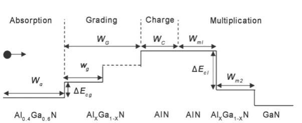
A schematic representation of the conduction band for the proposed SAGCM- APD is illustrated in Figure 1. Thicknesses of the layers constituting the pro-posed device and the band discontinuities at the corresponding hetero interfaces are labeled on the figure. Role of the grading is to overcome the relatively large discontinuity between the conduction bands of Al0.4Ga0.6N and AlN (~1.68 eV),
as well as the lattice mismatch between these two materials. Whereas, the AlN charge layer that is a highly p+ doped thin AlN layer separates the absorption
and multiplication layer, providing high electric field in the multiplication layer and relatively low electric field in the absorption layer.
Using ensemble Monte Carlo (EMC) simulation, we have obtained the opti-mized values for thicknesses of layers constituting the absorption, grading and multiplication regions; as well as the Al mole fraction, x, in various AlxGa1−xN
layers, all of which, in turn, lead to an optimized value for the device excess noise factor. In optimizing the layers thicknesses in the AlN/AlxGa1−xN/GaN
DOI: 10.4236/opj.2017.710015 153 Optics and Photonics Journal
Figure 1. Schematic representation of the conduction band for the proposed
SAGCM-APD (Band discontinuities are drawn not to the scale).
localized as close as possible to both AlN/AlxGa1-xN and AlxGa1-xN/GaN
hete-ro-interfaces, in the multiplication region, but within the narrower hand-gap sides of each interface. In an optimized double heterostructure multiplication region, such as AlN/AlxGa1−xN/GaN, AlN should be thick enough for electrons,
just before crossing over the heterointerface, to have the chance of attaining mean energies, EM-AlN, very close but smaller than their corresponding ionization
threshold energy, ETH-AlN, and yet larger than the carriers’ ionization threshold
energy in the narrower band-gap material; i.e., ETH-AlN> EM-AlN > ETH (AlxGa1-xN).
Hence, such electrons, upon entering AlxGa1-xN, have enough energy to get
in-volved in an II event without a need to traverse the dead space in that region. In this manner the first ionization event is localized to the hetero interface within AlxGa1-xN. In the same manner, AlxGa1-xN also should be thick enough to localize
the next ionization event adjacent to the next heterointerface and yet within the GaN. Eliminating the carriers’ dead spaces in both AlxGa1-xN and GaN regions,
in this manner, reduces the device excess noise factor, in effect.
As we have already mentioned, there is a relatively large band-gap discontinu-ity between the Al0.4Ga0.6N (EG= 4.52 eV) used for the absorption region and
AlN (EG=6.2 eV) as the starting material for the proposed APD structure. For
electrons to overcome such a large barrier height, one needs to use an optimum grading region through which electrons pass with minimal transit time minimal total reflection. In one hand, for electrons to cross over a grading region with minimal reflections number of steps/layer making up the region should be maximized. On the other hand, to keep electrons transit time as short as possi-ble, total thickness of such region should be minimized. Therefore, there are two critical design parameters by which an optimum grading region can be designed. Those are, thickness of each layer, wg, and the barrier (step) height between to
adjacent layers, ΔEcg, through which optimum number layers with optimum
thicknesses can be obtained.
distribu-DOI: 10.4236/opj.2017.710015 154 Optics and Photonics Journal by the Keldysh approach using ionization threshold energy and softness coeffi-cients as fitting parameters to the experimental ionization coefficient data [14]. Multiplication region is divided to 4500 cells and 20,000 super particles are used for simulation. To initiate, an electron is injected to multiplication region. It can drift and scatter in across of the multiplication region. Total careers that reach to both sides of multiplication region are counted. Number of these careers is fined as gain. This process is simulated 20,000 times. Excess noise factor is de-fined by ratio of the average of the square of gains to the square of the gain av-erage [14].
3. Results and Discussion
To validate our MC model, we calculate electron impact ionization coefficients (α) and compare to calculated electron impact ionization coefficients by Bulutay for AlxGa1-xN (x=0, 0.2, 0.4,,1) as shown in Figure 2[14].
As the Al mole fraction is increasing in AlxGa1-xN, electron impact ionization
coefficient is reduced. More Al mole fraction results in the heavier carriers and wider band-gap material. So, the threshold energy for impact ionization and dead space are increased. The obtained threshold energy for electron II has given in Table 1.
According to mentioned modeling, we design and simulate the DH AlN/Al0.4Ga0.6N/GaN multiplication region SAGCM-APD (see Figure 1).
Pho-tons are absorbed in Al0.4Ga0.6N region where distances of photon absorption
from illuminated edge are distributed exponentially. We select Wa= 200 nm
re-sults in more than 90% of entering photons is absorbed in Al0.4Ga0.6N. Details of
different layers are given for proposed SAGCM-APD in Table 2. Wm1 and Wm2
are calculated for different charge layers.
As the length of the grading region shrinks, mean transit time through the barriers reduces and distribution of energy of electrons becomes almost narrow. However, one can shrink grading regions until the electrons can pass the grading region. So, the number of steps (Nstep) and length of the grading region (WG) are
key parameters. We considered the different lengths of grading layer and grad-ing region, which our simulations demonstrated the minimum length of the grading region is 88 nm with Nstep= 9 where electrons could inject to charge
DOI: 10.4236/opj.2017.710015 155 Optics and Photonics Journal
Figure 2. Electron impact ionization coefficients versus
electric field, in AlxGa1-xN, for various x, obtained by
EMC simulation (symbols) compared with calculated results (lines) obtained from Bulutay [14].
Table 1. Threshold energy for electron II events.
Al content (x) in AlxGa1-xN 0 0.2 0.4 0.6 0.8 1
ETH (eV) 4 4.5 5.2 5.7 6.3 6.8
Table 2. Details of the proposed SAGCM-APD.
n+-GaN
Multiplication
[NA = 1016 (cm−3)] Charge 9-steps Grading Absorption
p− GaN p− Al
0.4Ga0.6N p− AlN p+-AlN p−-AlxG1−xN (0.4 ≤ x ≤1) p− Al0.4Ga0.6N
D
N+ W Wm3 Wm2 (nm) Wm1 (nm) NA (1017 cm−3) WC (nm) NA WG NA Wa
2 × 1018 cm−3 30 nm 250 nm
50 78 5 30
1016 cm−3 88 nm 1016 cm−3 200 nm
50 74 4.6 35
48 72 4 40
46 70 3.6 45
46 66 3.1 50
layers and each one step decreasing respectively. As the FWHM is larger, the distribution of energy is more broaden.
To compare different charge layers (that are tabulated in Table 2), we calcu-late FWHM in distribution of energy for electrons at end of the charge region. One can see FWHM is increased ~0.04 ev for each 5 nm increasing in length of the charge layer (see Table 3).
Injected energized electrons from charge to multiplication region need to al-most short dead space to gain the threshold energy for II in AlN. Maximum electric field in multiplication region is lower than 2.7 MV∙cm−1 to breakdown is
[image:5.595.57.549.403.558.2]DOI: 10.4236/opj.2017.710015 156 Optics and Photonics Journal mole fractions.
Existence of an optimum value for Al mole fraction (x) is due to two issues whose effects on δ1 are in opposite direct; 1) reflection from hetero-interface,
and 2) access to more energy due to discontinuity of energy at hetero-interface. In one hand, As the Al content in AlxGa1-xN is reduced, reflection from
hete-ro-interface AlN/AlxGa1-xN is increased. Some reflected electrons can gain the
more energy from electric field to ionize in AlN region. After the ionization event, they have low energy when are injected (transmitted) to AlxGa1-xN region.
Also, scattering processes can reduce the energy of other reflected electrons. So, they need to long dead space to can be ionized in AlxGa1-xN region. This issue
degrades the localization of impact ionization events at near the hetero-interface. On the other hand, As the Al content in AlxGa1-xN is reduced, discontinuity of
energy at hetero-interface is increased. So, the probability of II occurrence for transmitted electrons to AlxGa1-xN is increased and transmitted electrons are
io-nized near the hetero-interface in AlxGa1-xN. Knowing all these, we deduce from
Figure 3, access to more energy due to discontinuity of energy at hetero-interface has dominant effect on reduction of δ1 for x ≥ 0.4 while reflection from
hete-ro-interface increases δ1 for x < 0.4.
After first II events in Al0.4Ga0.6N, electrons with different initial energies drift
to GaN region and can gain the threshold energy to ionization. Figure 4 de-monstrates <δ2> for Al0.4Ga0.6N/GaN with different lengths of Al0.4Ga0.6N region.
One can see the minimum δ2 is obtained when the length of Al0.4Ga0.6N (Wm2)
region is 50 nm. Our simulations demonstrates II events in Al0.4Ga0.6N occur for
Wm2> 50 nm. This issue degrades localization of second II events in GaN for
Wm2> 50 nm, because after II in Al0.4Ga0.6N, electrons have low energy and need
to long dead space to ionized in GaN. Now, we calculate excess noise factor (F) for two different devices: a) a fabricated homojunction Al0.4Ga0.6N pin-APD [4],
and b) our proposed SAGCM-APD with WC= 30 nm (see Figure 5).
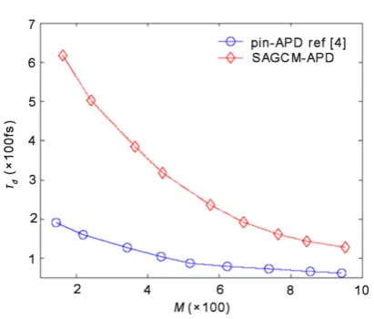
Our simulation demonstrates the proposed SAGCM can reduce excess noise ~64% than a fabricated device for M ≈ 900 [4]. We have calculated the mean time for electrons from generation in absorption region to exit from n+ GaN
re-gion, τd, for two mentioned devices in Figure 6. In high gain regimes, electrons
[image:6.595.208.541.91.128.2]DOI: 10.4236/opj.2017.710015 157 Optics and Photonics Journal
Figure 3. Average distance of first II events in AlxGa1-xN from
[image:7.595.268.478.288.453.2]he-tero-interface AlN/AlxGa1-xN with different Al mole fractions and Wm1 = 78 nm.
Figure 4. Average distance of second II events in GaN from
Al0.4Ga0.6N/GaN hetero-interface with different lengths of Al0.4Ga0.6N
region.
Figure 5. Calculated excess noise factor (F) versus multiplication
(M) for the proposed SAGCM with WC= 30 nm and a fabricated
[image:7.595.268.479.515.681.2]DOI: 10.4236/opj.2017.710015 158 Optics and Photonics Journal
Figure 6. Calculated mean time for electrons from generation in
absorption region to exit from n+ GaN region with different
mul-tiplication factors.
Our simulations demonstrate the delay time for SAGCM is almost reduced exponentially with gain and it’s ~65 fs longer than a fabricated pin-APD [4] for M ≈ 900 while its excess noise is only ~26.6 at this gain. To reduce total noise in system, one employs ADPs in high gain regimes to remove amplifier block after photodetection. So, in high gain applications, the proposed SAGCM device can be used to reduce excess noise mainly.
4. Conclusion
In this study, we presented and designed a wide band gap SAGCM-APD with Al0.4Ga0.6N in absorption region and a DH AlN/Al0.4Ga0.6N/GaN in
multiplica-tion region to reduce excess noise. Our study demonstrated that the large amount of conduction band discontinuity, always, did not enhance localization of impact ionization events near the hetero-interface. In fact, less Al content (x) in AlxGa1-xN (or more discontinuity in AlN/AlxGa1-xN) results in more reflection
which destroys the localization of first impact ionization events in AlxGa1-xN and
has dominant effect on excess noise for x < 0.4. We divided the large discontinu-ity between AlN and GaN in two smaller discontinuities to enhance the first and second localizations. Length of grading layer, number and size of steps in grad-ing layer are key parameters to design. Our simulation demonstrates that one can shrink the length of grading region until 88 nm (with 9 steps) where the car-riers can pass the grading layers. We showed that 30 nm for length and 5 × 10¹⁷
cm−3 for doping concentration of charge layer are good choice. Using these
is-sues, we could mainly reduce excess noise than a fabricated pin-APD for high gains.
References
DOI: 10.4236/opj.2017.710015 159 Optics and Photonics Journal [2] Shen, S.C., Zhang, Y., Yoo, D., Limb, J., Ryou, J.H., Yoder, P.D. and Dupuis, R.D.
(2007) Performance of Deep Ultraviolet GaN Avalanche Photodiodes Grown by MOCVD. IEEE Photonics Technology Letters, 19, 1744-1746.
https://doi.org/10.1109/LPT.2007.906052
[3] Yoo, D., Limb, H., Ryou, J. H., Zhang, Y., Shen, S.C., Dupuis, R.D., Hanser, D., Preble, E. and Evans, K. (2007) AlxGa1-xN Ultraviolet Avalanche Photodiodes
Grown on GaN Substrates. IEEE Photonics Technology Letters, 19, 1313-1315. https://doi.org/10.1109/LPT.2007.902376
[4] Tut, T., Butun, B., Gokkavas, M. and Ozbay, E. (2008) AlxGa1-xN-Based Avalanche
Photodiodes with High Reproducible Avalanche Gain. Physica Status Solidi (C), 5, 2316-2319. https://doi.org/10.1002/pssc.200778735
[5] Tut, T., Butun, B., Gokkavas, M. and Ozbay, E. (2007) High Performance Al
x-Ga1-xN-Based Avalanche Photodiodes, Photonics and Nanostructures—Fundamentals and Applications, 5, 140-144. https://doi.org/10.1016/j.photonics.2007.05.001 [6] David, J.P.R. and Tan, C.H. (2008) Material Considerations for Avalanche
Photo-diodes. IEEE Journal of Selected Topics in Quantum Electronics, 14, 998-1009. https://doi.org/10.1109/JSTQE.2008.918313
[7] Wang, S., Sidhu, R., Zheng, X.G., Li, X., Sun, X., Holmes, A.L. and Campbell, J.C. (2001) Low-Noise Avalanche Photodiodes with Graded Impact-Ionization-Engineered Multiplication Region. IEEE Photonics Technology Letters, 13, 1346-1348. https://doi.org/10.1109/68.969903
[8] Kwon, O.H., Hayat, M.M., Wang, S., Campbell, J.C., Holmes, A., Pan, Y., Saleh, B. E.A. and Teich, M.C. (2003) Optimal Excess Noise Reduction in Thin Heterojunc-tion Al0.6Ga0.4As-GaAs Avalanche Photodiodes. IEEE Journal of Quantum Elec-tronics, 39, 1287-1296. https://doi.org/10.1109/JQE.2003.817671
[9] Chen, J., Zhang, Z., Zhu, M. and Li. X. (2017) Optimization of InGaAs/InAlAs Avalanche Photodiodes. Nanoscale Research Letters, 12, 33-38.
[10] Kleiniw, P., Rutz, F., Aidam, R., Bronner, W., Heussen, H. and Wlther, M. (2015) Charge-Layer Design Considerations in SAGCM InGaAs/InAlAs Avalanche Photo-diodes. Physica Status Solidi (A), 213, 925-929.
https://doi.org/10.1002/pssa.201532556
[11] Huang, J.J.-S., Chang, H.S., Jan, Y.-H., Ni, C.J., Chen, H.S. and Chou, E. (2017) Temperature Dependence Study of Mesa-Type InGaAs/InAlAs Avalanche Photo-diode Characteristics. Advances in OptoElectronics, 46, 132-136.
[12] Wu, Z., Tu, J., Tian, Y., Guo, J. and Zhao, Y. (2017) Time Domain Analysis of Hole Trapping Effect in Avalanche Photodiode Using Schrödinger’s Equation. IEEE Electron Device Letters, 38, 493-496.
[13] Farrel, A.C., Senanayake, P., Hung, C.H., Hovayake, G.E., Rajagopal, A., Currie, M., Hayat, M.M. and Huffaker, D.L. (2015) Plasmonic Field Confinement for Separate Absorption-Multiplication in InGaAs Nanopillar Avalanche Photodiodes. Scientific Reports, 5, 37-39. https://doi.org/10.1038/srep17580
![Figure 2. Electron impact ionization coefficients versus electric field, in AlEMC simulation (symbols) compared with calculated results (lines) obtained from Bulutay xGa1-xN, for various x, obtained by [14]](https://thumb-us.123doks.com/thumbv2/123dok_us/169153.509149/5.595.57.549.403.558/electron-ionization-coefficients-electric-simulation-compared-calculated-obtained.webp)