Planar elliptical solid immersion lens based on a Cartesian oval
D. McCloskey and J. F. Donegan
Citation: Applied Physics Letters 103, 091101 (2013); doi: 10.1063/1.4818781 View online: http://dx.doi.org/10.1063/1.4818781
View Table of Contents: http://scitation.aip.org/content/aip/journal/apl/103/9?ver=pdfcov Published by the AIP Publishing
Articles you may be interested in
Mid-infrared imaging with a solid immersion lens and broadband laser source Appl. Phys. Lett. 90, 121131 (2007); 10.1063/1.2716337
Direct measurement of laser power through a high numerical aperture oil immersion objective lens using a solid immersion lens
Rev. Sci. Instrum. 73, 2011 (2002); 10.1063/1.1470231
Near-field photolithography with a solid immersion lens Appl. Phys. Lett. 74, 501 (1999); 10.1063/1.123168
Raman imaging of patterned silicon using a solid immersion lens Appl. Phys. Lett. 73, 2275 (1998); 10.1063/1.121700
Planar elliptical solid immersion lens based on a Cartesian oval
D. McCloskey1,2,a)and J. F. Donegan1,2 1
School of Physics, Trinity College Dublin, College Green, Dublin 2, Ireland
2
Centre for Research on Adaptive Nanostructures and Nanodevices (CRANN), Trinity College Dublin, College Green, Dublin 2, Ireland
(Received 12 April 2013; accepted 26 June 2013; published online 26 August 2013)
We report on the design of a single element planar solid immersion lens which is theoretically capable of confining light to a focal spot with full width half maximum of 0.29 k (154 nm at
k¼532 nm) and achieving an effective numerical aperture of 1.732. Devices are fabricated and initial optical characterization is performed using a far-field imaging technique providing a lower bound on the numerical aperture of 0.7. Experimental results compare well with two dimensional finite element method simulations. Devices can be mass produced using ultraviolet lithography and produce focal volumes lower than expensive microscope objectives.VC 2013 AIP Publishing LLC.
[http://dx.doi.org/10.1063/1.4818781]
The smallest spot that can be produced by focusing propagating light using free space optics is limited to approx-imately half the wavelength of the incident light by diffrac-tion. Multiple metrics are used to define the diffraction limited spot size. Here, we use the full width half maximum (FWHM) of the square of the Airy function which is given by FWHM¼0.51k/NA. The 1/e2 waist is calculated from this byw1=e2 ¼FWHM
ffiffiffiffiffiffiffiffiffiffi
lnð4Þ
p
. This limit results from the fi-nite aperture of the optics which limits the range of spatial frequencies collected. The key to compressing light further is to include higher spatial frequencies.1 One technique to increase spatial resolution is by taking advantage of evanes-cent components of the field. Surface plasmon polaritons (SPPs) and localized surface plasmons (LSPs) can confine light to deeply sub-wavelength volumes.2–4 Aperture scan-ning techniques such as scanscan-ning near field optical micros-copy (SNOM) can obtain resolutions of 20 nm by placing a metallic antenna in the near-field of the surface under investigation.5–7The efficiency of this technique is however low at 105making it unsuitable for excitation and applica-tions which require high throughput.8For emerging technol-ogies, such as heat assisted magnetic recording (HAMR), it is necessary to create a small excitation focal volume with high power throughput using a compact device, which can be fabricated using standard lithography techniques.9
Solid immersion lenses (SIL) give the possibility to achieve sub-wavelength focal spots while retaining high transmission. An SIL is in general a 3D hemisphere made from a high refractive index material which is placed close to the focal plane of a high NA objective.10These structures bend the incident light to effectively increase the NA of the objective. They have been used to achieve a FWHM of 0.25 k(139 nm @k¼560 nm).11 There are two traditional designs for solid immersion lenses: a hemispherical lens which increases the resolution by a factor of the refractive index (n)10and a super-SIL (Weierstrass geometry) which is capable of increasing the resolution by n2.12These structures are designed to work in conjunction with a high NA focusing
lens in order to increase resolution. When the SIL is index matched and brought in contact with the surface, it is referred to as a numerical aperture increasing lens (NAIL) and allows light which would normally be trapped at the surface by total internal reflection to escape to free space. The NAIL has been used to image integrated circuits with a resolution of 0.23k(230 nm atk¼1lm).13Numerous modi-fications and optimizations have been made on these designs.14,15In practice, it can be difficult to achieve the the-oretical resolution for 3D SILs due to polishing imperfec-tions or inaccurate truncation of the sphere.
Planar solid immersion lenses (PSILs) have been proposed as a method to effectively integrate SILs and to al-leviate alignment issues.16,17 Previous work used standard SIL designs, to create PSILs with spot FWHM of 0.71 k
(453 nm atk¼632.8 nm).17These devices were lossy due to the need for multiple elements. An alternative route is to use reflection instead of refraction. A planar solid immersion mirror (PSIM) was designed which can create a spot size of 0.278 k (180 nm at 650 nm) and is free from chromatic aberration.18,19
Here, we produce a single element planar focusing structure based on refraction capable of producing focal volumes equivalent to a microscope objective of NA¼1.732. The PSIL is fabricated in a 400 nm layer of Si3N4 (n¼2.0) deposited by low pressure chemical vapor
deposition (LPCVD) on a 2lm thick thermal oxide SiO2
(n¼1.4), using electron beam lithography (EBL) and inductively coupled plasma (ICP) etching. The EBL is used in order to facilitate prototyping; however, these structures are large enough to be easily mass produced using UV lithography.
The ideal shape for creating an image without spherical aberration was originally discovered by the famous philoso-pher and mathematician Rene Descartes in 1637, then later studied by Newton in 1664 and Maxwell in 1864 and Huygens.20,21 Specifically the shape can produce two per-fectly conjugated planes and is well known in optical lens design22as a Cartesian oval. This shape was recently demon-strated to create whispering gallery mode resonators with unidirectional emission.23
a)
For the case of an incident plane wave (i.e., object plane at infinity), the equation of the shape in Cartesian coordi-nates reduces to
xa n1 n1þn0
2
a2 n1
n1þn0
2 þ
y2
a2n1n0
n1þn0
¼1: (1)
The origin is taken on the centre line of the first boundary of the shape andais the distance from the origin to the image plane as depicted in Fig.1. n1and n0are the refractive index
of the ellipse and surrounding material, respectively. Comparison with the standard equation for an ellipse with centre M on the x axis and 0 on the y axis,
ðXMÞ2
A2 þ
Y2
B2¼1 (2)
shows that this describes an ellipse with semi-major axis A, semi-minor axis B, and centre M given by
A¼ n1
n1þn0
a; (3)
B¼ n1n0
n1þn0
1=2
a; (4)
M¼ n1
n1þn0
a: (5)
This ellipse has a specific ratio of major to minor axes which depends on the refractive index contrast. The structure thus only depends on one parametera. These elliptical structures will create a focal spot at F2, which is inside the ellipse. Since the focusing effect occurs completely due to refraction at one interface, the ovals can be truncated at F2 without affecting the NA of the structure. The distance from the centre of the ellipse to the truncated surfacefand the length of the chordlare given by
f ¼ n0
n1þn0
a; (6)
l¼ 2ðn 2 1n
2 0Þ
n1ðn1n0Þ
!
a: (7)
For the case of Si3N4in air, n1¼2.0 and n0¼1. This leads
toA¼2=3a, B¼a/pffiffiffi3, f¼a/3, andl¼a. The maximum half angle collected by this structure is hmax¼60 leading to NA ¼nsinðhmaxÞ¼
ffiffiffiffiffiffiffiffiffiffiffiffi n21 p
¼1.732, which is independent ofa. A simple far-field imaging technique depicted in Fig.
[image:3.612.64.283.54.230.2]2(a) is used to experimentally investigate the focusing
FIG. 1. Schematic of Cartesian oval for focusing collimated light. Truncated region is shaded in grey. Light is indent from the left and focused to a point at F2. F1 and F2 are the foci of the ellipse. The major axis A and minor axis B are shown. The oval is centered at M on the x-axis, with the origin o at the first interface. The parameterlis the length of the chord when the oval is truncated through the second focus. The parameterfis the distance from the center of the oval to the truncated boundary.
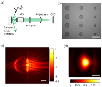
FIG. 2. (a) Experimental setup: Linearly polarized light from a 532 nm DPSS laser is introduced at an angle of 80to normal. The polarization is con-trolled to be either s or p polarized with respect to the substrate. The scat-tered light is collected with a NA¼0.7 100Mitutoyo long working distance objective and imaged onto a CCD at 100 magnification using a 200 mm focal length lens. (b) Optical micro-graph of typical array. Four repeats of
a¼20lm, a¼15lm, and a¼10lm are shown. Scale bar: 50lm. (c) Experimental image on log scale showing near-field intensity distribu-tion. Oval with a¼10lm, incident light p-polarized at 532 nm. Scale bar: 5lm. (d) Close up of focal spot on lin-ear scale. FWHM of spot size is 420646 nm, diffraction limited by the collection objective (NA¼0.7). Scale bar: 500 nm.
[image:3.612.49.375.494.773.2]properties of these structures. Light from a 3.2 mW CW diode pumped solid state (DPSS) laser with wavelength of 532 nm is incident at 80to the substrate normal. The beam is spatially filtered to give a Gaussian profile with 1.5 mm 1/e2 diameter. This effectively creates a plane wave excitation on the scale of a single scatter. The incident light is controlled to be s-polarized or p-polarized with respect to the substrate. The ovals are imaged from above using a 0.7 NA long work-ing distance microscope objective. Only light which is scat-tered by the structures into the 45half angle collection cone of the objective is collected. The resulting image is a spatial map of the origin of the scattered light which is related to the local intensity. Secondary scattering from the SiO2substrate
creates signal which is two orders of magnitude weaker, giv-ing a map of the local intensity distribution outside of the structure.24A linear polarizer can be placed after the objec-tive to analyze the polarisation of the scattered light. A typi-cal array of fabricated structures is shown in Fig.2(b)under 50magnification. In order to record signal from both scat-tering processes, the dynamic range of the CCD is extended by taking four images with different gain and shutter settings and adding them after calibration. An experimental image of a truncated oval with a¼10lm,k¼532 nm, and p-polarized
input light is shown on log10scale in Fig.2(c). There is detail
in the image over 3 orders of magnitude.
[image:4.612.51.407.348.768.2]A close up of the focal region is shown on a linear scale in Fig.2(d). The spot is blurred to a FWHM of 420646 nm by the point spread function (PSF) of the collecting objective (FWHM 390 nm, with NA¼0.7). The near-field intensity distribution is calculated numerically for a 2D structure with the same cross section and an index of 2 using the finite ele-ment method (COMSOL). The light is known to be confined to the 400 nm layer in the out of plane direction from previ-ous work24 putting an upper limit on the spot waist of 200 nm for this case; however, these structures are too large for full 3D numerical simulation. A comparison of numerical results with the experimental images shows that the scattered light retains the polarization properties of the near-field com-ponents. Figures 3(a)–3(c) are experimental results with no analyzer and with analyzer polarized along x-axis and y-axis, respectively. The incident light is s-polarized (along y-axis.). Figs. 3(d)–3(f) show the 2D FEM calculated total near-field intensity, jExj2 and jEyj2, respectively. The focal spot is larger for s-polarized light (320 nm) than p-polarized light (154 nm). This is due to the discontinuity of electric field at the interface of the structure in the s-polarized (TE)
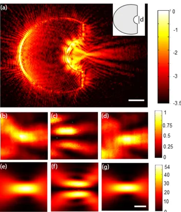
FIG. 3. 2lm2lm close-up of region around the focus for a truncated oval with a¼15lm. All images are on a linear scale for s-polarized case. The top row figures are normalized experi-mental measurements with (a) no ana-lyzer, (b) x-polarized, and (c) y-polarized. The second row figures are results of 2D FEM with (d) total field, (e)jExj2, and (f) jEyj2, normalized to
the incident intensity. (g) Plot showing linear relationship of focal intensity to
case. The experimental results verify that the PSILs are capa-ble of focusing light at least as tight as a microscope objec-tive with NA¼0.7. Higher resolution methods for mapping the near-field such as SNOM are necessary to see the actual spot size and are currently underway. The intensity enhance-ment is linear with the parameter a (Fig. 3(g)). Since the focal spot size is independent of a, the structures can be designed for a specific intensity enhancement to suit a partic-ular application.
The Cartesian oval works by converting a plane wave into a cylindrical wave which converges to a point at F2. Since the cylindrical wavefront is created by refraction at the first interface alone, a cylinder with diameter dcan be cut into the structure centred on the point F2 as shown inset in Fig.4. The wavefront will be parallel to this interface and will not undergo refraction, minimising distortion to the focal spot. The oval now acts as a high NA lens with a Gaussian focus outside of the structure which is not in con-tact with the interface. An experimental image of focusing by a truncated oval with parametera¼20lm and a cylindri-cal cut out withd¼10lm is shown on log scale in Fig.4(a). Controlling the ratio of the diameter of this cut-out to the size parameter of the ovalaallows control over the effective
NA of the structure and the spot size. The maximum inten-sity in the focal region Imaxand the effective NA of the oval
calculated from FEM are tabulated for different values of a
anddin Table.I. Whendis comparable witha, the length of the refracting interface is shortened resulting in a lower NA. When d<k, additional confinement results in a higher effective NA.
A design of planar solid immersion lens is presented. The structure is capable of creating an effective NA of
FIG. 4. (a) Experimental image of fo-cusing by a truncated oval with param-eter a¼20lm and a cylindrical cut out with d¼10lm is shown on log scale. Incident light is s-polarized (along y-axis). Inset showing parameter d. (b) Normalized experimental intensity map for a 2lm2lm region around the focal region with no analyzer, (c) with analyzer polarized along x-axis, and (d) with analyzer polarized along y-axis. (e) Results of 2D FEM simula-tion of near field intensity for total field, (f) for x-componentjExj2, (g) for
[image:5.612.51.404.48.462.2]y-componentjEyj2.
TABLE I. Maximum intensity Imaxand effective NA tabulated for different
aandd.
a (lm)
Imax/NA 4 6 8 10 15 20
d (lm) 0.2 17/1.65 26/1.54 33/0.89 40/1.7 58/0.95 75/0.89 0.5 13/0.92 19/0.93 26/0.68 34/0.92 46/0.75 61/0.72 1 12/0.78 18/0.77 22/0.77 28/0.77 42/0.74 56/0.7 2 12/0.77 18/0.79 22/0.77 28/0.82 42/0.73 54/0.68 5 11/0.77 18/0.76 22/0.77 29/0.79 43/0.72 57/0.68 10 10/0.55 22/0.75 28/0.77 44/0.74 54/0.67
[image:5.612.315.561.657.770.2]ffiffiffiffiffiffiffiffiffiffiffiffiffi n21 p
using a single element and without the need for a focusing lens. These structures are fabricated in Si3N4 and
shown numerically to produce a focal spot with FWHM of 154 nm atk¼532 nm equivalent to an NA of 1.732. A far-field imaging method confirms the spot size is smaller than 420646 nm (NA¼0.7). Modifying the structure allows access to the focal area and control over the spot size and NA. These structures can be mass produced using standard lithog-raphy processes. We have outlined a design to produce these structures in any material system. It is possible to investigate solutions using water as a cladding layer. Use of even higher index materials such as gallium phosphide and shorter wave-lengths could produce focal spots with FWHM as small as 87 nm at k¼560 nm. (effective NA¼3.27). These devices will find uses as focusing elements for biological sensing, flu-orescence correlation spectroscopy (FCS), single molecule excitation, optical recording, optical lithography, and heat assisted magnetic recording. Further work is underway to confirm the spot size using near-field methods and to optimise the materials and thickness of the guiding layer.
The authors would like to thank K. E. Ballantine and P. R. Eastham for useful discussions, and P. Gleeson and N. O’Hara for etching expertise. This work was supported by Science Foundation Ireland (SFI) under Grant No. 08/IN.1/ I1862.
1L. Novotny and B. Hecht, Principles of Nano-Optics (Cambridge
University Press, Cambridge, 2006).
2
L. Feng, K. A. Tetz, B. Slutsky, V. Lomakin, and Y. Fainman,Appl. Phys. Lett.91, 081101 (2007).
3Z. Liu, J. M. Steele, W. Srituravanich, Y. Pikus, C. Sun, and X. Zhang, Nano Lett.5, 1726 (2005).
4
L. Yin, V. K. Vlasko-Vlasov, J. Pearson, J. M. Hiller, J. Hua, U. Welp, D. E. Brown, and C. W. Kimball,Nano Lett.5, 1399 (2005).
5H. G. Frey, F. Keilmann, A. Kriele, and R. Guckenberger,Appl. Phys. Lett.81, 5030 (2002).
6
U. Durig, D. W. Pohl, and F. Rohner,J. Appl. Phys.59, 3318 (1986).
7A. Harootunian, E. Betzig, M. Isaacson, and A. Lewis,Appl. Phys. Lett. 49, 674 (1986).
8
L. P. Ghislain, V. B. Elings, K. B. Crozier, S. R. Manalis, S. C. Minne, K. Wilder, G. S. Kino, and C. F. Quate,Appl. Phys. Lett.74, 501 (1999).
9T. Rausch, C. Mihalcea, K. Pelhos, D. Karns, K. Mountfield, Y. A.
Kubota, X. Wu, G. Ju, W. A. Challener, C. Peng, L. Li, Y.-T. Hsia, and E. C. Gage,Jpn. J. Appl. Phys., Part 145, 1314 (2006).
10
S. M. Mansfield and G. S. Kino,Appl. Phys. Lett.57, 2615 (1990).
11Q. Wu, G. D. Feke, R. D. Grober, and L. P. Ghislain,Appl. Phys. Lett.75,
4064 (1999).
12
B. D. Terris, H. J. Mamin, and D. Rugar,Appl. Phys. Lett.68, 141 (1996).
13
S. B. Ippolito, B. B. Goldberg, and M. S. U€unlu€u,Appl. Phys. Lett.78, 4071 (2001).
14Y. Zhang,Appl. Opt.
45, 4540 (2006).
15
V. V Kotlyar, A. A. Kovalev, and A. G. Nalimov,Optics1, 1 (2012).
16
D. Intani, T. Baba, and K. Iga,Appl. Opt.31, 5255 (1992).
17D. Chien, C. Tsai, S. Lo, C. Chen, and J. Chang,J. Lightwave Technol. 23, 2746 (2005).
18
C. Peng, C. Mihalcea, K. Pelhos, and W. A. Challener,Appl. Opt.45, 1785 (2006).
19W. A. Challener, C. Mihalcea, C. Peng, and K. Pelhos,Opt. Express13,
7189 (2005).
20
J. P. C. Southall, Aplanatic (or Cartesian) Optical Surfaces (J. B. Lippincott, 1922).
21R. K. Luneburg,Mathematical Theory of Optics(University of California
Press, Berkeley, 1964).
22
D. Michaelis, P. Schreiber, and A. Br€auer,Opt. Lett.36, 918 (2011).
23
Q. J. Wang, C. Yan, N. Yu, J. Unterhinninghofen, J. Wiersig, C. Pfl€ugl, L. Diehl, T. Edamura, M. Yamanishi, H. Kan, and F. Capasso,Proc. Natl. Acad. Sci. U.S.A.107, 22407 (2010).
24