LEABHARLANN CHOLAISTE NA TRIONOIDE, BAILE ATHA CLIATH TRINITY COLLEGE LIBRARY DUBLIN OUscoil Atha Cliath The University of Dublin
Terms and Conditions of Use of Digitised Theses from Trinity College Library Dublin
Copyright statement
All material supplied by Trinity College Library is protected by copyright (under the Copyright and Related Rights Act, 2000 as amended) and other relevant Intellectual Property Rights. By accessing and using a Digitised Thesis from Trinity College Library you acknowledge that all Intellectual Property Rights in any Works supplied are the sole and exclusive property of the copyright and/or other I PR holder. Specific copyright holders may not be explicitly identified. Use of materials from other sources within a thesis should not be construed as a claim over them.
A non-exclusive, non-transferable licence is hereby granted to those using or reproducing, in whole or in part, the material for valid purposes, providing the copyright owners are acknowledged using the normal conventions. Where specific permission to use material is required, this is identified and such permission must be sought from the copyright holder or agency cited.
Liability statement
By using a Digitised Thesis, I accept that Trinity College Dublin bears no legal responsibility for the accuracy, legality or comprehensiveness of materials contained within the thesis, and that Trinity College Dublin accepts no liability for indirect, consequential, or incidental, damages or losses arising from use of the thesis for whatever reason. Information located in a thesis may be subject to specific use constraints, details of which may not be explicitly described. It is the responsibility of potential and actual users to be aware of such constraints and to abide by them. By making use of material from a digitised thesis, you accept these copyright and disclaimer provisions. Where it is brought to the attention of Trinity College Library that there may be a breach of copyright or other restraint, it is the policy to withdraw or take down access to a thesis while the issue is being resolved.
Access Agreement
By using a Digitised Thesis from Trinity College Library you are bound by the following Terms & Conditions. Please read them carefully.
N an o p a ttern in g m agn etic m aterials -
C r /M o (1 1 0 ) ep itaxial sy stem and
Fe
3 0 4
( l l l ) surface
A thesis subm itted to the University of DubHn, Trinity College,
in application for the degree of Doctor in Philosophy
by
A lexan d ru C azacu
Physics Departm ent
Trinity College Dublin
TRINITY COLLEGE
I
D eclaration
This thesis is subm itted by the undersigned for the degree of Doctor in
Philosophy at the University of Dublin.
It has not been subm itted as an exercise for a degree at any other university.
A part from the advice, assistance and joint effort mentioned in the
acknowledgements and in the text, this thesis is entirely my own work.
I agree th at the library may lend or copy this thesis freely on request.
A ckn ow led gem ent s
II
I would first like to th a n k my supervisor Prof. Igor Shvets for giving me the o pp ortunity to work in the field of surface science. He has given me critical guidance during th e course of the project. His determ ination and h ard work were always very m otivating.
I would like to th a n k Dr. Shane M urphy for his generous support, advises and optim ism th rou gh ou t th e project. His continuous interest and confidence helped me to go th rough th e rough times.
I would like to th a n k Sergio Ceballos, Ken Jordan and G iuseppe Manai for their friendship and th e good mom ents. All the past and current people in the group have m ade life b e tte r by their presence, so thanks to: Guido, Nikolay, Victor, M aia, Sumesh, Rom an, W illiam , D iarm aid, Anselm, D im itri, Vivienne, Sunil, Jin, Yang, Kevin, Antony, C iaran, Floriano, Rafa and Keith.
I’d like to th an k M arie for the m any letters and perfect handling of ad m inistrative papers. T he group could not operate w ithout th e efforts of all the departm ental staff; John Kelly, Mic Reilly, Joe McCauley, Chris Smith, Ken Concannon and all the secretarial staff, especially Susan.
Thanks to all my friends, especially N icoleta and Cornel. I would also like to th an k Rev. Dr. Irineu C raciun and Niam h for their warm support.
Ill
IV
A bstract
This thesis presents the investigation of the C r/M o(110) epitaxial inter face. The study combines experim ental techniques in the form o f scanning tunneling microscopy (STM ), low energy electron diffraction (LEED), and Auger electron spectroscopy (AES) and theoretical investigations by means of first-principles density functional theory (D P T ). The C r/M o(110) system is compared w ith the closely related F e/M o(110), C r/W (1 1 0 ), and F e/W (110) system s.
V
surface is compared with th a t on the vicinal Mo(llO) surface. It is found
th a t nanowedges formed on the vicinal surface are typically much thicker,
with smaller lateral dimensions, and have a higher density compared to the
low-index surface.
The (111) surface of m agnetite has also been studied. The formation of
a nanoscale hexagonal pattern by light oxidation of the (111) surface of a
magnetite single crystal is studied using STM and scanning tunneling spec
troscopy (STS) measurements in the tem perature range 85 < T < 300 K. The
formation of the pattern is sensitive to surface stoichiometry. STM images
of the surface are strongly bias dependent and the p attern is stable on the
surface from RT to 85 K, which lies below the Verwey transition tem perature
VI
P u b lication s
s . Murphy, A. Cazacu, N. Berdunov, I. V. Shvets, and Y. M. Mukovskii. ’’Nanoscale pattern form ation on the Fe3 0 4( l l l ) surface” . J. Magn. Magn. M a t t , 290-291 (2005) 201-204.
A. Cazacu, S. Murphy, and I.V. Shvets. ’’E pitaxial growth of ultrathin Cr films on M o(llO ) at elevated tem perature” , Phys. Rev. B 73, 045413 (2006).
A. Cazacu, S. Murphy, and I.V. Shvets. "Epitaxial growth of Cr ultrathin films on vicinal and Low Index M o(llO ) surfaces” , Jpn. J. Appl. Phys., Vol. 45, No. 3B, in press, (2006).
P resen ta tion s
” Nanoscale pattern form ation on the Fe3 0 4( l l l ) surface” , A. Cazacu, S. Murphy, N. Berdunov, and I. V. Shvets. Poster presentation at the Joint European M agnetic Sym posium (JEM S’05), Dresden, Germany, Septem ber 2004.
VII
VIII
List o f abb reviations
ID - one dimensional
2D - two dim ensional
3D - three dim ensional
AES - Auger electron spectroscopy
BZ - Bales-Zangwill
CA-PZ - Ceperley Adler-Perdew Zunger
CMA - cylindrical m irror analyser
DOS - density of states
D FT - density functional theory
e-beam - electron beam
ECG - electrostatic centre of gravity
FEEM - field emission electron microscopy
FIM - field ion microscopy
FP-LM TO - full potential-linear muffin tin o rbital
GGA - generalized gradient approxim ation
ES - Ehrlich-Schwoebel
E T - elevated tem perature
FM - Frank van der Merwe
F P -L A P W - full-potential linearized augm ented plane wave
HEIS - high energy ion scattering (spectroscopy)
L - Langmuir
LBL - layer-by-layer
LDA - local density approximation
LDOS - local density of states
LEED - low energy electron diffraction
LT - low-temperature
LTSTM - low-temperature scanning tunneling microscopy
MBE - molecular beam epitaxy
ML - monolayer
PBE - Perdew-Burke-Ernzerhof
FED - photoelectron diffraction
RT - room temperature
RTSTM - room-tem perature scanning tunneling microscopy
SPM - scanning probe microscopy
SPSTM - spin polarised scanning tunneling microscopy
SMOKE - surface magneto optic kerr effect
SK - Stranski-Krastanov
STM - scanning tunneling microscopy
STS - scanning tunneling spectroscopy
SXRD - surface x-ray diffraction
TEM - transmmission electron microscope
TPD - tem perature programmed desorption
TSP - titanium sublimation pump
UHV - ultra high vacuum
VTSTM - variable tem perature scanning tunneling microscopy
VW - Volmer-Weber
List o f Figures
2.1 Schematic illustration of m ajor kinetic processes occuring dur
ing growth from the v a p o r ...
8
2.2 Schematic illustration of the exchange mechanism which may
occur during adatom d iffu sio n ... 10
2.3 Schematic representation of idealized growth regimes in ho
moepitaxy ... 13
2.4 Simplified potential energy surface for adatoms near steps
. .
15
3.1 Top view of the UHV system
... 21
3.2 Schematic of the resistive h e a te r ... 25
3.3 Schematic illustration of the e-beam h e a te r ... 26
3.4 Schematic of four-grid optics in LEED m o d e ... 29
3.5 Schematic representation of a STM tunneling junction . . . .
31
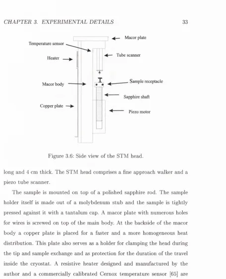
3.6 Side view of the STM h e a d ... 33
3.7 Cross section of the fine approach w a lk e r ... 34
3.8 Schematic illustration of a variable tem perature S T M ... 37
3.9 Temperature dependence of the STM head on t i m e ... 38
4.1 Schematic view of the Mo(llO) atomic s tr u c tu r e ... 43
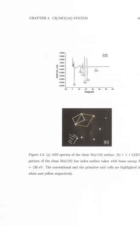
4.2 AES and LEED analysis of the clean Mo(llO) samples . . . .
46
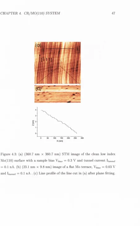
4.3 STM images of the clean low index Mo(llO) s u rfa c e ... 47
L IS T OF FIGURES
XII
4.4
STM image of the clean vicinal Mo(llO) s u r f a c e ... 48
4.5
Cr and Mo concentrations calculated from Auger spectra as a
function of Cr film c o v e r a g e ... 51
4.6
LEED patterns obtained from Cr films of varying coverages
0.11 < 0rfep < 3 ML ... 52
4.7
LEED patterns obtained from Cr films of varying coverages
2.9 <
Bdep <
4.64 M L ... 53
4.8
Submonolayer growth of Cr on Mo(llO) at 420 K
... 58
4.9
STM image of submonolayer Cr film grown at 500 K ... 60
4.10 Submonolayer growth of Cr on Mo(llO) at 575 K
... 64
4.11 Growth of Cr monolayers on Mo(llO) at 575 K
... 65
4.12 Roughness of Cr nanostripes as a function of nanostripe cov
erage on atomic te rrra c e s ... 66
4.13 Stranski-Krastanov regime in Cr films on Mo(llO) at ET . . . 69
4.14 STM image of a 5.2 ML Cr film showing the change in Cr
islands morphology as a function of step o rie n ta tio n ... 70
4.15 Incomplete Cr layers on the Cr nanowedge is la n d s ... 74
4.16 STM image of Cr overlayers on Mo(llO) -
Ocr =
4.6 ML, T^ep
= 400 K ... 75
4.17 STM images of Cr overlayers on the vicinal M o(llO) surface,
0.14 < 6»cr < 3 M L ... 77
4.18 STM images of Cr overlayers on the vicinal Mo(llO) surface,
3.48 <
9cr <
4.64 M L ... 78
5.1
Schematic illustration of the surface relaxation model of Finnis
and H e i n e ... 84
5.2
Vacuum slabs used to model the Mo(llO) substrate and the
L IS T OF F IG U RE S XIII
5.3 Schem atic illustration of th e two fractional steps fi and fg • . . 94 5.4 Experim ental values of the interlayer separation in
Cr/M o(110) system in the submonolayer r e g i m e ... 96 5.5 Experim ental values of the interlayer separation in
C r/M o (110) system for monolayer c o v era g e... 97
6.1 STM images showing the onset of a 2D dislocation network in Cr i s l a n d s ... 108 6.2 STM images showing the sym m etry of th e dislocation p attern 111 6.3 STM images of Cr films illustrating the layer-dependent strain
relaxation p ro c e s s e s ... 113 6.4 STM images showing the dislocation p attern on islands with
different m o r p h o lo g y ... 115 6.5 Local plane fitted STM image of the (110) surface of Cr is la n d s ll6 6.6 STM images illustrating the room tem peratu re growth of frac
tional Fe and Cr film on a predeposited Cr film on M o(llO) . 118 6.7 Histograms showing th e size distribution of Fe islands formed
on the strained Cr bilayer and on the relaxed Cr layers . . . .1 2 0 6.8 STM images illustrating the nucleation of Cr or Fe adatom s
a t room tem p erature on the dislocation p a t t e r n ... 121 6.9 Surface reactivity of Cr monolayers on M o ( l l O ) ...122 6.10 Surface reactivity of Fe monolayers on M o(llO ) ...124 6.11 Density of states of Cr and Fe monolayers on M o(llO) . . . . 125
L IS T OF FIG URE S XIV
7.5 STM images of the superstructure d o m a in s... 138 7.6 STM images of the superstructure domain obtained with dif
ferent bias v o lt a g e s 140
7.7 STM images of the patterned magnetite (111) surface taken at 95 K ...141 7.8 Tunneling spectra of the patterned magnetite (111) surface
taken at different sample te m p e r a tu r e s... 144
List o f Tables
3.1 Resonance frequencies of the piezo s c a n n e r ... 35
4.1 Structure and surface free energy of various metals ... 40
4.2 Details of the deposition parameters and the degree of con
tam ination of chromium films grown on the low index surface
49
4.3 Charasteristics of the Cr nanowedge islands on the low index
Mo(llO) substrate for varying c o v e ra g e ... 71
4.4 Details of the deposition characteristics of Cr films grown on
the vicinal Mo(llO) surface ... 76
4.5 Characteristics of the Cr nanowedge islands on the vicinal
Mo(llO) surface for varying film coverage... 79
5.1 Relaxation of the outermost layer of the ions for low index
planes of different metal structures... 83
5.2 Interlayer separation in the Cr/Mo(110) and Fe/Mo(110) sys
tems calculated using GGA-PBE fu n c tio n a ls ... 100
5.3 Interlayer separation in the Cr/Mo(110) and Fe/Mo(110) sys
tems calculated using LDA-CA-PZ fu n c tio n a ls ... 101
6.1 Layer dependent strain relaxation in Cr nanow edges... 114
C ontents
1
In trod u ction
1
2
B asic principles o f ep ita x ia l grow th
5
2.1
Thermodynamic growth modes ...
5
2.2
Growth k in e tic s ...
8
2.3
Growth modes in hom oepitaxy... 12
2.4
The step edge b a r r ie r ... 14
2.5
Surface s t r e s s ... 15
2.6
Misfit dislocations in epitaxial layers ... 16
3
E xp erim en tal details
20
3.1
The ultrahigh vacuum set u p ... 20
3.2
The preparation ch am b er... 22
3.2.1
The ion g u n ... 23
3.2.2
The resistive h e a te r ... 24
3.2.3
The e-beam h e a t e r ... 25
3.2.4
The e-beam e v a p o ra to r... 27
3.3
Auger electron spectroscopy ( A E S ) ... 28
3.4
Four-grid low energy electron diffraction (LEED) ... 28
3.5
Scanning tunneling microscopy (STM) ... 30
CONT ENT S
XVII
3.6 STM s e t - u p ... 32
3.6.1 STM operation at low te m p e r a tu r e ... 36
4
C r /M o (1 1 0 ) sy stem
39
4.1 In tro d u c tio n ... 39
4.2 Sample p re p a ra tio n ... 44
4.3 Cr films on the low index Mo(llO)
...48
4.3.1 LEED and A E S ... 50
4.3.2 STM results - submonolayer g ro w th ... 57
4.3.3 Monolayer coverage... 62
4.4 Stranski - Krastanov growth re g im e ... 68
4.5 Cr films on the vicinal Mo(llO) s u rfa c e ... 73
4.6 C o n clu sio n s... 80
5
Surface relaxations
81
5.1 In tro d u ctio n ... 81
5.2 Calculation m e th o d ... 87
5.3 Calculation d e t a i l s ... 90
5.4 Multilayer relaxations of the Cr/Mo(110) and Fe/Mo(110) epi
taxial in te rfa c e s... 93
5.5 C o n clu sio n s...104
6
Strain relaxation
105
CONT ENT S XVIII
7 N an oscale p a ttern on th e Fe3 0 4
( l l l ) surface
128
7.1 In tr o d u c tio n ...1287.2 T he (111) surface of m a g n e tite ...131
7.3 Sample p r e p a r a tio n ...134
7.4 Nanoscale pattern form ation on the Fe3 0 4( l l l ) surface . . . . 135
7.5 Scanning Tunneling Spectroscopy (STS) o f the patterned mag
netite (111) s u r f a c e 143
7.6 C o n c lu s io n s ...145
8 Sum m ary and ou tlook
146
C hapter 1
In troduction
Interest in nanoscale p attern s has gathered m om entum in recent years, both in response to th e increasing dem ands for m iniaturization in high-tech ap plications and due to novel properties exhibited by ordered m aterials [1]. Nanoscale p attern in g by self-assembly is viewed to be an attractiv e alterna tive to lithography, which is extrem ely costly when m aking low-dimensional
structures. Such nanoscale p attern s can be obtained by correct tun in g of de position param eters during th e grow th of u ltrath in films. This thesis aims to give some exam ples of n an op attern in g of m agnetic m aterials using th e novel C r/M o(110) epitaxial system and th e (111) surface of m agnetite.
Surfaces and u ltrath in films of 3d m etals have been of much interest be cause of the low dim ensionality effects on electronic and m agnetic properties, notably the considerable enhancem ent of m agnetic mom ent. For exam ple in the case of chromium, th e (110) surface was predicted to have an enhanced m agnetic m om ent of 2.49 j i B i four tim es th e value for the bulk m agnetic m om ent (0.59 /^b) [2]. The Cr(lOQ) surface has been suggested to have ferro m agnetic order despite the bulk antiferrom agnetism [3]. Spin polarised STM
experim ents have shown th a t on th e Cr(OOl) terraced surface there is an
C H A P TE R 1. INT R OD U C TION 2
antiferromagnetic coupling between successive atomic terraces [4].
In addition, in systems with large lattice mismatch, the elastic strain
dram atically affects the charge transfer, the magnetic moments and the ori
entation of the magnetic easy axis. The new structures have unexpected
properties, very different from their bulk counterparts. By controlling the
lattice mismatch, film thickness and deposition parameters, these materials
can be engineered on the nanometer scale. A rich variety of novel proper
ties th a t have been found recently in the case of Fe/W and Fe/Mo epitaxial
systems [5-11].
Since the magnetic properties are closely related to the interatomic bond
length, coordination numbers and symmetry it is of great importance to study
in detail the films morphology, multilayer relaxation and strain relaxation
processes in the low coverage regime of the magnetic/paramagnetic interfaces.
A good example of strong correlation between the particular film morphology
and the magnetic properties is the case of the unconnected Fe islands on
W (llO ) which are superparamagnetic, while island coalescence triggers the
onset of ferromagnetic order through magnetic percolation [5]. It has been
found recently th a t even slight variations of island shape may lead to different
magnetic properties. The magnetization switching behavior of Fe islands on
Mo(llO) is found to occur at higher rates for elongated islands than for
compact ones, which are more robust againt thermal magnetization reversal
[6].
This thesis focuses on the growth mechanisms and relaxation processes of
direc-C H A P T E R 1. I N T R O D U direc-C T I O N 3
tions [16]. SDW o f Cr films have been a subject of intensive research over the last decades [17]. Cr has been studied very little in conjunction with refractory m etal surfaces. So far, STM studies o f the C r/W (110) epitaxial system have been lim ited to the observation o f anisotropic submonolayer growth at room tem perature [12]. Experimentally, Cr coated W tips have been employed to perform spin polarized STM m easurem ents o f Fe bilayers on W (llO ) [13]. The growth of Cr films on stepped W (llO ) and W(OOl) was first studied by Shinn et al. using a com bination o f FEM , LEED, AES, T P D and work function m easurem ents [14,15].
C r/M o(110) has been studied to a far lesser extent and has not been studied before by STM . Theoretical studies o f ultrathin Cr films on M o(001) by Niklasson et al. [18] using first-principles density-functional calculations have indicated that the bare C r/M o(001) exhibits spin-polarized behavior. The spin m oment o f a single Cr monolayer on Mo exhibit a m agnetic m oment of 1.3 //e /a t o m and appreciable induced m agnetic m oment of 0.2 //s /a to m is calculated in the M o(100) topm ost layer which is antiferrom agnetically coupled with the Cr monolayer.
C H AP T ER 1. I NT RO DU C TI ON
C hapter 2
B asic principles o f ep itaxial
grow th
2.1
T h erm odynam ic grow th m odes
Epitaxy describes the growth of a crystalline layer upon (epi-) a crystalline substrate. In epitaxy, the crystalline orientation of the substrate induces an order on the orientation of the deposit layer {-taxis, from the Greek tassein, to arrange). The layer orientation is selected by the m inim ization of the interface energy. Interface energy is related to the adhesion between the film and substrate. It is the energy required to create an interface, which involves destroying two surfaces. If the m aterials are different, the term heteroepitaxy is used while the growth of a crystalline layer on a chem ically identical, crystalline substrate is called homoepitaxy. In heteroepitaxy the interface energy is governed by the adhesive energy as well as by the lattice m ism atch between the substrate and deposit m aterial.
Ernst Bauer [19] introduced in 1958 a classification of epitaxial growth based on therm odynam ic considerations which applies to growth near
C H A P T E R 2. B A S IC P R IN C IP L E S OF E P IT A X IA L G R O W T H 6
m odynam ic equilibrium , th a t is high substrate tem perature and low depo sition flux. Therm odynam ical trea tm e n t is based on a specific surface free energy 7, which is the reversible work per unit area required to create a surface (after Gibbs, [20]). Different growth modes may be distinguished ac cording to the balance between the surface free energy j p of the film, th e surface free energy of th e su b strate 7 5 and the interface free energy jint- The interfacial energy is defined according to the Dupre relation:
lint = 7 S — 7f ~ (^SD (2.1)
where Ps d is free energy of adhesion which represents the work required to separate the su b strate and deposit crystals in their original orientation and w ith the actual atom ic distances [21]. For the case
A7 = 7 f + 7int - 7 s > 0 (2.2)
the energy balance requires to minimize the area covered by the deposit, and the film will grow in th e form of three dimensional islands (3D) on the su bstrate. This mode is nam ed Volmer-Weber (V W ) growth. If
A7 = 7 f + 7int - 7 s < 0 (2.3)
the energy balance requires to maximize the area covered by the deposited m aterial and th e films grow smoothly, one atomic layer at a time. This grow th scenario is known as Frank-van-der-Merwe (FM) or layer-by-layer mode (LBL).
In heteroepitaxy there is a lattice mism atch between the film and sub strate. In th e initial grow th sta te th e film is elastically strained to store the elastic energy. Considering the n-th layer as a new substrate, the chemical influence of th e original su b strate is largely reduced, and the surface free en
C H A P T E R 2. B A S I C P R IN C IP L E S O F E P IT A X IA L G R O W T H 7
substrate im posing a strained n-th layer will give rise to a positive interface energy between layer n and n + 1 which invalidates the condition (2.3) and leads back to the case (2.2). Beginning with the deposition of the layer n + 1, 3D islands will form on top of the n sm oothly grown layers. This growth scenario defines the Stranski-Krastanov (S K ) growth.
J. H. van der Merwe generalized Bauer’s formulation to include the effects of la ttice misfit induced strain [22,23]. T he total interface energy per unit area is a result o f the specific chemical interaction between film and substrate and the elastic strain contribution:
+ j = l , . . . n (2.4)
where e is the strain energy and j is the layer number. The total energy balance for heteroepitaxial system s for layer n can be written as
^ E p + Ej — E s (2.5)
j = i
CHAPTER 2. BASIC PRINCIPLES OF EPITAXIAL G ROW TH 8
re-ev ap o ratio n
n u clea tio n - w
I X l
Interdiffusion s te p
incorporation
deposition
0
1
diffusion
s te p - e d g e diffusion
O Q O -O
island growtti Figure 2.1: Schematic illustration of major kinetic processes occuring during growth.epilayers become unstable at a critical thickness h = he and strain relief occurs by the introduction of misfit dislocations.
The films growth is a combination of energetic and kinetic effects. Ener getic effects (e.g., due to both elastic energy and differences in surface free energies) are prevalent near thermal equilibrium. Kinetic effects (e.g. surface diffusion) are prevalent far from equilibrium i.e. high deposition rate and low substrate temperature. Generally, the two contributions can be separated.
2.2
G row th kinetics
C H APTER 2. B A SIC PRIN C IPLES OF E P IT A X IA L G RO W TH
9
First, their kinetic energy (Efcm) is transferred during the collision to the sub
strate, characterized by the cohesive energy (E<,o/i). The total energy of the
atom after the collision must be below the substrate adsorption energy (Ea^)
so the impinging atoms will stick to the surface. The adsorption probability
defines the
sticking coefficient.
Once atoms have been adsorbed, becoming
adatoms,
they can migrate along the surface before undergoing some other
process. The surface
diffusion
is the most im portant kinetic process during
growth. The surface diffusion is based on the site-to-site hopping mechanism.
An
exchange
mechanism may also occur when an adatom is replaced by a
substrate atom as shown in Fig. 2.2. Exchange diffusion was observed by
FIM for the fcc(lOO) surfaces for Pt-adatom diffusion on Pt(lOO) [26] and
Ir-adatom diffusion on Ir(lOO) [27].
The diffusion can be regarded as a two dimensional random walk r(t) on
the lattice of preferential adsorption sites. For a single particle,
the diffusion
coefficient D,
is related to the mean-squared distance which grows linearly
in time according to Einstein’s relation
<
{r{t) -
r(0))2 > =
=
W t
(2.6)
where
is the mean square distance covered by a single jum p,
u
is the site-
to-site hopping rate. The diffusion coefficient is then given by the relationship
Do =
(2.7)
The hopping rate or the diffusion frequency can be written as
1/ = u q s (2.8)
C H A P T E R 2. B A S IC PRINCIPLES OF EPITAXIAL G RO W TH
10Figure 2.2: Schematic illustration of the exchange mechanism.
and
T
is the substrate tem perature. The evolution of a density profile
n{r,tj
of adatoms is described by the collective surface diffusion coefficient entering
the diffusion equation
At the early growth stages,
Dc determines the average distance an adatom
will have to travel before finding and joining an existing island
{growth)
or meeting another adatom to create the possibility to form a new island
creases until eventually it becomes constant. At a sufficiently high cluster
density adatoms will only contribute to the growth of pre-existing clusters.
between pure nucleation regime (transient nucleation regime) and the steady
state nucleation regime. At the saturation island density, the mean free path
of diffusing adatoms is equal to the mean island separation. The adatom
density ni is then determined by the stable island density N through the
relation:
where F is the deposition rate and
a is the average capture number for stable
islands. This relation is introduced in the rate equations from the nucleation
theory [28] and leads to a relation where the islands density
N should increase
(2.9)
{nucleation). As the nucleation continues the diffusion mean free path
CHAPTER 2. BASIC PRINCIPLES OF EPITAXIAL GROW TH 11
w ith the deposition rate F and decrease w ith D:
A T - .
N - (2.11)
where the scaling factor x takes the value
f —
\i * + 2 (2.12)
and fl denotes the area of an adsorption site ( il = for a fcc(OOl) square lattice), i* is the critical island size ( f = 1 for a dimer, etc) and Ej is its binding energy. To nucleate an island, enough atoms have to meet to make the free energy negative to protect the island from dissociation. The critical island size contains a kinetic element depending on deposition temperature as well as on flux, and is defined as the size at which for the first time the island becomes more stable w ith the addition of a single atom. The expression 2.11 for the number density of stable islands ignores the fluctuations and correlation in the spatial arrangement of the clusters. Taking into account the stochastic nature of nucleation process, a general formula of the exponent X can be deducted to cover all cases except i* = 1 in one dimension [28]:
where d ^ =1, 2 denotes the dimensionality of diffusion and d / the
dimension-is larger for fractal dimension-islands (d/ < d ^) compared to compact dimension-islands.
The growth of semiconductors [29,30], and metals [31,32] in the sub monolayer regime h?is shown that at sufficiently low temperature, for typical growth conditions the critical nucleus is a single atom and the stable island is two atoms, a dimer. Nucleation theory has been used to determine the surface diffusion coefficient of Si on Si(lOO) using STM. By counting the number of Si islands formed at a constant deposition flux and at diff'erent temperatures
(2.13)
C H A P TE R 2. BASIC PRINCIPLES OF EPITAXIAL G R O W T H 12
the activation energy and the prefactor Dq ( = d^vo/A) are calculated to be Eo = 0.66 ± 0.3 eV and 4 x 10“^ cm^/s respectively [33]. This approach
has also been applied to metal systems such as the Pt on P t ( l l l ) resulting in an activation energy E^i = 0.26 ± 0.01 eV and i/q = 5 x 10^^ s~^ [31]. The
more accurate procedure is to measure directly the mean square displacement (r^), of diffusing species as a function of time (<) by means of FIM, and use the relation (2.6) to obtain the diffusion coefficient. For Pt-adatom diffusion on P t ( l l l ) this method gives Ed = 0.260 ± 0.003 eV and vq = 1.0 x 10^^ s - i [35].
2.3
G row th m o d es in h o m o ep ita x y
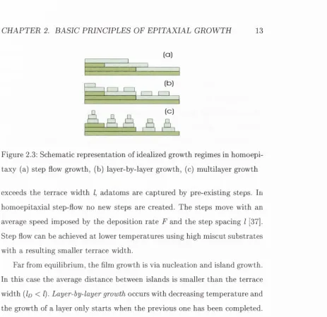
The morphology of a homoepitaxial multilayer film is determined by kinetic mechanisms which are thermally activated processes. Thin films kinetics can involve the transport of atoms within the atomic layer known as intralayer mass transport or the transport of atoms between different atomic layers, process called interlayer mass transport. Depending on the relative rate of the two processes three different growth modes can be distinguished. These are ideally represented in Fig. 2.3.
Step-flow growth was first described in the work of Burton, Cabrera and Frank [36]. Step-flow does not require any interlayer mass transport and it usually produces flat films. It is present in conditions close to equilibrium as it requires rapid intralayer transport to precede nucleation. In these conditions, the diffusion coefficient D and the critical nucleus i are large and according to the nucleation theory (relation (2.11)) the island number density N is small. If the average island separation 1^, given by
CH APTER 2. BA SIC PRINCIPLES OF EP ITA X IA L G RO W T H
13
(a)
I I
(b)
[image:45.540.59.522.67.517.2]A
(c)Figure 2.3: Schematic representation of idealized growth regimes in homoepi
taxy (a) step flow growth, (b) layer-by-layer growth, (c) multilayer growth
exceeds the terrace width /, adatoms are captured by pre-existing steps. In
homoepitaxial step-flow no new steps are created. The steps move with an
average speed imposed by the deposition rate
F
and the step spacing
I
[37].
Step flow can be achieved at lower temperatures using high miscut substrates
with a resulting smaller terrace width.
Far from equilibrium, the film growth is via nucleation and island growth.
In this case the average distance between islands is smaller than the terrace
width
{I
d< I)- Layer-by-layer growth
occurs with decreasing tem perature and
the growth of a layer only starts when the previous one has been completed.
However, a steady interlayer transport must be present. The conditions for
nucleation of the second layer are almost identical to those on the origi
nal substrate. This growth mode requires all atoms deposited on top of the
growing islands to reach the island edge and to jum p onto the lower layer.
C H A P TE R 2. B A SIC PRIN C IPLES OF E P ITA XIA L G RO W TH
14
layer defines the initial lateral length scale. A particular case is the
self-affine growth
[38]. It occurs at sufficiently low temperatures where impinging
atoms remain where landed
{i> <
FJl). This diffusionless growth has a random
appearance, with fluctuation in the film thickness over a large length scale.
The roughness increases during growth but this is not associated with the
selection of a characteristic lateral length scale.
In general, the growth modes are rarely observed in their pure form.
Their particular morphology is usually a mixture of growth mechanisms and
a specific growth mode is present only for a limited thickness range.
2 .4
T h e ste p ed g e barrier
C H A P T E R 2. B A S I C P R IN C IP L E S O F E P IT A X I A L G R O W T H 15
A E
i kD
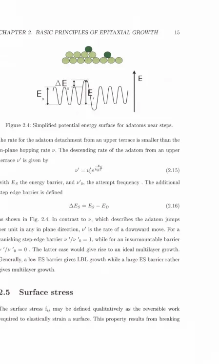
Figure 2.4: Simplified potential energy surface for adatom s near steps.
the rate for the adatom detachm ent from an upper terrace is smaller than the
in-plane hopping rate u. The descending rate of the adatom from an upper terrace i/' is given by
u' = (2.15)
with E s the energy barrier, and u'o, the attem pt frequency . The additional step edge barrier is defined
A E s = E s — Ed (2-16)
as shown in Fig. 2.4. In contrast to u, which describes the adatom jum ps per unit in any in plane direction, u' is the rate o f a downward move. For a vanishing step-edge barrier u '/ u 'o = I, while for an insurmountable barrier ^ ^0 = 0 . The latter case would give rise to an ideal multilayer growth. Generally, a low ES barrier gives LBL growth while a large ES barrier rather
gives multilayer growth.
2.5
Surface stress
The surface stress fjj may be defined qualitatively as the reversible work
[image:47.540.64.513.44.788.2]C H A P T E R 2. B A S I C P R I N CI P LE S OF E P IT A X I A L G R O W T H 16
the high sym m etry environment o f the bulk crystal at its surface. The surface stress is defined as a second rank tensor which relates the change in the total
excess free energy o f the surface 7A and to a change in the surface area by an infinitesim al elastic strain, deij:
Since d (7A) = 7dA + A d7, and dA = ASijdeij (where 6ij is the Kronecker delta), the surface stress can be expressed as:
For surfaces w ith a threefold or higher rotation axis of symmetry, the surface stress can be taken as the scalar f,
This equation shows that the difference between surface stress and surface free energy is equal to the change in surface free energy per unit change in the elastic strain o f the surface. For clean surfaces, surface stress values are of the same order o f m agnitude as the surface free energy but while 7 is always positive f may be positive or negative leading to cases of tensile (f > 0) and compressive (f < 0) stress respectively. For a liquid surface j — f as d j / d e = 0 where 7 is known as surface tension.
2.6
M isfit d islocation s in ep itaxial layers
di j A)
=Afijdeij
(2.17)(2.18)
(2.19)
C H A P T E R 2. B A SIC PRIN C IPLES OF E P IT A X IA L G RO W TH
17
m aterial lattice parameter (a^) and the substrate lattice param eter (a^)
m
=
~
X100
(2.20)
Cig
The lattice mismatch induces a
misfit strain within the film, which forces
the film layers into a m etastable artificial structure. The strain strongly in
fluences diffusion mechanisms and nucleation kinetics, which modifies the
overall growth scenario [41].
Considering the FM growth, the film is homogeneously strained into reg
istry with the substrate in the surface plane. The strain is accommodated by
lattice distortions in the vertical direction in order to maintain the constant
volume of the lattice unit cell. Depending on misfit, whether it is positive or
negative, the distortion will be an expansion or a contraction which defines
the
compressive strain or the
tensile strain respectively. The film stress
a
is
related to the film strain e by the elasticity modulus
B
o = B t = 2G{l + u)
(2.21)
where
G is the shear modulus and
v is Poisson’s ratio. Considering biaxial
strain, the stress is [42]
^ (2^2 2)
The corresponding elastic strain energy per unit area in the film surface plane
is given by [42]
+
(2^23)
where e = m. The lattice distortion normal to the surface plane is given
by [43]
d =
(2.24)
C H AP T ER 2. BASIC PRINCIPLES OF EPITAXIAL G RO WT H 18
per unit length is given by [44]
Es = - (2.25)
47t(1 — l/j To
where b is the dislocation Burger’s vector, R is the is the extent of disloca tion’s strain field and tq is the core dislocation radius, and e the base of the natural logarithm. In the case of a dislocation array in the epilayer, R is the actual epilayer thickness (/i). The elastic energy per unit area {p‘^/2p, where p = h /m is the dislocation spacing) of a two orthogonal square grid of edge dislocations can be then written as
^ Gb"^ , eh , ,
Es = ^ I n — 2.26
27t(1 - v)p ro
W ith the onset of dislocation, the epilayer misfit is partially reduced and con tains a variable term as the residual strain (e) and the misfit accommodated by dislocations (m = e -I- <^). The remaining elastic strain is given by
b
e = m - - 2.27
P
The total energy per unit area of the partially relaxed epilayer is then
E = + (2 . 28)
[ l - v ) 2 7 r ( l - i / ) \ r o )
The model of van der Merwe is based on the requirement that the total energy E has a minimum with respect to the elastic strain e [ dE \ 9e = 0). For a given thickness the minimum energy occurs for a value e o given by
^0 “ Q ---(2.29) M h { \ + v ) \ r o J
The critical thickness (h^) at which it becomes energetically favorable for the first dislocation to be introduced is obtained for e o = ni)
he = T r ^ ( — 1 (2-30)
C H A P TE R 2. BASIC PRINCIPLES OF EPITAXIAL G R O W T H 19
C hapter 3
E xperim ental details
3.1
T he ultrahigh vacuum set up
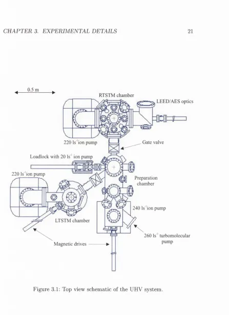
The original UHV system was designed and constructed by Prof. I. V. Shvets,
Dr. A. Quinn and Dr. J. Osing. It consists of three main chambers: the
preparation chamber, the room-tem perature STM (RTSTM) chamber and
the low tem perature STM (LTSTM) chamber. The layout of this system is
shown schematically in Fig. 3.1. A full description of the construction and
operation of the STM and preparation systems is given by Quinn [46].
Each chamber can be valved off from the rest of the system via a series of
UHV gate valves (VAT [47]) and brought to atmospheric pressure for main
tenance without breaking vacuum in the rest of the system. Samples and
STM tips are introduced to the system via a fast-entry loadlock connected
to the preparation chamber by a gate valve. When not in use, this loadlock
is usually maintained in the low 10“ ®
mbar range by a 20 L • s“ ^ differen
tial ion-pump (Perkin-Elmer [48]). Tip and sample transfer throughout the
chamber is facilitated by a series of wobblesticks and magnetically-coupled
linear drives (Vacuum Generators Ltd. [49]) which can access each sample
C H A P T E R 3. EXPERIMENTAL DETAILS 21
0.5 m
RTSTM chamber
r
'V
220 Is 'ion pump
Loadlock with 20 Is ' ion pump
LEED/AES optics
Gate valve
220 Is 'ion pump
Preparation chamber
□
240 Is' ion pump
S
LTSTM chamber
Magnetic dnves
260 Is' turbomolecular pump
[image:53.542.57.504.50.665.2]C H A P T E R 3. E X P E R IM E N T A L D E T A IL S 22
stage. The pressure in each cham ber is m onitored using nude Bayard-A lpert type ionisation gauges (Perkin-Elm er). The entire system is supported on a
stainless steel box-section fram e which can be floated on pneum atic dam pers to isolate the system from building vibrations during STM operation. The box-section is filled w ith gravel to minimise hollow pipe vibrations.
3.2
T h e p rep aration cham ber
T he preparation cham ber was designed by Dr. S. M urphy [88] and m anu factured by C aburn-M D C Ltd. [50]. To achieve UHV the chamber is usually baked for 3 days at 170-180 °C. A custom ised bake-out tent was designed for the preparation cham ber [53]. A base pressure in the low ~ lO^^*’ m bar is obtained in this cham ber after baking out.
A num ber of pum ps are used to achieve UHV conditions in the chamber: the first is a TM U 260 L • s~^ turbom olecular pum p (Pfeiffer Vacuum [51]). This pum p is backed by a 0.7 L • s“ ^ two-stage rotary vane pump. A double- ended 240 L • s“ ^ differential ion-pum p (Physical Electronics [48]) is used to m aintain UHV conditions. A liquid nitrogen cryoshroud is inserted in th e base flange of the ion-pum p which houses a titan iu m sublim ation pum p (TSP). A non-evaporable getter pum p (NEG) from SAES G etters [55] is positioned mid-way along the cham ber. This pum p is particulary effective pum ping out hydrogen.
T he cham ber contains all the facilities for in-situ tip and sample prepa ration: electron-beam and resistive heaters, quartz crystal deposition m on ito r (Inficon [54]), a triple evaporator w ith integral flux m onitor, ion-gun
C H A P T E R 3. E X P E R IM E N TA L D ETAILS
23
contains a cylindrical mirror analyser (CMA) based AES subsystem (Perkin-
Elmer) for sample characterization. A detailed description of the main sample
preparation facilities used for the preparation and analysis of the thin films
and magnetite crystals covered in this thesis is given below.
3.2.1
T h e ion gun
The preparation chamber is fitted with an inert sputter ion source (PSP
vacuum technology [59]), which is used for Ar+ ion etching of STM tips and
for some sputtering experiments. The argon gas is introduced by leak-valve
directly into the gas-cell of the ion-gun, the base pressure in the chamber
rises to 5 x 10“® <
Phase
< 1 X 10“ ^ mbar. An energy from 0.5 to 3 KeV
is applied to the ions for rapid cleaning of samples in UHV. The ions are
created by an oscillating electron discharge inside a chamber at ion energy
(kinetic energy) potential. There are two long life tungsten filaments which
typical filament currents of 2.6 A will run through. Discharge currents used
usually vary from 30-40 mA. The target diameter is taken as 11 mm, which
is the diameter of the circular Ta insert in the resistive heater, into which
the sam ple/tip is mounted for ion-etching. A sam ple/gun working distance
of 100 mm is required for this ion-gun. This insert is isolated from ground
by the surrounding ceramic crucible. The thermocouple spot-welded to this
insert allows the target current to be measured. This is typically of the order
of 8.0 < I < 20.0
fiA
for a 0.5-2 keV beam energy and a chamber pressure
of 1
X10“® mbar.
An estim ate of the amount of material removed from the surface by sput
tering can be calculated knowing the incident ion flux (calculated from the
target current) and the sputter yield Y (the number of target atoms ejected
C H A P T E R 3. E X P E R I M E N T A L DETAILS 24
u = — - — [m.s (3.1)
peN A -n ^ ^
where J is the ion current density (A .m “^), Y the sputter yield (atom s/incid en t ion), M the molar mass of the target matrix (kg.m ol“ ^), p the density (kg.m ”^), e the electron charge (A.s), N,4 is Avogadro’s con
stant (m ol“ ^) and n the number of components yielded per matrix molecule (n = 1 for an elem ental target). For a circular target, this can be re-written as:
A I Y M , ,
V = — , [m.s 1 (3.2)
enD^pNA ^ ^ ^
where I is the target current (A) and D is the sample diameter (m).
3.2.2
T h e resistiv e heater
C H A P T E R 3. EXPERIMENTAL DETAILS 25
Argon ions
i 1
Sam ple Holder
Metal Insert - Alumina
Crucible
T o p
V ie w Filam ent
Support
Evaporation
Side View
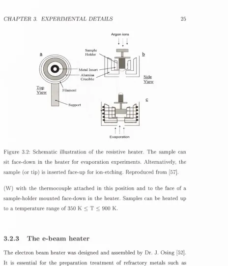
Figure 3.2: Schematic illustration of the resistive heater. The sample can
sit face-down in the heater for evaporation experiments. Alternatively, the
sample (or tip) is inserted face-up for ion-etching. Reproduced from [57].
(W) with the thermocouple attached in this position and to the face of a
sample-holder mounted face-down in the heater. Samples can be heated up
to a temperature range of 350 K < T < 900 K.
3 .2 .3
T h e e-b ea m h eater
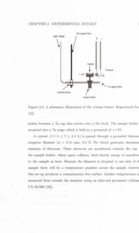
The electron beam heater was designed and assembled by Dr. J. Osing [52].
It is essential for the preparation treatment of refractory metals such as
tungsten and molybdenum. Repeated short flash-annealing of the surface at
very high temperatures (1900 K < Tflash < 2400 K for 10-20 seconds in
UHV) can remove impurities from the surface. A schematic illustration of
[image:57.540.54.518.72.613.2]C H AP T ER 3. EXPERIMENTAL DETAILS 26
Mo support bais high voltage
\
Ta support plate
Figure 3.3: A schematic illustration of the e-beam heater. Reproduced from
[
52
].
holder between a Ta cap that screws onto a Mo body. The sample holder is
mounted into a Ta stage which is held at a potential of +1 kV.
A current (1.5 A < I < 4.5 A) is passed through a grounded thoriated
tungsten filament {(j) = 0.15 mm, 0.6 % Th) which generates thermionic emission of electrons. These electrons are accelerated towards the cap of
the sample holder, where upon collision, their kinetic energy is transferred
to the sample as heat. Because the filament is situated to one side of the
sample there will be a temperature gradient across the sample, however,
this set-up produces a contamination free surface. Surface temperatures are
measured from outside the chamber using an infra-red pyrometer (Altimex
UX-20/600 [58]).
Sample
alum ina beads
[image:58.540.17.469.30.787.2]C H A P T E R 3. EX PE R IM E N TA L D ETAILS
27
3.2.4
The e-beam evaporator
The Cr films were deposited using triple electron beam evaporator from Omi-
cron Gmbh [69]. The principle of operation is the same as th at for e-beam
heater. Electrons originating from a hot (thoriated tungsten) filament are ac
celerated towards a 3N Cr source. A heat-shield is formed around the source
and filament by a tube of Ta foil which sits into grooves cut in the Mo end-
caps. The entire cell fits inside a double-walled water cooled shroud. During
operation, cooling this shroud minimizes outgassing from around the evapo
rator. A new source is outgassed for 6-8 hours before it is suitable to use, it is
also outgassed for further 3-4 hours before each subsequent deposition. Typ
ical values for the filament and emission currents during deposition are 2.3
A and and 25 mA respectively. The Omicron controller maintains a constant
deposition flux by means of a feedback loop. The chamber pressure during
deposition usually rises to not more than the mid-
mbar.
The sample sits upside-down inside the resistive heater as shown in Fig.
3.2 which allows the sample surface to be heated for depositions at elevated
temperatures. This heater stage is also equipped with a water- cooled quartz
crystal balance and deposition monitor (Inficon). The quartz crystal balance
measures the mass of chromium arriving at its surface by measuring the
resonance frequency shift of the quartz crystal sensor. The measured mass
may be converted into film thickness value by the deposition monitor, which
is programmed with values for the density of bcc Cr (7.21
g.crrT^)
and the
exposed sensor (diameter = 8
mm).
However, the thickness value determined
by this method is inacurate as it assumes th a t the Cr deposited on the sensor
surface grows as bcc Cr, which is not the case. Therefore, it is safer to measure
the mass arriving at the sensor surface per second and from this calculate
CHAPTER 3. EXPERIMENTAL DETAILS 28
deposition.
3.3
A uger electron spectroscopy (AES)
The main parts of the Auger spectrometer are the electron gun and the
electrostatic energy analyzer. Auger spectrometer uses a cylindrical mirror
analyzer (CMA, model 10-155A Physical Electronics) with a variable po
tential applied between an inner and outer cylinder and resulting in a signal
which is proportional to the number of detected electrons N at kinetic energy
E. Primary electrons of known energy which are reflected from the sample
surface are used to optimise the signal intensity and calibrate the analyzer.
A beam energy of 3 keV was used for all measurements, the filament
and emission currents were 3.2 A and 1.4 mA respectively, giving a target
current of ~ 8 //A. A SR 850 DSP lock-in amplifier from Stanford Research
Systems [61] was used to output a 0.5 ~Vrms sinusoidal signal of frequency 12
k H z. A lock-in sensitivity of 100 //V was used to detect tlie Auger signal.
The scan speed was always set at 1 eV.s“ \ with scan ranges of 0-750 eV for
magnetite (111) and 0-650 eV for Cr films on Mo(llO).
3.4
Four-grid low energy electron dilfraction
(LEED)
The RVLO 900 four-grid reverse view optics were manufactured by VG Mi
crotech. The optics are mounted on a O.D. 200 mm CF custom elbow which
is tilted at an angle of 30° to the horizontal. The sample sits in the transfer
fork of a magnetic drive, which is grounded by a stainless steel braid to an
C HA P T E R 3. EXPERIMENTAL DETAILS
29
M3
M 2a, M2b
M l screen,
sample
e-gun
“ X
-V +5kV
Figure 3.4: Schematic of four-grid optics operating in LEED mode (c/. refer
ence [62]).
in this drive so th a t its surface faces the electron gun. Scattered electrons are
collected by the grids and screen located behind the gun.
A schematic illustration of the four-grid LEED is shown in Fig. 3.4. The
grid nearest the sample M l is earthed so th a t electrons scattered by the
sample, initially travel in field-free space. A negative potential is applied
to the two centre grids M2a and M2b to suppress inelastically scattered
electrons, while elastically scattered electrons are accelerated towards the
phosphorescent screen by its -1-5 keV potential. The fourth mesh M3 is also
grounded to reduce the field penetration of the suppressing grids by the
screen.
LEED patterns of the metal surfaces were taken at energies between 40
and 200 eV, using an emission current of 0.5 mA. The target current could
[image:61.540.47.522.64.661.2]C H AP T ER 3. EXPE RIME NTA L DETAILS
30
3.5
Scanning tu n n elin g m icroscopy (STM )
The main experimental technique used in this thesis is scanning tunneling mi
croscopy (STM). The theory and principles of STM and spectroscopy (STS)
are given in dedicated texts by Chen and Wiesendanger [63,64]. In STM a
sharp tip is brought very close to a conducting sample. Electrons can travel
across this gap by quantum mechanical tunneling. The fundamental theory
of STM is modelled on the quantum-mechanical description of an electron
with energy E travelling in a ID potential U(z). This electron is described
by a wavefunction ?/’(z), which satisfies the Schrodinger equation:
+ U{z)ip{z) = Exp{z)
(3.3)
where m is the electron mass and
h =
h/2'a (where h is Planck’s constant).
In the classically allowed region where E > U(z), this equation has solutions
of the form:
^{z) = t/>(0)e^**^
k =
(3.4)
where the electron can move in either the positive or negative direction.
In the classically forbidden fiam er region where E < U(z), the Schrodinger
equation has the solution:
j 2 m i U - E)
'il)[z) = -0(0)6
K
=
^
---
(3.5)
The
K
term describes the decay of the electron wavefunction within the bar
rier region. For a finite potential U(z), there is a non-zero probability
P
of
finding the electron at a position z inside the barrier region, which is given
by:
P
oc| V’(O) P
(3.6)
Consequently, if the width of the tunnel barrier is sufficiently narrow, there
C H A P T E R 3. E X P E R IM E N TA L DETAILS
31
vacuum level
sample
eV
0
z
Figure 3.5: Schematic representations of a STM junction under an applied
bias V.
In the tip-vacuum-sample configuration of an STM junction (Fig. 3.5),
the height of the tunnel barrier is determined by the
work function (/)
of
the tip and sample (assumed to be identical for convenience), which is the
minimum energy required to remove an electron from the metal to vacuum.
An electron at the tip or sample surface, with Fermi energy
Ej?
=
—(j)
eV, will
have the greatest opportunity to tunnel through the barrier. In the absence
of an externally applied bias, the electron can tunnel through the barrier in
either direction so th a t there is no net tunnel current. By applying an external
voltage V, electrons in the sample within the energy range
E p —eV < E < Ep
tunnel through the barrier. If
eV
-C 0, then only electron states very near to
the Fermi level are probed. The probability for an electron in the n-th states
to tunnel through a barrier of width W is given by:
y/2m(t)
P
ocj
'i/’n (0 )I e
2 „ - 2kWK
=
h
(3.7)
Taking into account all the possible states in the energy range
Ep — eV <
E < Ep
, the tunnel current is:
Itoc
Y .
I '^(0)
E = E F - e V|2 q- 2kW
[image:63.540.49.518.49.720.2]