Active Metal-Insulator-Metal Plasmonic Devices
Thesis by
Kenneth Alexander Diest
In Partial Fulfillment of the Requirements for the Degree of
Doctor of Philosophy
California Institute of Technology Pasadena, California
2010
c
2010
Kenneth Alexander Diest
This thesis is dedicated to
Carol Ann Diest, Hadley Ann Diest, and Edison Allen Diest
who will have the chance to read this thesis
and
Professor Richard Wood, Mr. Robert Stewart, and Hanna Diest
Acknowledgements
They say that life’s all about the journey, and at the start of this journey I was working as an
engineer at Hewlett-Packard. After deciding I didn’t have enough expertise in any one area to
really drive the field in which I was working, I headed off to graduate school. After five years at
Caltech, it’s definitely about the journey just as much as it is the goal. On paper, you’re a doctor
the day you graduate from the Ph.D. program. In reality, it happens somewhere along the way. As
painful and stressful as the whole process was, it’s definitely made me a better person. Not only
because of the additional mountain of knowledge I’ve digested, but because of the people I’ve met
along the way. Without the help of a great many people, I would not have written this thesis.
The first person I need to thank is my advisor, Harry Atwater. As well as providing all the
labs and funding necessary for me to do my research; he was also a constant source of ideas for the
projects I was involved in. He encouraged me to attend conferences and made it possible to work
with other groups on campus as well as with LETI in France.
My parents deserve as much thanks as anyone. I always tell people that the greatest blessing
that my sister and I had was our parents dedication to our educations’. They gave up a great many
things so that we could have every opportunity to grow academically, athletically, and musically.
The five years here at Caltech weren’t always easy and my close friends were extremely helpful in
getting through all the challenges, academic and otherwise. I couldn’t have gotten through graduate
school without the help of Merrielle Spain, Melissa Archer, Eyal Feigenbaum, Ryan Briggs, Glenn
Garrett, and Krista Langeland.
Young-Bae Park was very helpful as a mentor for my first two years at Caltech. He taught me
about ferroelectrics, ion implantation-induced layer transfer, piezoresponse force microscopy, how
to write a scientific paper, and where to find the best Korean food near Caltech. He was a constant
source of new ideas, and discussions with him lead me to the idea for the silver bonding project.
The difficulty in navigating all the labs and equipment within the Atwater Group is on the
order of developing cold fusion. A number of individuals within the lab were especially helpful
with this task over the years. Luke Sweatlock and Matt Dicken used their wit and sarcasm to
guide me through the first few years of graduate school and introduced me to the art of poker. In
addition, Luke’s work on the plasMOStor project as well as all things plasmonic were key in getting
helping me get up to speed. Luke also provided plenty of ”help” with the more subtle aspects of
on campus to find batteries. Vivian Ferry was especially helpful when analyzing FDTD and the
slit scattering results. Imogen Pryce was helpful with everything in the lab and group during my
final years at Caltech. Stan Burgos was helpful with questions about the FIB and FDTD. Jennifer
Dionne deserves thanks for extracting the TEM sample for the silver bonding paper and her FIB
and simulation work on the plasMOStor project.
I also want to thank everyone else in the Atwater Group including: Koray Aydin, Julie
Biteen-Johnson, Shannon Boettcher, Dennis Callahan, Davis Darvish, Michael Deceglie, Michael Filler,
Carrie Hofmann, Seokmin Jeon, Greg Kimball, Marina Leite, Henri Lezec, Jeremy Munday, Keisuke
Nakayama, April Neidholdt, Deirdre O’Carroll, Domenico Pacifici, Morgan Putnam, Christine
Richardson, Katsu Tanabe, Dan Turner-Evans, and Emily Warmann.
The staff of the Kavli Nanoscience Institute were very helpful. Thanks to Guy Derose, Mary
Sikora, Nils Asplund, Bophan Chhim, Carol Garland, and Melissa Melendes. None of the focused
ion beam work or the silver bonding transmission electron microscope work would have been possible
without them. Also, thanks to the administrators that ran Watson while I was there: Eleonora
Vorobieff, Irene Loera, and Cierina Marks.
I apologize to anyone I’ve forgotten, or anything people have helped me with that I’ve left off
the list.
Finally, I’d like to thank my thesis examination committee: Professors Amnon Yariv, Kaushik
Bhattacharya, Chiara Daraio, and Harry A. Atwater.
Kenneth Diest
September 2009
Abstract
As the field of photonics constantly strives for ever smaller devices, the diffraction limit of light
emerges as a fundamental limitation in this pursuit. A growing number of applications for optical
“systems on a chip” have inspired new ways of circumventing this issue. One such solution to this
problem is active plasmonics. Active plasmonics is an emerging field that enables light compression
into nano-structures based on plasmon resonances at a metal-dielectric interface and active
modula-tion of these plasmons with an applied external field. One area of active plasmonics has focused on
replacing the dielectric layer in these waveguides with an electro-optic material and designing the
resulting structures in such a way that the transmitted light can be modulated. These structures
can be utilized to design a wide range of devices including optical logic gates, modulators, and
filters.
This thesis focuses on replacing the dielectric layer within a metal-insulator-metal plasmonic
waveguide with a range of electrically active materials. By applying an electric field between the
metal layers, we take advantage of the electro-optic effect in lithium niobate, and modulating the
carrier density distribution across the structure in n-type silicon and indium tin oxide.
The first part of this thesis looks at fabricating metal-insulator-metal waveguides with
ion-implantation induced layer transferred lithium niobate. The process is analyzed from a
thermody-namic standpoint and the ion-implantation conditions required for layer transfer are determined.
The possible failure mechanisms that can occur during this process are analyzed from a thin-film
mechanics standpoint, and a metal-bonding method to improve successful layer transfer is proposed
and analyzed. Finally, these devices are shown to naturally filter white light into individual colors
based on the interference of the different optical modes within the dielectric layer. Full-field
elec-tromagnetic simulations show that these devices can preferentially couple to any of the primary
colors and can tune the output color of the device with an applied field.
The second part of this thesis looks at fabricating metal-insulator-metal waveguides with
n-type silicon and indium tin oxide. With the silicon device, by tuning the thicknesses of the layers
used in a metal-oxide semiconductor geometry, the device we call the “plasMOStor” can support
plasmonic modes as well as exactly one photonic mode. With an applied field, this photonic mode
is pushed into cutoff and modulation depths of 11.2 dB are achieved. With the indium tin oxide
device, the doping density within the material is changed and as a result, the plasma frequency
structure is characterized with and without an applied electric field, and measurements show that
when an accumulation layer is formed within the structure, the index of refraction within that layer
Contents
List of Figures xii
List of Tables xv
List of Publications xvi
1 Introduction 1
1.1 Materials and Light . . . 1
1.2 Glass . . . 1
1.3 Optical Properties of Materials . . . 4
1.4 Metals . . . 5
1.4.1 Dispersion and Surface Plasmons . . . 6
1.4.2 Metal Insulator Metal Waveguides . . . 7
1.5 Scope of this Thesis . . . 8
1.5.1 Part I: Ferroelectric Slot Waveguides . . . 9
1.5.2 Part II: Semiconductor Slot Waveguides . . . 11
I Ferroelectric Slot Waveguides 12 2 Ferroelectrics 13 2.1 Introduction . . . 13
2.2 Point Groups and Crystal Symmetry . . . 13
2.2.1 Symmetry . . . 13
2.2.2 Crystal Polarization . . . 14
2.4 Electro-optic Effects . . . 17
2.5 Piezoresponse Force Microscopy . . . 19
2.6 Ion Implantation Induced Layer Transfer . . . 20
3 Ion-Implantation Induced Layer Transfer of Single Crystalline Barium Titanate Thin Films 23 3.1 Introduction . . . 23
3.2 Ferroelectric Materials . . . 23
3.3 Experimental Work . . . 25
3.4 Analysis of the Layer Transfer Process . . . 25
3.4.1 Hydrogen Behavior in Ba-Ti-O-H Phases . . . 27
3.4.2 Cavity Formation and Real Hydrogen Behavior . . . 30
3.4.3 Microstructure of Ion Damaged Barium Titanate . . . 33
3.4.4 Domain Characterization of the Transferred Ferroelectric Layer . . . 35
3.5 Conclusion . . . 37
4 Analysis of Competing Failure Mechanisms in Layer Transferred Thin Films 39 4.1 Introduction . . . 39
4.2 Layer Transfer and Lithium Niobate . . . 40
4.3 Geometry of the System and Stress State of the Film . . . 40
4.4 Stability of Microcracks in the Film . . . 42
4.5 Buckling, Delamination, and Failure of the Film . . . 46
4.5.1 Delamination of a Film with a Semi-Infinite Defect . . . 46
4.5.2 Buckling of the Film . . . 47
4.5.3 Propagation of the Delamination Front Induced by Film Buckling . . . 48
4.5.4 Failure of the Thin Film Induced by Bending . . . 50
4.5.5 Comparisons of the Various Length Scales of the Problem and Criterion for Film Failure . . . 52
4.6 Discussion and Comparison with Experimental Results . . . 54
4.6.1 Effect of the Compressive/Tensile State of the Stress on the Stability of Cracks 55 4.6.2 Effect of a High Compressive Stress on the Film . . . 56
5 Silver Diffusion Bonding and Layer Transfer of Lithium Niobate to Silicon 62
5.1 Introduction . . . 62
5.2 Wafer Bonding Limitations . . . 62
5.3 Experimental Work . . . 64
5.4 Analysis of Silver Diffusion Bonding . . . 65
5.5 Conclusion . . . 69
6 Tunable Color Filters Based on Metal-Insulator-Metal Resonators 71 6.1 Introduction . . . 71
6.2 Color Filtering and Plasmonics . . . 71
6.3 Metal-Insulator-Metal Color Filtering . . . 72
6.3.1 Determining the Experimentally Observed Color . . . 74
6.4 Results from Passive Silicon Nitride Color Filtering . . . 74
6.5 Modeling Active Color Filters . . . 77
6.5.1 Varying the Output Coupling Separation . . . 77
6.5.2 Varying the Output Coupling Depth . . . 80
6.6 Losses . . . 82
6.7 Increasing Slit Transmission . . . 83
6.8 High Density Color Filtering Design . . . 85
6.9 Conclusion . . . 86
II Semiconductor Slot Waveguides 88 7 The plasMOStor: A Metal/Oxide/Si Field Effect Plasmonic Modulator 89 7.1 Introduction . . . 89
7.2 CMOS and the Emergence of Plasmonics . . . 89
7.3 Design and Fabrication of the plasMOStor . . . 90
7.4 Switching Behavior . . . 96
7.5 Time Response Analysis . . . 102
7.6 Conclusion . . . 103
8.2 Carrier Modulation in Active Plasmonics . . . 105
8.3 Fabrication and Characterization . . . 107
8.4 Index Shifting in Indium Tin Oxide . . . 109
8.5 Mode Modulation in Metal/InTiO3/Metal Waveguides . . . 110
8.6 Conclusion . . . 112
9 Conclusions 114 III Appendicies 118 A Dispersion Relations for Metal-Insulator-Metal Waveguides 119 A.1 The General Solution . . . 121
A.2 Boundary Conditions . . . 123
A.2.1 Ex and Dz are continuous: . . . 124
A.2.2 Ey is continuous: . . . 125
A.2.3 Hz,Hy, and Bz are continuous: . . . 125
B Tensor Representation of Crystals 127 B.1 Tensor Notation . . . 127
B.2 Orientation Effects of Crystal Properties . . . 130
C Spectroscopic Ellipsometry 132
D Lithium Niobate Optical Properties 135
List of Figures
1.1 The Lycurgus Cup. . . 3
1.2 Surface Plasmons . . . 8
1.3 The Metal-Insulator-Metal Waveguide . . . 9
1.4 Metal-Insulator-Metal Generalized Schematic. . . 10
2.1 32 Crystal System Symmetries . . . 14
2.2 ABO3 Perovskite Unit Cell . . . 15
2.3 Landau Spontaneous Polarization . . . 18
2.4 Piezoresponse Force Microscopy . . . 19
2.5 Contact Angle Measurements . . . 21
2.6 The Layer Transfer Process . . . 22
3.1 Contact Angle Measurements . . . 26
3.2 Equilibrium concentration of available species in implanted BaTiO3 as a function of temperature and pressure . . . 28
3.3 Equilibrium concentrations in the Ba-Ti-O-H system during cavity formation . . . . 29
3.4 Cracking and blistering during layer transfer . . . 31
3.5 Forward recoil electron spectroscopy of implanted BaTiO3 . . . 32
3.6 Raman spectroscopy of BaTiO3 before, durning, and after layer transfer and post-bond annealing . . . 33
3.7 TEM of layer transfered BaTiO3 . . . 34
3.8 AFM and PFM of bulk and layer transfered BaTiO3 . . . 35
3.9 AFM and PFM of BaTiO3 films using PLD and layer transfer . . . 36
3.10 Hysteresis curves of PLD and layer transfered BaTiO3 . . . 37
4.2 Geometry of a perturbed crack propagating in a film . . . 43
4.3 Debonding with and without buckling . . . 48
4.4 Energy release rate of an interfacial crack . . . 49
4.5 Crack evolution diagrams thick and thin transfered layers . . . 51
4.6 Transverse cracks during layer transfer under no applied stress . . . 55
4.7 Telephone-cord-like cracks in compressively stressed LiNbO3 . . . 56
4.8 A buckled region of LiNbO3 . . . 57
4.9 Crack evolution diagram for the experimentally tested LiNbO3 . . . 59
5.1 TEM sample extraction in the FIB . . . 65
5.2 TEM of Lithium Niobate Sample . . . 66
5.3 Formation of the Silver Bond . . . 67
5.4 Silver Grain Growth . . . 68
5.5 Silver XRD before and after annealing . . . 69
6.1 Lithium Niobate MIM Device Schematic . . . 72
6.2 Lithium niobate membrane fabrication . . . 73
6.3 Lithium niobate membranes before and after FIB . . . 74
6.4 1964 CIE RGB Color Matching Functions . . . 75
6.5 1964 CIE RGB Color Matching Functions . . . 76
6.6 Silicon Nitride MIM Device Dispersion . . . 76
6.7 Lithium Niobate Output Colors with Varying Slit Spacing . . . 78
6.8 Power transmission through LiNbO3 waveguides . . . 79
6.9 Lithium Niobate MIM Dispersion Diagram . . . 80
6.10 Mode Profiles within MIM Waveguides . . . 81
6.11 Trapezoidal Slit Transmission with varying Dimensions . . . 84
6.12 Trapezoid/Rectangle Hybrid Slit Transmission with varying Dimensions . . . 85
6.13 Three-dimensional Implementation of MIM Color Filters . . . 87
7.1 plasmostor Membrane Fabrication . . . 91
7.2 XRD and Raman measurements of Silicon Membrane Strain . . . 92
7.3 plasmostor Device Schematic . . . 93
7.5 plasMOStor Dispersion . . . 95
7.6 plasMOStor Dispersion . . . 96
7.7 plasMOStor FDTD Simulations atλ= 1550 nm . . . 97
7.8 plasMOStor FDTD Simulations atλ= 685 nm . . . 98
7.9 Capacitance-voltage and switching behavior of individual devices. . . 99
7.10 plasMOStor Switching . . . 100
7.11 plasMOStor Circuit Analysis . . . 104
8.1 Plasma Frequency as a Function of Carrier Density . . . 107
8.2 MOS Structure Studied for InTiO3 Ellipsometry . . . 108
8.3 Ellipsometry of InTiO3 Under Applied Field . . . 109
8.4 Calculated Broadband Complex Index of InTiO3 . . . 110
8.5 Accumulation Layer Complex Index in InTiO3 . . . 111
8.6 Optical Modes in a Au/InTiO3/SiO2/Au Waveguide . . . 112
9.1 Summary of Parameters Studied to Affect Color Filter Output Spectrum . . . 115
9.2 Summary of Parameters Studied to Affect plasMOStor Output Spectrum . . . 116
A.1 Coordinates for MIM Dispersion Calculations . . . 119
B.1 Three-Dimensional Piezoresponse Plot for Barium Titanate . . . 131
C.1 Schematic of Spectroscopic Ellipsometry . . . 133
List of Tables
3.1 Possible equilibrium species in the Ba-Ti-O-(H) . . . 28
7.1 5-layer Stack Used in plasMOStor Modeling . . . 96
List of Publications
Portions of this thesis have been drawn from the following publications:
Tunable Color Filters Based on Metal-Insulator-Metal Resonators. K. Diest, J.A. Dionne, M. Spain,
and H.A. Atwater, Nano Letters, 9, 2579 July 2009
Competing failure mechanisms in thin films: application to layer transfer. L. Ponson, K. Diest,
H.A. Atwater, G. Ravichandran, and K. Bhattacharya, Journal of Applied Physics, 105, 073514
April 2009
PlasMOStor: a metal-oxide-Si field effect plasmonic modulator. J.A. Dionne*, K. Diest*, L.A.
Sweatlock, and H.A. Atwater, Nano Letters, 9, 897 January 2009
Silver diffusion bonding and layer transfer of lithium niobate to silicon. K. Diest, M.J. Archer, J.A.
Dionne, Y.B. Park, M.J. Czubakowski, and H.A. Atwater, Applied Physics Letters, 93, 092906
September 2008
Single crystalline BaTiO3 thin films synthesized using ion implantation induced layer transfer. Y.B.
Park, K. Diest, and H.A. Atwater, Journal of Applied Physics 102, 074112 October 2007
Growth and optical property characterization of textured barium titanate thin films for photonic
applications. M.J. Dicken, K. Diest, Y.B. Park, and H.A. Atwater, Journal of Crystal Growth300,
330 March 2007
titanate and lead titanate thin films. J.L. Ruglovsky, J. Li, K. Diest, K. Bhattacharya, and H.A.
Chapter 1
Introduction
1.1
Materials and Light
Light, earth (materials), and their interaction; these topics have been studied for thousands of
years. The materials that make up our world truly are the “Substance of Civilization” [104]. In
many ways, the history of our world has been defined by the materials we have had at our disposal.
Many of the periods in human history have been characterized by the materials that were available:
the stone age, the bronze age, the iron age, the industrial revolution (which came about in no small
part from the development of manufactured steel), and the silicon age. Many periods of human
advancement can be attributed to materials development for military and scientific applications.
In addition, civilizations that had not developed militarily, historically fell victim to civilizations
that had. As Tadahiro Sekimoto, former president of Nippon Electric Corporation, said:
“Those who dominate materials, dominate technology.”
This holds true for the future as well as the past. Recent research on plasmonics has
demon-strated negative refraction at visible frequencies [66]. This advancement could lead to optical
superlenses which may rival the best microscopes in existence today, as well as the possibility of
“cloaking” objects from an outside observer [92]. Finally, work by Roddenberry et al. has looked
at using dilithium crystals to travel faster than the speed of light [7]. Until that time comes, we
must focus on materials currently available to us, and by far, the most prevalent optical material
is glass.
1.2
Glass
In its most basic form, glass is a combination of silicon (the 2nd most abundant material in the earth’s crust) with oxygen (the most abundant material in the earth’s crust). This simple
optical telescopes, and a vast number of other applications. A metastable material, glass is basically
a supercooled liquid frozen in place at room temperature. The fact that it’s flowing, just extremely
slowly, is evident from looking at the wavy windows in an old house or church that are actually
thicker at the bottom than the top.
The first use of glass was not for optical purposes; rather, obsidian (volcanic glass which cools
as it reaches the earth’s surface) was cleaved into pieces and used as weapons and tools in the 7th millennium B.C.E. The first evidence of glass making was around 3000 B.C.E. in an area called the
Canaanite-Phoenician coast near the Mediterranean (just north of present-day Haifa). The sand
from this region contained the right concentrations of lime and silica, so that the traders of this
region needed only to mix in natron (a mix of soda ash, baking soda, salt, and sodium sulfate)
while the melt was placed into a hot fire [104].1
The earliest glasses developed in this manner were opaque rather than transparent due to
scattering from small air bubbles or particles trapped within the glass during formation. Later,
during the 1st millennium B.C.E., hotter kilns were developed and artisans began to introduce
metal oxides into the glass to control the color. By forming the glass either with or without
charcoal present, the glassworkers were able to either reduce or oxidize the copper, respectively,
and as a result, produce glass that was either red or blue, respectively.
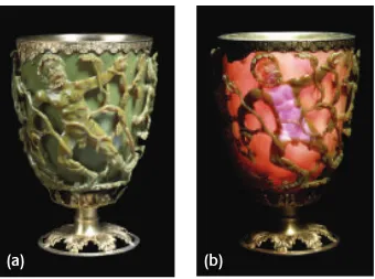
One of the most famous examples of metal being introduced into glass is the Lycurgus Cup.
This glass was produced during the 4th century A.D. during the Roman Empire (Figure 1.1). The cup depicts the death of King Lycurgus in Thrace at the hands of Dionysus. As can be seen from
Figure 1.1, the glass appears red (a) when seen with light transmitted through the cup, and green
(b) when seen with light reflected off the surface of the cup. This remarkable behavior results
from the introduction of colloidal gold and silver into the glass during formation. The resulting
gold-silver nanoparticles within the glass reflect the green portion of the visible spectrum while
transmitting the red portion of the visible spectrum. A theory for this type of scattering from
metal spheres would not be formalized until 1908 by Gustav Mie [72], '2200 years after the cup was made.
It was not until the 13th century that people began developing glass for scientific purposes and the idea of using glass to focus light became a reality. In the 1200s, the Italians invented eyeglasses
1Interestingly enough, around 1400 - 1300 B.C.E. the Phoenicians and Aramaeans of this trade route needed
a method for recording all the financial information from their trades and as a result, developed the alphabetic
The Lycurgus Cup –
A Roman
Nanotechnology
Ian Freestone
1, Nigel Meeks
2,
Margaret Sax
2and Catherine Higgitt
21
Cardiff School of History and Archaeology, Cardiff
University, Cardiff CF10 3EU, Wales UK
2
Department of Conservation, Documentation and
Science, The British Museum, London WC1B 3DG, UK
Introduction
The Lycurgus Cup (fig 1) represents one of the outstanding
achievements of the ancient glass industry. This late Roman
cut glass vessel is extraordinary in several respects, firstly in
the method of fabrication and the exceptional workmanship
involved and secondly in terms of the unusual optical effects
displayed by the glass.
[image:20.612.137.477.72.325.2]The Lycurgus Cup is one of a class of Roman vessels known
as cage cups or diatreta, where the decoration is in openwork
which stands proud from the body of the vessel, to which it is
linked by shanks or bridges Typically these openwork “cages”
comprise a lattice of linked circles, but a small number have
figurative designs, although none of these is as elaborate or
as well preserved as the Lycurgus Cup. Cage cups are generally
dated to the fourth century A.D. and have been found across
the Roman Empire, but the number recovered is small, and
probably only in the region of 50-100 examples are known [1,
2]. They are among the most technically sophisticated glass
objects produced before the modern era.
The openwork decoration of the Lycurgus Cup comprises
a mythological frieze depicting the legend of King Lycurgus
from the sixth book of Homer’s Iliad. The figures, carved in
deep relief, show the triumph of Dionysus over Lycurgus.
However it is not only the cut-work design of the Cup that
shows the high levels of skill involved in its production. The
glass of the cup is dichroic; in direct light it resembles jade
with an opaque greenish-yellow tone, but when light shines
through the glass (transmitted light) it turns to a translucent
ruby colour (Fig 1a and b).
The cup was acquired by the British Museum from Lord
Rothschild in 1958 (with the aid of a contribution from the
National Art Collection Fund) [3]. The mythological scenes on
the cup depict the death of Lycurgus, King of the Edoni in
Thrace at the hands of Dionysus and his followers. A man of
violent temper, Lycurgus attacked Dionysus and one of his
Gold Bulletin 2007 • 40/4
270
Figure 1 (a and b)
The Lycurgus Cup
1958,1202.1 in reflected (a) and transmitted (b)
light. Scene showing Lycurgus being enmeshed by Ambrosia, now
transformed into a vine-shoot. Department of Prehistory and Europe,
The British Museum. Height: 16.5 cm (with modern metal mounts),
diameter: 13.2 cm. © The Trustees of the British Museum
(a)
(b)
Figure 1.1. The Lycurgus cup shown in both reflection (a) and transmission (b). Gold-silver
nanoparticles are responsible for the strong reflection of green light and transmission of red light [1].
which focused the direct and scattered light from objects whose sizes normally spanned millimeters
to kilometers. At the end of the 16th century, Hans Lippershey and Zacharias Jannsen produced two inventions that have changed the world. One, which was also developed by Jacob Metius, was
the refracting telescope. A year later, an improved version was used by Galileo Galilei to focus light
from the stars whose sizes spanned kilometers to billions of light years. Around the same time,
with the help of Sacharias Jansen (Zacharias’ dad), these men invented the microscope. Since then,
this tool and its successors have focused light from millimeters down to nanometers.
Scientists have since been “focused” on exploring and manipulating nature on a smaller and
smaller scale. Unfortunately, in the field of optics, this trend of ever smaller optics eventually
reached a fundamental limit, diffraction. When the smallest dimension of an optical system, such
as a waveguide, reaches 2λn whereλ is the wavelength of the light andn is the refractive index of the waveguiding material, the device is diffraction limited. Below this limit, the waveguide will no
longer be guided through the optical system. One method of getting around this diffraction limit
that has evolved over the past 100 years, but has only taken off in the past 10, has been the field
of plasmonics.
studied the effects of radio waves propagation along the surfaces of conductors in 1899 and 1907,
respectively [106, 128]. As mentioned above, Gustav Mie published work on scattering from metal
spheres in 1908 [72]. In 1957, Ritchie studied electrons at the surface of metallic films using
electron energy loss spectroscopy [99], and in 1968, Ritchie published work on optical interactions
with metallic gratings [100]. In the 1960’s, methods for prisim coupling free-space light into surface
plasmons was reported by Otto [82] as well as Kretschmann and Raether [60]. Since then, there
have been thousands of papers published in the field of surface plasmons including the paper by
Ebbesen et al. in 1998 which described enhanced optical transmission through sub-wavelength
arrays [39]. This discovery was followed by the emerging field of “plasmonics” which is focused on
developing device applications that utilize plasmonic effects.
1.3
Optical Properties of Materials
Any rigorous discussion of the interaction between light and materials begins with Maxwell’s
equa-tions. In the absence of space charge and currents, we have:
∇ ·E~ = 0 (1.1a)
∇ ·B~ = 0 (1.1b)
∇ ×E~ =−1
c ∂ ~B
∂t (1.1c)
∇ ×B~ = 1
cεi(ω) ∂ ~E
∂t (1.1d)
In addition, we have the following constitutive relations for linear, non-magnetic materials:
~
D=0 ~E (1.2a)
~
B=µ0µ ~H (1.2b)
~
P =0χ ~E (1.2c)
where Equation 1.2a relates the dielectric displacement, D~, to the electric field, E~, through the
dielectric constant, ; Equation 1.2b relates the magnetic induction, B~, to the magnetic field, H~,
dielectric function of a material. While this representation of the material’s optical constants is
more explicitly used with Maxwell’s equations, an equivalent form of this property is given by the
complex index of refraction: ˜n =n+iκ. Here, n is the ratio of the speed of light in vacuum to
the speed of light in the material, and κ is the extinction coefficient of light within the material.
This representation is more directly related to the experimental observation of light interacting
with matter. Depending on the situation, the two equivalent forms will be used in this thesis, and
related by:
1 =n2−κ2 (1.3a)
2 = 2nκ (1.3b)
n=
r 1
2 + 1 2
q
21+22 (1.3c)
κ= 2
2n (1.3d)
and κ is related to the absorption coefficient “α” of light propagating through a material by:
α= 2κωc .
1.4
Metals
Traditionally, when materials are considered to design optical waveguides, metals are not the first
thing that come to mind. Metals can be thought of as a sea of free electrons oscillating around a
lattice of fixed ion cores. These electrons are free to move throughout the metal and respond when
the metal experiences an applied external field. When exposed to an optical field at microwave and
far-infrared frequencies, many metals behave like a perfect electrical conductor. The electrons are
able to respond to the external stimulus with the same frequency as the applied field. This gives rise
to the high reflectivities and negligible electromagnetic field penetration traditionally associated
with metals. As the frequency of the field increases, so does the response of the electrons. For
noble metals like gold, silver, and copper, this process continues up to visible frequencies. In this
regime, metals reach a point of maximum oscillation where the driving field strongly couples into
the longitudinal oscillations of the bulk electrons within the metal. This is known as the plasma
ωp =
r
4πne2
m∗ (1.4)
where “n” is the density of electrons within the metal and “m∗” is the effective mass of the electrons.
Above this frequency, the metal behaves as a dielectric and experiences significant electromagnetic
field penetration into the metal.
Separate from these “bulk plasmons” are a type of electron wave within metals known as a
surface plasmon polaritons (SPPs). A SPP is a collective electron density oscillation at the interface
between a metal and a dielectric; these SPPs will be the focus of this thesis. Hereafter, when the
phrase “plasmon” is used, surface plasmon polaritons will be the intended meaning.
1.4.1 Dispersion and Surface Plasmons
Even though and ˜n are referred to as constants, in many situations, these properties can vary
significantly depending on the configurations in which they are used as well as the frequency of the
light involved. This property of materials is known as dispersion.
To calculate the dispersion of these structures, we start with an incident electromagnetic wave
of the form:
~
E(x, y, z)∼E0ei(kxx−kz|z|−ωt) (1.5)
whose electric field has a perpendicular component to the waveguide (transverse-magnetic
polar-ization). Here the components of the electric field within the metal are given by:
Exmetal = E0ei(kxx−kz1|z|−ωt) (1.6a)
Eymetal = 0 (1.6b)
Ezmetal = E0
− kx kz1
ei(kxx−kz1|z|−ωt) (1.6c)
and the components of the electric field within the dielectric are given by:
Exdielectric = E0ei(kxx−kz2|z|−ωt) (1.7a)
Eydielectric = 0 (1.7b)
Ezdielectric = E0
− 1kx 2kz1
and2 represent the wavevector and dielectric constant within the dielectric layer. For both sets of
equations,kxrepresents the component of the wave vector in the direction of propagation along the
metal-dielectric interface. Similarly,kz represents the component of the wave vector perpendicular
to the metal-dielectric interface and from this, we obtain the decay length of the electro-magnetic
field into the layers:
ˆ
z= 1
|kz| (1.8)
By requiring continuity of the E~ and B~ fields at the interface between the two layers, we obtain
the dispersion relation for a single metal-dielectric interface [71, 108]:
kx = ω
cnspp (1.9a)
kz21,2 = 1,2
ω c
2
−kx2 (1.9b)
where the effective surface plasmon index is given by:
nspp=
r 12
1+2
(1.10)
1.4.2 Metal Insulator Metal Waveguides
One of the benefits of coupling light from free space into surface plasmons, is that you can
signifi-cantly reduce the wavelength of the light. Taking this design one step further, by placing a second
metal layer above the dielectric layer as well as below, one can fabricate a metal-insulator-metal
(MIM) waveguide. These structures allow extremely high modal confinement of light.
Dispersion calculations for the MIM geometry are reported in Appendix A and the results are
reported here. For transverse-magnetic polarized light, the dispersion relations for MIM waveguides
are given by:
2kz1+1kz2
coth(kz1d/2)
tanh(kz1d/2)
= 0 (1.11)
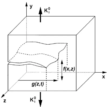
where d represents the thickness of the dielectric layer. A schematic of such a structure and a
representative plot of the dispersion relation is shown in Figure1.3. Seen in the dispersion diagram
are the different plasmonic and photonic modes that would be supported within this structure over
the visible spectrum as a function of the real part of kx. As a reference, the light line for this
metal dielectric
metal
metal
dielectric
Figure 1.2. The figure on the left shows the electric field lines of a surface plasmon at a
metal-dielectric interface. The figure on the right shows the same schematic for a metal-insulator-metal
waveguide.
also labeled. This plot shows the existence of the plasmonic mode as well as one photonic mode
within the structure. Here the plasmonic mode lies to the right of the light line because of the
fact that this mode has a higher momentum than a free-space wave that would couple into it. In
contrast, the photonic mode, whose momentum is strictly less than a free-space wave to which it
would couple, lies to the left of the light line.
The phase and group velocities for these optical modes are defined by:
vp = ω
k (1.12a)
vg= ∂ω
∂k (1.12b)
We can see that near the plasmon resonance in Figure 1.3, vg → 0, and this “slow wave” is characteristic of surface plasmons.
1.5
Scope of this Thesis
As the title suggests, the scope of this thesis is the design and fabrication of active MIM waveguides
SP ! P
!
light line
Metal
Metal
Active Material
Figure 1.3. The figure on the left shows a generalized schematic of the semi-infinite
metal-insulator-metal waveguide. The plot on the right shows a typical dispersion diagram for this type of structure.
Both the plasma and surface plasmon resonances can be tuned over a wide range of the
electro-magnetic spectrum by changing the dimensions of and materials that make up the layers within
the waveguide.
tuned across the visible and infrared portions of the electromagnetic spectrum.
By changing each of the materials in the three layer stack (Figure1.4), as well as their relative
thicknesses, the dispersion properties of the device as well as the resonance and filtering properties
can be tuned over a wide range of the electromagnetic spectrum. In addition, by changing the
dimensions of the in-coupling and out-coupling structures, as well as the distance between them,
we can selectively access a large range of the different waveguide mode profiles that are present
within the structure.
To this end, there are two main sections of the thesis. Each focuses on active MIM waveguides
that utilize a different physical mechanism to induce a change in the region that supports the various
optical modes. The first section looks at the utilizing electro-optic effect in lithium niobate to create
tunable color filters, and the second section looks at modulating the carrier density distribution
across the structure in n-type silicon and indium tin oxide to change the mode profiles within the
waveguide.
1.5.1 Part I: Ferroelectric Slot Waveguides
Part I of this thesis deals with using ferroelectric materials as the active layer between the two
metal cladding layers of the waveguide. The idea is to take advantage of the electro-optic effect
ap-!
Figure 1.4. The schematic on the right shows a typical device that was fabricated using the basic
metal-insulator-metal geometry.
plied electric field. In addition, all the ferroelectric layers used in this thesis were single crystal
and obtained using ion-implantation induced layer transfer. This process has many benefits over
conventional thin-film growth techniques and will be discussed in detail in Chapters 2,3, and 4.
Chapter 2 is an overview of ferroelectric materials and the specific materials properties that
enable them to perform the electro-optic switching discussed above. The chapter finishes with an
overview of ion implantation induced layer transfer which is the method by which the thin film,
single crystal ferroelectric layer are produced in this thesis. In Chapter3, the ion-implantation
in-duced layer transfer process is analyzed from a thermodynamic standpoint and the ion-implantation
conditions required for layer transfer are determined. Assuming the sample has been properly
ion-implanted, Chapter4analyzes the possible failure mechanisms that can occur in the layer transfered
thin-film from the standpoint of thermal expansion-induced stress. The chapter then goes on to
determine the necessary requirements for thin-film and substrate to ensure a coherent layer is
transferred. This analysis is then done for the case of lithium niobate transferred onto a silicon
substrate.
One of the largest difficulties in successful layer transfer is producing a strong, robust bond
intro-the layer transfer process, and during intro-the course of intro-the bonding/layer transfer step, Chapter 5
shows that diffusion bonding causes the two silver layers to become one, continuous layer. The last
chapter in Part I, Chapter 6, looks at passive and active MIM waveguides with silicon nitride and
lithium niobate in the optical channel. These devices are shown to naturally filter white light into
individual colors based on the interference of the different optical modes within the dielectric layer.
Full-field electromagnetic simulations show that these devices can preferentially couple to any of
the primary colors and can tune the output color of the device with an applied field.
1.5.2 Part II: Semiconductor Slot Waveguides
Part II of this thesis deals with using two semiconductor materials (n-type silicon and indium tin
oxide) as the active layer between the two metal cladding layers of the waveguide. Here the idea
is to apply an electric field across the semiconductor layers and modulate the carrier distribution
within the waveguide.
Chapter 7 examines a new type of plasmonic/photonic waveguide whose thickness is carefully
chosen to support one plasmonic mode and exactly one photonic mode very close to cut-off. Through
an extensive experimental analysis and full-field electromagnetic simulations, the device is show to
behave like an MOS capacitor and with an applied field, push the photonic mode into cutoff.
Chapter 8 looks at changing the doping density within transparent conducting oxides (like
indium tin oxide) to shift the plasma frequency into the near-infrared and visible wavelengths. The
material is incorporated into an MOS structure similar to that in Chapter7and through extensive
characterization using spectroscopic ellipsometry (AppendixC), the thin film stack is characterized
with and without an applied electric field. The measurements show that when an accumulation
layer is formed within the structure, the index of refraction within that layer is significantly changed
Part I
Chapter 2
Ferroelectrics
2.1
Introduction
The first part of this thesis is focused on producing an active MIM waveguide with a ferroelectric
layer as the active material. Henceforth, the analysis of ferroelectrics will be done with two materials
which acccurately represent the field, barium titanate (BaTiO3) and lithium niobate (LiNbO3). In
this chapter, we will introduce ferroelectrics and motivate why these materials present a unique
opportunity for use in active plasmonic devices. These materials exhibit a wide range of properties
including piezoelectricity, ferroelectricity, pyroelectricity, and electro-optic effects. The intensity of
these effects within the materials is directly related to the quality of the crystal in question. As a
result, ion implantation induced layer transfer is introduced at the conclusion of this chapter as a
method of producing single crystal thin film ferroelectrics.
2.2
Point Groups and Crystal Symmetry
2.2.1 Symmetry
All crystalline materials can be represented by a crystal lattice and a basis. The lattice represents
the three-dimensional periodic array of points in space. These points form individual “unit cells”
which represent the smallest repeat unit of the lattice. The basis represents the atom or atoms
which lie on each point within the lattice. These crystals can be organized by their symmetry
operations and divided into 32 distinct “point groups”. Of these 32 groups, 11 have a well defined
center of symmetry and are defined as centrosymmetric. Out of the remaining 21 groups, 20 are
piezoelectric [the (432) point group being the only exception]. Out of the 20 piezoelectric point
groups, 10 have a unique polar axis and are referred to as ferroelectric. Below a critical transition
temperature, the Curie temperature (Tc), ferroelectric materials exhibit a spontaneous polarization
Figure 2.1, and the piezoelectric point groups are shown in the boxed, grey region.
Figure 2.1. Shown here are the 32 crystal point groups. The piezoelectric groups are shown in the
boxed, grey region.
2.2.2 Crystal Polarization
The two ferroelectrics that will be studied throughout this thesis are barium titanate (BaTiO3) and
lithium niobate (LiNbO3). BaTiO3 is one of the most well studied and widely used ferroelectrics.
It belongs to a category of materials called ABO3 perovskites. Above Tc, these materials have a
cubic unit cell and below Tc, they have a tetragonal unit cell, Figure 2.2. In the cubic state, the
A atom resides in the center of the unit cell, the B atoms reside on the 8 corners, and the oxygen
atoms lie in the 6 face-centered positions. From a physical standpoint, when cubic BaTiO3 is cooled
below Tc, there is a contraction along the~a-axis and a corresponding elongation along the~c-axis.
As a result, above Tc, the Ba atom sits in the center of the cubic unit cell and is surrounded by
the 4 oxygen atoms in the central plane of the unit cell. Upon cooling below Tc, the contraction in
the~a-axis results in the oxygen atoms moving towards the center of the unit cell, and this forces
the Ba atom to move either above or below the central plane of oxygen atoms, Figure 2.2. This
produces the spontaneous polarization that is associated with ferroelectrics. When the crystal is
result, generate a net electric field. This is the direct piezoelectric effect. The converse of this is
also true. Under an applied electric field, the unit cell dipoles will realign themselves with the field
and change the crystal dimensions. This is known as the converse piezoelectric effect.
T<T
cA
B
a
c
Figure 2.2. The ABO3 perovskite unit cell is shown above (left) and below (right) the Curie
temperature. The A atom is shown in the center, the B atoms are shown on 8 corner sites, and the
oxygen atoms are shown on the face-centered sites.
From an energetics standpoint, Uchino gives the energy of the spontaneous dipole for N atoms
per unit volume as [116]:
Edipole =− N αγ2
920 ~
P2 (2.1)
whereαis the ionic polarizability of the ion,γis the Lorentz factor,0is permittivity of vacuum, and
P is the surrounding polarization. In addition, the elastic energy associated with ion displacement from its equilibrium position,~u, is given by:
Eelastic=N
k
2
~ u2+
k0 2 ~ u4 (2.2)
where k and k’ represent the two spring constants associated with the energy between ions within
a unit cell and between different unit cells, respectively. By assumingP =N q~u, where q is electric charge, we arrive at:
Etotal=Edipole+Eelastic=
k
2N q2
−
N αγ2
92 0
~
P2+
k0
4N3q4
~
This says that if the elastic energy within the crystal is greater than the dipole-dipole
interac-tions, then there is no spontaneous polarization, T>Tc. If the converse is true, then there will be
a spontaneous polarization, T<Tc.
2.3
Landau-Ginsburg Theory of Ferroelectrics
One analytic method of formalizing the second-order phase transition that occurs upon cooling a
ferroelectric below its Curie temperature is to use the Landau Theory of phase transitions. This
theory, which was developed by the Nobel Prize winning physicist Lev Landau, represents the free
energy of a crystal as a phenomenological expression based on the order parameter, Ψ, of the total
polarization. The generalized expression for the Landau free energy of the system, F, is given by [112]:
F =F0+
1 2αΨ
2+1
4βΨ
4+1
2δ
~
∇Ψ
2
−E~Ψ (2.4)
Here,α and β are temperature dependent coefficients, andδ represents a restoring force which
limits the minimum size of ferroelectric domains. This representation, which neglects terms higher
than fourth order, and includes a term for polarization gradients, 12δ
~
∇Ψ
2
, as well as an applied
electric field,−E~Ψ. Due to the fact that the energy must be invariant under polarization reversal, the coefficients of all the odd powers of Ψ are zero.
For the case of ferroelectrics, the order parameter, Ψ, represents the polarization, P, of the unit cell. Landau theory assumes that below the critical temperature, Tc, a spontaneous polarization
will occur and that the components ofP vary continuously across Tc. For the case of BaTiO3, the
change from a cubic to tetragonal unit cell will result in a spontaneous polarization and can be
written as [56]:
F =F0+12 αzPz2+
P2
x+Py2
αxy
+14
β1Pz4+β2
P2
x+Py2 2
+β3
P2
x− Py2 2
+β4
P2
xPy2
+β5Pz2
P2
x +Py2
+12δ
~
∇Ψ
2
−E~Ψ
(2.5)
case, the Landau free energy of the crystal is given by:
F =F0+1 2αP
2
z +
1 4β1P
4
z (2.6)
and the equilibrium polarization of the crystal below the critical temperature is found by:
∂F
∂P = 0 =αP+βP
3 =P α+βP2
(2.7)
which has the solutions:
P0= 0,±
r
−α
β (2.8)
Here we letα=α0(T−Tc) whereα0 = C0. This gives the final form of the spontaneous polarization
as:
P0= 0,±
s
α0(Tc−T)
β (2.9)
From this we can see that above Tc, when the material is paraelectric, there are no real solutions
forP, and below Tc there are two minima which correspond to the two-fold degeneracy inP. For
the case of the tetragonal unit cell of BaTiO3, this corresponds to the±Pz polarization. Also, for
the fourth order expansion, we require that β >0 to ensure real solutions to P for T< Tc. We
also note here thatP ∼ |T−Tc|β, and as a result, the critical exponent β = 12.
A plot of this is shown in Figure2.3. Here,±Pzcan be seen below the x-axis and no spontaneous
polarization can be seen in the curve representing T>Tc. Additionally, ∆ =αΨ2 is shown below
the x-axis which represents the energy penalty for wide domain walls within the ferroelectric.
Although it is beyond the scope of this thesis, at Tcthis formalism for ferroelectrics can be used
to analyze: the absence of any latent heat; a discontinuity in the specific heat; and a divergence in
the susceptibility [112].
2.4
Electro-optic Effects
The response of any crystal to an external field will depend strongly on the frequency of that field.
With visible light, the frequency is ∼ 430 - 750 THz and as a result, only the electrons within a solid can respond. For electro-optic materials, the application of an external electric field will
induce a displacement of the ion cores within the material. This results in a change in the electron
Free Energy T > Tc
T = Tc
T < Tc
Polarization
Ps Ps
!
Figure 2.3. Landau Free Energy of the crystal as a function of polarization at three temperatures:
T > Tc which exhibits no spontaneous polarization, T = Tc, and T < Tc which has a two-fold
solution.
refraction. For the case of an electric field applied in the ˆzdirection, the redistribution of the ions
within the lattice would produce an elongation in the ˆzdirection and a corresponding contraction
in the ˆxand ˆydirections. As a result, the electron density (and index or refraction) would decrease
in the ˆz direction and would increase in the ˆx and ˆy directions.
As discussed in AppendixB, we know that the index within a material is a second-rank tensor
which is given by [116]:
1
n2ij(E) − 1
n2ij(0) =
X k
rijkEk+ X
kl
RijklEkEl (2.10)
where nij(E) and nij(0) are the indicies of refraction with and without an applied electric field,
respectively. rijk is the Pockels coefficient which represents the linear electro-optic effect, andRijkl
is the Kerr coefficient which represents the quadratic electro-optic effect.
As an example, the ABO3 perovskites discussed in Section2.2.2(Figure2.1) show that in their
coefficients for this crystal structure are given by [116]:
R11 R12 R12 0 0 0
R12 R11 R12 0 0 0
R12 R12 R11 0 0 0
0 0 0 R44 0 0
0 0 0 0 R44 0
0 0 0 0 0 R44
(2.11)
2.5
Piezoresponse Force Microscopy
PFM Signal Topography Lock-in Amplifier Feed-back
Figure 2.4. A schematic of a typical PFM setup is shown. Both topography (a) and piezoresponse
(b) as a function of position on the sample are shown.
One method of investigating the behavior of piezoelectrics that will be utilized in Chapter 3 is
Piezoresponse Force Microscopy (PFM). This technique utilizes a standard atomic force microscope
(AFM) with a conductive scanning tip. The tip is rastered across the sample surface in a series
of line scans which are compiled to produce a topological image of the surface of the sample. At
the same time, a lock-in amplifier is used to apply a DC offset to the tip as well as an AC voltage
(traditionally from 1 - 5 kHz). The applied electric fields cause the piezoelectric material to expand
and contract with the AC voltage and this time-dependent response (whose frequency is that of
Figure 2.4. This is necessary because the piezoresponse signal from the sample is usually near the
lower detection limit of the AFM and as a result, the topography will dominate the output signal.
This is especially true with rough samples which might also have surface oscillation frequencies
which are similar to those of the piezoresponse!
In general, the piezoresponse from the sample is given by:
∆z=−d∗V (2.12)
where d∗ is the piezoelectric coefficient of the material and is >0 for positive domains, ∆z is the
change in height of the sample from the converse piezoelectric effect, and V is the applied voltage.
Including the AC voltage gives:
V =VDC+VACsin(ωt) (2.13)
∆z=d∗33VACsin(ωt+ Φ)
Φ =π forPz >0
Φ = 0 forPz<0
(2.14a)
wherePz >0 indicates that there is a spontaneous positive polarization at the crystal/tip interface,
ω is the drive frequency of the AC voltage, and d∗33 is the constrained out-of-plane piezoelectric coefficient. This value is less that d33 for an individual unit cell because of the fact that it is
constrained by the film around it. The two constants are related by the compliance of the film
“sij” and the shear components of the piezoresponse:
d∗33=d33−
2d31s12
s11+s12
(2.15)
2.6
Ion Implantation Induced Layer Transfer
To fabricate single crystals of the ferroelectrics studied in this thesis, we utilize a technique known
as ion implantation induced layer transfer (or layer transfer for short). The process consists of four
main steps. The first, which will be discussed in Chapter 3, is ion implantation. This step consists
two ions are co-implanted, the energies of implantations should be tuned so that the peaks of the
implantation distributions overlap, and these calculations are done using Stopping and Range of
Ions in Matter (SRIM) software [6].
Upon implantation of the single crystal sample, the surfaces of both the implanted sample
as well as the substrate to which it will be bonded are cleaned and “activated” using a plasma
treatment process. The effectiveness of the plasma activation can be determined using contact
angle measurements of the “as treated” surface with a microsyringe imaging system, Figure 2.5.
Figure 2.5. Typical solid-liquid-gas contact angle schematic used in determining the effectiveness
of plasma treatment before wafer bonding.
After surface treatment of the implanted sample and substrate are complete, the two surfaces
are brought in contact under high temperature and pressure. At high temperature, the implanted
species preferentially diffuse through the implanted crystal along the plane of implantation. This
process induces the formation of gas voids. Provided the crystal is under an acceptable amount of
compressive stress during this process (Chapter 4), the edges of these voids grow along the plane
of implantation, join with other voids, and eventually cleave off a thin film single crystal layer of
the implanted material. A schematic of this process is shown in Figure2.6.
Optimizing each of the different steps in Figure 2.6 is non-trivial and Chapters 2, 3, and 4
will discuss research that was done to produce a coherent, layer transferred film. As difficult
3.! Bonding and layer splitting. Blistering occurs at implantation depth while a covalent bond is formed at the bonding interface.
1.! Hydrogen and (Helium or Boron) implantation to desired depth.
2.! Planarization and plasma activation of the surfaces.
H+ H+ H+
H+
Pressure Temperature
4.! Wafer bonded heterostructure.
Figure 2.6. A schematic process flow of the layer transfer process.
techniques. Fabrication methods fall into two broad categories, bottom up and top down. Bottom
up fabrication involves the deposition of successive layers. Using lithography and etching steps
after each deposition, your structure is fabricated from the “bottom up”. This method is extremely
flexible and allows the integration of a wide variety of materials. The drawback to this technique is
that the films will either be amorphous or polycrystalline. On the other hand, top down processing
uses various etch steps to drill into a substrate and fabricate your structure from the “top down”.
Provided you start with a single crystal substrate, this method has the benefit of producing single
crystal structures; however, this technique is not nearly as flexible in terms of integrating different
materials and structures. Ideally, ion implantation induced layer transfer would combine the best
Chapter 3
Ion-Implantation Induced Layer Transfer of Single
Crystalline Barium Titanate Thin Films
3.1
Introduction
In this chapter, we examine the optimization of the ion implantation process by studying the
layer transfer of barium titanate thin films onto silicon-based substrates. Hydrogen and helium
ions were co-implanted to facilitate ion-implantation-induced layer transfer of films from barium
titanate single crystals. From thermodynamic equilibrium calculations, we suggest that the
domi-nant species during cavity nucleation and growth are H2,H+,H2O,Ba2+ and Ba-OH, and that the
addition of hydrogen to the Ba-Ti-O system can effectively suppress volatile oxide formation
dur-ing layer transfer and subsequent annealdur-ing. After ion implantation, barium titanate layers contain
microstructural defects and hydrogen precipitates in the lattice, but after layer transfer, the single
crystal is found to be stoichiometric. Using direct wafer bonding and layer splitting, single
crys-tal barium titanate thin films were transferred onto amorphous silicon nitride and Pt substrates.
Micro-Raman spectroscopy indicated that the density of defects generated by ion implantation in
barium titanate can be significantly reduced during post-transfer annealing, returning the
trans-ferred layer to its single crystal state. Characterization using piezoresponse force microscopy shows
that the layer-transferred thin films are ferroelectric, with domain structures and piezoresponse
characteristics similar to that of bulk crystals. 1
3.2
Ferroelectric Materials
Ferroelectric materials have attracted increased attention as device materials in recent years because
of their potential applications in microelectronics and integrated optics [105]. Furthermore, these
1
materials are attractive for microelectromechanical systems (MEMS) applications due to large
displacement and high output force during actuation [93].
Many different methods have been studied to obtain high quality, thin film ferroelectric layers
[125]. The growth of epitaxial thin films at relatively high temperatures (> 700◦C) has been
reported using metal organic chemical vapor deposition, molecular beam epitaxy, atomic layer
deposition, pulsed laser deposition, chemical solution deposition, and sol-gel processes. Integration
of most of these technologies with conventional silicon-based device applications has proven difficult
because of the high growth temperatures required and the need for an epitaxial template. Due to the
complex set of elastic and electric boundary conditions at each grain, the grains in pressed ceramics
and polycrystalline films are usually composed of multiple domains. If the spontaneous polarization
within each domain is random, or distributed in such a way as to lead to zero net polarization, the
pyroelectric and piezoelectric effects of individual domains will partially or significantly compensate
each other. Additionally, for photonic devices, grain boundaries and domain boundaries can be
sources of light scattering and absorption.
Recently, progress on integration of single crystal ferroelectrics has been made by fabrication
of single crystal thin film layers. Light elements such as hydrogen and helium are implanted into
a wafer at a specified projected range, and a film of equivalent thickness is exfoliated [22, 114].
Recently, successful layer transfer of semiconductors and ferroelectric materials has been reported
[15, 54, 65, 74, 115, 127]. In the work reported here, layer transfer relies on direct wafer bonding
and gas pressure-induced layer exfoliation. This is similar to that used to fabricate
silicon-on-insulator structures, and enables much thinner films to be fabricated. We discuss hydrogen release
and the resulting cavity growth mechanisms for the layer splitting of barium titanate (BaTiO3),
and the role of hydrogen during post-thermal annealing. Together with the thermodynamics and
kinetics of cavity nucleation, growth, and blistering, these results provide an explanation of the
layer exfoliation process. In this study, H+ and He+ were implanted in single crystal BaTiO3 and
subsequently bonded to silicon nitride Si3N4/Si and Pt/Si receptor substrates, which are typical
structures for ferroelectric memory and MEMS devices. Pt is typically used as a bottom electrode
3.3
Experimental Work
Protons were implanted into single-crystal BaTiO3 with energy between 20 and 80 keV with a
dose of 5×10¹⁶ −1 ×1017 cm−2, followed by 30 - 115 keV He+ implantation with a dose of 1×1017 cm−2. All implantations were performed at room temperature. The donor and receptor substrates (sputtered Pt on Si and low-pressure chemical vapor deposition Si3N4on Si) were cleaned
with methanol, acetone, and deionized water. The donor and receptor substrates were brought in
contact at room temperature. Heating during the initial bonding step causes micro-cracks to form
and cavities to nucleate, coalesce, and blister in the implanted region. Isochronal annealing of the
bonded donor material was performed between 300 and 500◦C after initial bond formation, causing
a layer whose thickness is equal to the implanted depth to be transferred to the receptor substrate.
The thermodynamic equilibrium composition at the annealing temperature (300 - 700◦C) was
calculated using the SOLGASMIX-PV code in Chemsage [5], minimizing the total Gibbs free energy
of the system with data from the Joint-Army-Navy-Air Force (JANAF) thermochemical table [40].
Calculations were performed for both Ba-Ti-O and Ba-Ti-O-H systems with the compound
condi-tions of 1:1:3 and 1:1:3:0.1-10, respectively, corresponding to stoichiometic single crystal BaTiO3
with and without the addition of hydrogen.
Blistering was observed by polarized optical microscopy, scanning electron microscopy and
atomic force microscopy. Atomic force microscopy was also used to characterize transferred film
thickness and surface roughness. Micro-Raman spectroscopy, Rutherford backscattering
spec-troscopy, forward recoil elastic specspec-troscopy, energy dispersive x-ray specspec-troscopy, and transmission
electron microscopy analyses were performed to assess the microstructural evaluation of the bulk
crystal and transferred layer. Ferroelectric domain imaging and microscopic hysteresis loop
mea-surements were obtained using piezoresponse force microscopy.
3.4
Analysis of the Layer Transfer Process
The key factors required to achieve covalent bonding between donor and receptor substrates are high
surface flatness, low surface roughness, surface cleanliness, and chemical reactivity. Initial bonding
of bulk, unimplanted BaTiO3crystals was successful since the donor and receptor substrates can be
prepared according to these conditions. Bulk (100) BaTiO3 has a typical lamellar domain pattern
with tetragonal 90◦ a-axis and c-axis domains with sizes ranging from 5 to 400 nm, with a
the surface of the BaTiO3 sample is corrugated with a characteristic angle between domains given
by: θ = 90◦ −2arctan(a/c) where a and c refer to lattice constants of the [100] and [001] axes respectively. The peak-to-valley height of this surface corrugation was found to be in the range
of 2 - 100 nm, depending on the domain size. The RMS roughness of the BaTiO3 donor wafer
slightly increased after ion implantation to 2.4 nm. Using a Monte Carlo simulation method for
calculation of ion implantation and collision cascade characteristics [6], the ion projected range was
determined to be∼430 nm [6]. The Pt coating thickness was 180 nm and the Si3N4 thickness was
50 nm, yielding a receptor substrate RMS roughness of 0.7 nm for Si3N4 coated Si substrates and
3.6 nm for Pt coated Si substrates. After room temperature bonding, no interference fringes were
observed, indicating a distinct lack of surface particles or other contamination.
Figure 3.1. Typical solid-liquid-gas contact angle schematic.
The surface energy of the BaTiO3 single crystals surfaces following H+ implantation was
ob-tained by contact angle measurements using water and di-iodomethane droplets with a constant
volume droplet of 20 dm3using a double laser-beam goniometer. At room temperature, the surface energy is 61.1 mJ/m2 and for the temperature-dependent surface energy, we used the phenomeno-logical equation,γ(T) = 6.11×10⁻²+ 3.82×10⁻⁵T assuming ,γ(T) =γ0(1 +T /T0), where T0 is
3.4.1 Hydrogen Behavior in Ba-Ti-O-H Phases
After ion implantation, the bulk BaTiO3 lattice is filled with hydrogen. This hydrogen passivates
the dangling bonds and defects generated by atomic displacements. In order to describe the behavior
of hydrogen in solid materials, Sieverts law can be applied. Here: c0 = sp1e/2 where pressure, pe,
is related to fugacity, fe, and the hydrogen concentration,c0,in the solid at equilibrium [81]. The
depth profile of implanted hydrogen is determined by post-implantation diffusion as well as the
as-implanted projected range profile. During annealing the hydrogen concentration profile in the
solid is assumed to be in local equilibrium with hydrogen gas filled cavities. Generation of a large
internal gas pressure within the cavities occurs as the material achieves local equilibrium, and thus
the hydrogen concentration can be related to the input fugacity of the source hydrogen and cavity
inner pressure formed during annealing.
Phase equilibrium calculations for a system composed of Ba, Ti, O, and H were performed. For
constant pressure and temperature conditions, the equilibrium state is defined by a global minimum
in the Gibbs free energy. We searched for the global Gibbs free energy minimum by adjusting the
proportions of chemical components across all of the possible species and phases as shown in Table
3.1, in which the 19 possible gaseous and 17 possible solid equilibrium and non-equilibrium species
are shown for the Ba-Ti-O-H system. Phases that are thermodynamically unstable disappear in the
search for the global Gibbs free energy minimum. We started the calculation with a fixed number
of moles of Ba, Ti, O, and H, which were randomly distributed over the possible species. Phase
equilibrium was defined by the values of the three independent variables that minimized the Gibbs
free energy. This optimization problem was solved using SOLGASMIX-PV [5]. The independent
variables were perturbed randomly to search for the global free energy minimum at fixed P and T
conditions.
Figure 3.2shows the phase diagrams with equilibrium solid-gas species varying with respect to
annealing temperature. In the absence of hydrogen, solid BaTiO3 along with volatile Ti and Ba
oxides are predicted as shown in Figure 3.2(a). The different panels in (a) - (e) correspond to the
calculation at different cavity pressures. The pressures are (a) 1.33×10⁻³Pa without any implanted hydrogen, (b) 1.33×10⁻³ Pa after hydrogen implantation, (c) 1.33×10³ Pa, (d) 6.7×10⁶ Pa, and (e) 13.4×10⁶ Pa. For the bulk BaTiO3, we assumed that the crystal was in vacuum. On the
other hand, for the system with hydrogen, we assumed that hydrogen resides at the ion projected