Printed in U.S. America
Burroughs
MEDIUM SYSTEMS
B 2500/B 3500/B 2700
CENTRAL PROCESSOR
and
MEMORY
REFERENCE MANUAL
COPYRIGHT© 1966, 1968, 1969, 1972 AA828689 AA995115 AA 120798
Burroughs Corpora.tlon
DetrOit. Michigan 48232
$2.00
SECTION
1
2
TABLE OF CONTENTS
TITLE
INTRODUCTION
CORE MEMORY
General .
Central Control and Memory Base A Cabinet Memory Base B Cabinet . Memory Stacks . . .
Stack Configuration Memory Control
Cabinet Addressing Stack Addressing . Sextan t Addressing Location . . . Parity . . . . . Memory Timing Stack Timing Read Operation Write Operation
CENTRAL PROCESSOR General . . . . Processor Operating Modes
Control State, Zero Base Control State, Non-Zero Base Normal State, Zero Base . . Normal State, Non-Zero Base Logical Units . . . .
Overflow Flip-Flop . . . . Comparison Flip-Flops
EBCDIC/USASCII Mode Flip-Flop INTERRUPT Flip-Flop . . . . Normal/Control State Flip-Flop Timer . . . .
Base Register Limit Register Index Registers Data Modes
Four-Bit Mode Eight-Bit Mode Instruction Format
Address Index Address Controller Address Digits . . Opera tor Code Field Length . . . Literal Specification Read-Only Memory
Hardware Instructions. . . Data Movement Operation Codes
iii
PAGE
vii
1-1
1-1
1-1
1-2 1-2 1-2 1-2 1-4 1-4 1-5 1-5 1-11 1-11 1-11 1-11 1-112-1 2-1 2-1 2-1 2-1 2-1 2-1 2-1 2-1 2-2 2-2 2-3 2-3 2-3 2-4 2-4 2-4 2-4 2-4 2-5 2-5
2-6
2-7 2-7 2-7 2-7 2-8 2-8 2-8 2-8
TABLE OF CONTENTS (Cont)
SECTION TITLE PAGE
2 (Cont) Move Alphanumeric (MVA) 2-9
Move Numeric (MVN) 2-9
Move Repeat (MVR) 2-9
Move Words (MVW) 2-9
Move Words and Clear (MV C) 2-9
Move Links (MVL) 2-9
Arithmetic Operation Codes 2-10
Two Address Add (IN C) 2-10
Three Address Add (ADD) 2-10
Two Address Subtract (DEC) 2-10
Three Address Subtract (SUB) 2-10
Multiply (MPY) 2-10
Divide (DIV) 2-10
Floating Point Arithmetic Operation Codes 2-10
Floating Point Add (FAD) 2-10
Floating Point Subtract (FSU) 2-11
Floating Point Multiply (FMP) 2-11
Floating Point Divide (FDV) 2-11
Logical Operation Codes 2-11
Translate (TRN) 2-11
Scan to Delimiter-Equal (SDE) 2-11
Scan to Delimiter-Unequal (SDU) 2-11
Scan to Delimiter-Zone Equal (SZE) 2-12
Scan to Delimiter-Zone Unequal (SZU) 2-12
Bit Zero Test (BZT) 2-12
Bit One Test (BOT) 2-12
AND (AND) 2-12
OR (ORR) 2-12
NOT (NOT) 2-13
SEARCH (SEA) 2-13
Compare Alphanumeric (CPA) 2-13
Compare Numeric (CPN) 2-13
EDIT (EDT) 2-14
Address Branching 2-14
No Operation (NOP) 2-14
Branch on Less Than (LSS) 2-14
Branch on Equal (EQL) 2-14
Branch on Equal or Less than Equal (LEQ) 2-14
Branch on Greater (GTR) 2-14
Branch on Not Equal (NEQ) 2-14
Branch on Greater than or Equal (GEQ) 2-14
Branch Unconditionally (BUN) 2-15
Branch on Overflow (OFL) 2-15
Branching Operator Codes 2-15
Enter (NTR) 2-15
EXIT (EXT) 2-15
Branch Communicate (BCT) 2-15
Privileged Operation Codes 2-15
Branch Reinstate (BRE) 2-15
SECTION
2 (Cont)
TABLE OF CONTENTS (Cont)
TITLE
Read Address (RAD). .
Read and Clear Timer (RCT) .
Reader Timer (RDT) . . . .
Set Timer (STT) . . . .
Scan Result Descriptor (SRD) Miscellaneous Operator Codes
Set Mode (SMF)
Hal t, Branch (HBR) . . Halt, Breakpoint (HBK) Processor Result Descriptors Normal State Interrupts
Memory Parity Error Address Error
Instruction Time-Out Invalid Instructions . Privileged Instructions Clock Interrupt . . . Control State Interrupts
Invalid I/O Operation . Stack . . . .
Adder . . . . Floating Point Representation Load Function .
Normal Load . Universal Load
Console . . . .
Display Panel Control Panel
CL (Clear) Key LD (Load) Key
STOP/RUN Key . . .
SI (Single Instruction) Key 01 (Operator Interrupt) Key
OPKey . . . .
A, B, and C (Field Address) Keys P A (Program Address) Key AD (Address) Key
WR (Write) Key
SKIP Key . . . .
READ Key . . . . .
BM (Base Memory) Key CS (Control State) Key TERM (Terminate) Key
DIGIT Keys . . . . . . . . .
EMERG PULL OFF (Emergency Power) Key PWRONKey
PWROFFKey . . . .
v
PAGE
2-16 2-16 2-17 2-17 2-17 2-17 2-17 2-17 2-18 2-18 2-18 2-19 2-19 2-19 2-20 2-20 2-20 2-20 2-20 2-21 2-21 2-21 2-23
2-23
2-24 2-24 2-24 2-26 2-26 2-26 2-26 2-26 2-27 2-27 2-27 2-27 2-27 2-27 2-27 2-27 2-27 2-27 2-28 2-28 2-28 2-28 2-28
SECTION
3
FIGURE
1-1. 1-2. 1-3. 1-4. 1-5.
1-6.
1-7. 1-8. 1-9. 1-10. 1-11. 1-12. 1-13.1-14.
1-15. 1-16.2-1. 2-2. 2-3.
2-4.
2-5.2-6.
2-7. 2-8. 2-9. 2-10. 2-11. 2-12. 2-13.3-1. 3-2.
TABLE
1-1
2-12-2
TABLE OF CONTENTS (Cont)
TITLE
SYSTEM POWER CONFIGURATION General . . . . Overvoltage and Undervoltage Sensing
LIST OF ILLUSTRATIONS
TITLE
Memory Cabinet . . . . Central Control and Memory Base A Cabinet Layout Central Control and Memory Base A Cabinet
Memory Block Diagram . . . . Memory Base B Cabinet Layout Memory Base B Cabinet . . . . Stack Block Diagram . . . Memory Planes . . . . Address Lines Through Sextants Memory Control Interface . . . Memory Control/Stack Interface Addressing Sequence . . . . . Sextant Gating of Transformers 15 x 10 "X" Transfer Array . . . "X" Transformer Decoding Lines "Y" Transformer Decoding Lines
Index Register Format Six-Digit Instruction Format Eight-Digit Instruction Format Field Length Digits . . . . Literal Specification Control "AND" Truth Table . . . . "ORR" Truth Table . . . . "NOT" Truth Table . . . . Processor Result Descriptor Adder Functional Flow Chart Adder Examples . . . Floating Point Data Format Operator's Console . . . .
General Power Interface Block Diagram Power Distribution Layout . . .
LIST OF TABLES
TITLE
Examples of Address Breakdown . . Bit Functions of Processor Result Descriptor Floating Point Representation . . . .
PAGE
3-1
3-1
3-1
PAGE
1-1
1-1
1-21-3
1-4 1-4 1-51-6
1-7 1-8 1-91-10
1-10 1-11 1-12 1-132-4
2-6
2-6
2-8 2-8 2-12 2-13 2-13 2-18 2-22 2-23 2-23 2-253-1
3-2PAGE
The Burroughs B 2500, B 3500, and B 2700 memories and central processors offer a totally integrated design that incorporates monolitic, solid-state circuitry.
CORE MEMORY
The core memory, being extremely modular, allows for configurations that easily provide for most user requirements. Base and limit registers are designed within the memory logic to allow the system to utilize dynamic storage allocation and, perhaps of greatest importance, is that all
vii
INTRODUCTION
memory addresses are digit addressable and the memory itself is easily incrementable.
CENTRAL PROCESSOR
The central processor contains the circuitry to perform the instruction set. The instructions are capable of performing operations on digit, byte, or word formatted fields. The internal 8-bit code may be either EBCDIC or USASCII code and is programmatically selectable. In
ad-dition to executing the instruction set, the proc-essor has an automatic interrupt system.
GENERAL
The main memory utilized is a four-wire
coinci-dent current core memory with a minimum
cy-cle time of one microsecond. Depending on the
s
y
stem storage, memory is variable in size from
10,000 characters up to a maximum of 500,000
characters.
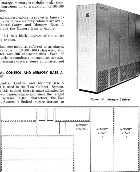
A typical memory cabinet is shown
i
n figure
I-I.
Two types of core memory cabinets are
avail-able: Central Control and Memory Base A
c
abinet and the Memory Base B cabinet
.
Figure 1-4 is a block diagram of the entire
memory system.
Individual core modules, referred to as stacks,
are available in 10,000 (10K) character, 20K
character, and 30K character sizes. Each of
these stacks is completely independent,
contain-ing all necessary drivers, sense amplifiers, and
core.
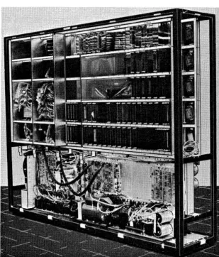
CENTRAL CONTROL AND MEMORY BASE A
CABINET
The Central Control and Memory Base A
cabinet is used in the Two Cabinet System.
Within this cabinet there is space allocated for
up to two memory stacks and since the largest
stack contains 30,000 characters, the Two
Cabinet System is limited in core storage to
SECTION
1
CORE MEMORY
60,000 characters. Figure 1-2 shows a layout
di-agram of the Central Control and Memory Base
A cabinet, and figure 1-3 shows the internal
hardware of the cabinet.
Figure 1 -1. Memory Cabinet
: - - - I
DO
r - - - -I -- - - , I r - - - -I ,- -r
1 :
I 1 I I I 1 I I
I 1 I
I I
I I
I I I I I
I I I
I :
t ___________________ I 1 1_ _ _ _ _ _ _ _ _ _ _ _ _ _ _ _ J I I
r - - - --,
l I D
I 1I
I I
I 1
L __________________ I~ _ _ _ _ _ _ _ _ _ -I
1- - -
-I
I I
----
----,
I
I
I I
L __________________________________ J
1--- --- - -- ---- --- ---..,
I I
I
I
I '- _ _ _ _ _ _ _ _ _ _ _ _ _ _ _ _ _ _ _ _ _ _ _ _ _ _ _ _ _ _ _ _ _ J I
1- - - ,
I 1
I 1
I I
I I
1 1
MEMORY
CONTROL MEMORY STACK
I
I I
I I
1
I
I
1 I II
II II
I II 1 I
I I I
MEMORY STACK
2
L _ _ _ _ _ _ _ _ _ _ _ _ _ _ _ _ _ _ _ _ _ _ _ _ _ _ _ _ _ - J L _____________ 1'- __ _
Figure 1-2. Central Control and Memory Base A Cabinet Layout
[image:9.824.125.720.222.952.2]Figure 1-3. Central Control and Memory Base A Cabinet
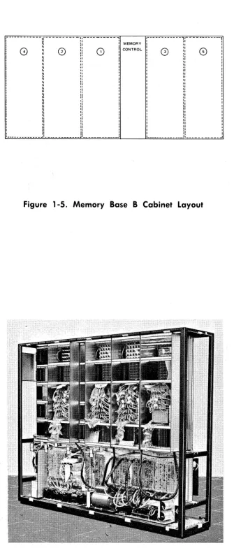
MEMORY BASE B CABINET
The Memory Base B cabinet houses up to five
memory stacks and provides these systems
with measurably more storage. Figure 1-5 is a
layout diagram of the Memory Base B cabinet
and figure 1-6 shows the internal hardware of
the cabinet.
Certain Models of the B 2500 and B 2700 are
configured into three cabinet systems (CPU
Peripheral Controls, and Memory Base).
Thes~
Systems operate with one Memory Base B
cabinet, with a maximum core storage of 120K
characters (four 30K stacks).
Additional models of the B 2700 and B 3500
Systems can each utilize up to four Memory
Base B cabinets. The first three cabinets, each
containing five 30K stacks, provide these
sys-tems with storage for up to 450K characters.
The fourth cabinet can house only up to 50K
characters, giving the system a total memory
storage capacity of 500K characters. The
memory stacks are placed in specific locations
within the cabinet as shown in the layout
diagram, figure 1-5. Each consecutive stack
area must contain a full 30K characters before
the next location can be utilized.
MEMORY STACKS
Figure 1-7 is a detailed block diagram of a core
memory stack with associated control circuits.
Each stack is self-sufficient in that it contains
all necessary timing circuits, drivers, and sense
amplifiers to be totally independent of all other
stacks. However, if the storage size of the core
memory is changed, the memory-size card,
lo-cated in the central processor, must be changed.
Stack Configuration
Each core stack is 17 planes deep (figure 1-8),
with each word containing one bit from each
plane. This results in a 16-bit (four digit) word
with one parity bit.
Each plane has its own sense and inhibits lines.
They share addressing lines for associated
loca-tions on the other planes.
Array positioning provides for coordinate
ad-dressing of the desired core position. Figure
1-9 is a block diagram showing the three types
of arrays: the 50 x 100 array for the 10,000
character stack, the 100 x 100 array for the
20,000 character stack, and the 100 x 150 array
for the 30,000 character stack.
For addressing purposes, each stack is divided
into 5,000 character sections referred to as
sextants. The 30,000 character stack (figure
1-9) contains six sextants, the 20,000 character
stack contains four sextants, and the 10,000
character stack contains two sextants
.
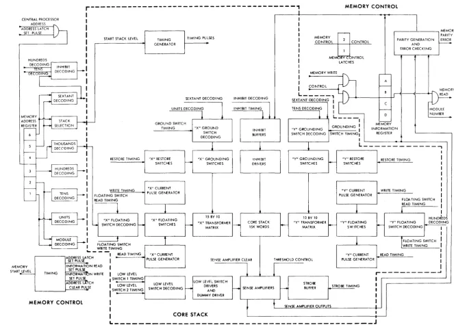
MEMORY CONTROL
The interface between memory control, central
processor and central control is shown in figure
1-10. Figure 1-11 is a detailed block diagram of
the memory control logic and the interfacing of
this logic to the memory stacks.
...
w
r---,
MEMORY CONTROLI CENTRAL PROCESSOR
ADDRESS
I
~
ADDRESS LATCH MEMOR
SET PULSE Y
START STACK LEVEL
HUNDREDS DECODING I
INHIBIT ItN) I G D E C O F DECODIN
~
SEmNTp-: DECODINGMEMORY
ADDRESS ~~ STACK REGISTER SELECTION
, - - - I
6 I
r--- I
5 tr-:HOUSANDS - DECODING
f-+
~; 4 RESTORE TIMING
'-~-H
HUNDREDS3 ~ 2 !---1 ~ ORY MEM STAR T~
DECODING
r--WRITE TIMING
~~~
FLOATING SWITCH DECODING READ TIMING-~-j
~:-
UNITS~ DECODING "X" FLOATING
c..., SWITCH DECODING
-~D~
---1DECODING FLOATING SWITCH --
...
_--
WRITE TIMINGI READ TIMING ADDRESS LATCH
.
SET PULSE I INFORMATION READ
I SET PULSE
TIMING INFORMATION WRITE I LOW LEVEL SET PULSE I SWITCH 1 TIMING ADDRESS LATCH
I LOW LEVEL CLEAR PULSE
I
SWITCH 2 TIMING
MEMORY CONTROL I
I
I
roo- PARITY
TIMING TIMING PULSES MEMORY 2 PARITY GENERATION ERROR
GENERATOR CONTROL CONTROL AND
-1 ERROR CHECKING
MEM~)NTROL
LATCHES
MEMORY WRITE r-~
A
CONTROL ~
(
B~
L _ _ _ _ _ ,
SEXTANT DECODING INHIBIT DECODING SEXTANT DECODING
I
I
INHIBIT TlMINGl
I
C
UNITS DECODING TENS DECODING I r--- MODULE
!
!
I L ____ D NUMBERt
I
MEMORY GROUND SWITCH
GROUNDING I TIMING "X" GROUND
INHIBIT "Y" GROUNDING I INFORMATION SWITCH BUFFERS SWITCH DECODING SWITCH TIMINGI REGISTER DECODING
I
L ____________ -,
"X" RESTORE "X" GROUNDING INHIBIT "Y" GROUNDING "Y" RESTORE RESTORE TIMING SWITCHES ~ SWITCHES
DRIVERS SWITCHES
-
SWITCHES"X" CURRENT
"Y" CURRENT WRITE TIMING PULSE GENERATOR
PULSE GENERATOR
FLat>. TING SWITCH
1
l
READ TIMING
!
15 BY 10 10 BY 10 HUNDREDS
"X" FLOATING
"X" TRANSFORMER CORE STACK "Y" TRANSFORMER "Y" FLOATING "Y" FLOATING DECODING SWITCHES f--
1-15K WORDS
r--
MATRIX f--- SWITCHES I-- SWITCH DECODINGMATRIX I
I
r
!
FLOATING SWITCH IWRITE TIMING I I "X" CURRENT "Y" CURRENT READ TIMING I PULSE GENERATOR SENSE AMPLIFIER CLEAR THRESHOLD CONTROL PULSE GENERATOR
I
1
r - - - ' II
LOW LEVEL SWITCH STROBE
LOW LEVEL DRIVERS STROBE TIMING I SWITCH DECODING f-- r-- SE NSE AMPLIFIERS
-
BUFFER IAND
DUMMY DRIVER I
f
I
SENSE AMPLIFIER OUTPUTS I
I
CORE STACK
.
L _ _ _ _ _ _ _ _ _ _ _ _ _ _ _ _ _ _ _ _ _ _ _ _ _ _ _ _ _ _ _ _ _ _ _ _ _ _ _ _ _ _ J
Figure 1-4. Memory Block Diagram
[image:11.794.60.723.59.533.2]--- -,i--- - - - )
I:
"
0) :: (2)
"
'I
"
"
"
""
"
"
"
"
"
"
" 'I
"
I, II II
"
II
"
"
"
,
:,
_____________ 1 ___________
11 ____ _--.
MEMORY CONTROL
:---1·
"
"
"
"
" " " ""
I 1:
1 ____________ J: ________ _
Figure 1-5. Memory Base B Cabinet Layout
Figure 1-6. Memory Base B Cabinet
-,
,,
I I I I
,
I I
gran ted, a series of address decoding
proce-dures are initiated. This addressing
ISper-formed in the following sequence:
a
.
Cabinet addressing.
b. Stack addressing.
c. Sextant addressing.
d. Location.
Figure 1-12 shows an exploded view of the
com-plete memory scheme. The first breakdown is
from the address in the address register (ADR),
located within the central processor, into
cabinet selection
.
Once the cabinet is located,
the stack within the cabinet is determined from
the address in the memory address register
(MAR). Next, the proper sextant is selected
and, with the last four digits in the MAR, two
transformers lines are selected: one "X" and one
"Y. "
Cabinet Addressing
Cabinet addressing is determined by the
decod-ing of the most significant digit (MSD) of the
address within the address register of the
proc-essor (ADR) when a memory access has been
granted. As the access is granted to either an
I/O channel or the central processor, a term
called memory start (MST) is gated with the
MSD in the ADR, which then sends the start
level to the proper cabinet.
Stack Addressing
Stack addressing is accomplished by gating
dig-its 5 and 6 of the memory address register with
the start stack timing level (SSTL). Since a stack
can contain up to 60,000 digits, stack number one
is selected when the MAR is from 000,000 up to
059,999; stack number two is selected when the
MAR is from 060,000 up to 119,999, etc. The
MAR values and address of stacks are as follows:
Value of MAR
000,000 - 059,999
060,000 - 119,999
120,000 - 179,999
180,000 - 239,999
240,000 - 299,999
Addressed Stack
1
2
[image:12.816.73.408.164.948.2] [image:12.816.79.398.596.950.2]ADDRESS & (SXn) DECODING
STACK START LEVEL
( S n S L) MEMORY TIMING
T R D A E
N
S C
ADDRESS ~ (SXh) 0
~~~-~~y~--~--~----
__
--~~ FDECODING 0 D
R'
MN
FRO M MEMORy
CONTROL
150
• 1/
E G
R
X ADDRESS
INHIBIT GATING
MIR GATING
MEMORY TIMING
SX1
C
SX2
S X 5
~y .,
_ 1 0 0 ADDRESS LIN E S
SX3
S
0
E A TOSX4 SENSE N M MIR
R
LINES(102)s
E S pE
S X 6
[image:13.613.52.566.86.539.2]4 - - - -68 INHIBIT LINES
Figure 1-7. Stack Block Diagram
Sextant Addressing
As previously mentioned, a sextant is a 5,000 character section of a stack with six sextants in a 30,000 character stack, four sextants in a 20,000 character stack, and two sextants in a 10,000 character stack. The sextants are desig-nated 1 through 6, depending on the stack size, as shown in figure 1-9. Since each of the five stacks have sextants 1 through 6, there are five groups of stack addresses which could select each sextant term. The proper sextant is deter-mined by digits 5 and 6 of the memory address register.
1-5
Sextan t one is selected by the term sextant 1 (SX1). This term is used to select the group of transformers that driv,es current through the selected sextant. Sextants 2 through 6 are selected in a similar manner by terms SX2 through SX6.
Location
As shown in figure 1-9, a full stack contains six sextants, with each sextant occupying a specific location within the stack. The stack is ad-dressed by 150 "X" address lines .and 100 "Y" address lines with each sextant having 50 intersecting "X" and "Y" lines.
Figure 1-8. Memory Planes
SX4 I
~/~-~ :
I
I I
I
I
!~
,1'
Each of these addressing lines is connected to the secondary of a transformer with a single transformer for each line. The selection of one "X" transformer and one "Y" transformer com-pletes the coordinate addressing of a specific lo-cation.
The selection of the proper transformer is ac-complished with the last four digits of the MAR and the sextant decoding described earlier. The sextant information divides the transformers into groups of 50. However, the "X" address line that intersects sextant 1 (SX1) also passes through SX3, as shown in figure 1-9. Similarly, the "X" address lines that intersect sextants 2 and 3 also pass through sextants 4 and 6, re-spectively. The "Y" address that intersects sextants 1 and 3 also passes through sextants 2 and 5, and 4 and 6, respectively.
Figure 1-13 shows that if the address in the MAR selects SX1, only the group of transfor-mers whose output lines pass through SX1 and SX3 for the "X" transformer matrix and
through SX1, SX2 and SX5 for the "Y" trans-former matrix are enabled. However, only SX1 experiences coordinate intersection, which means that only sextant 1 is provided with both "X" and "Y" half-current.
The summation of these two half-currents provides full current (2 times one-half), which is required to fully change the state of the core. The other sextants included with the transfor-mers that intersect SX1 only receive half of the required current, either from the "X" or "Y" transformer matrix.
The transformers are selected by the intersection of two address decoding lines. The "X" address lines are decoded from sextant MAR thousands and MAR units gating, where-as the "Y" address lines are decoded from the sextant, MAR hundreds, and MAR tens. Refer to figure 1-14. One group of address decoding lines is composed of the thousands position, dig-it 4 of MAR. Since digdig-it 4 can contain ten dif-ferent configurations (0 through 9), it is de-coded into ten different address decoding lines directly from the binary count in the MAR digit 4 position. These lines are designated KO, K1, K2 through K9.
The other group of 15 lines is composed of the unit sextant gating. The "X" transformers must address through different pairs of sextants. These five unit terms UO through U5, combined with the three sextant terms, gates the group of 15 lines to the transformer matrix. A com-plete block diagram of these lines and associ-ated gating is shown in figure 1-15. At the point of intersection of the decoding lines, a transfor-mer is selected. Only one horizontal line and one vertical line can be enabled during a memory access; therefore, only one transformer is enabled. This drives current through one "X" address line of the core stack.
"Y" TRANSFORMER
I
"Y" TRANSFORM ER "Y" TRANSFORMERMATRIX MATRIX MATRIX
"Y" "Y" "Y"
50
ADDRESS 50 50 50 50
LINES LINES ADDRESS ADDRESS
I--LlNES- r4'-LiNES-LINES LINES -LiNES-LINE S
r - - r
-"X" "X"
T T
R SEXTANT SEXTANT R SEXTANT SEXTANT "X" SEXTANT SEXTANT
A M I
I A 50 LINES I I I I
N A
S T 50 "X" I
I
N "X" I T T 50 "X" I TF R ADDRESS 1 2 S A 1 3 R ADDRESS 1 3
0 I LINES F D A LINES
R X D N
M 0 R
E R E S
R M S F
E S 0
R L R
I
M N
50 BY 100 ARRAY M E SEXTANT SEXTANT E SEXTANT SEXTANT
I
I
A S I I R
T 50 LINES
,
,
50 "x" Il
2 4 2
R M ADDRESS
I A LINES
X T
R
'
-I
100 BY 100 ARRAY X SEXTANT SEXTANT
I I
50 "X" I I
ADDRESS 5 6
LINES
I
I
'
-100 BY 150 ARRAY Figure 1-9. Address lines Through Sextants
The tens and units positions of MAR can de-scribe 100 different digit addresses. There are five word addresses in each 20 consecutive digit addresses starting with 000,000.
The first word of each 20 addresses contains an even digit (MAR tens equal to 0, 2, 4, 6 and 8). The odd MAR digits have a value of 0 through 3 for any digit address in the first word. The address of any digit in the first word is desig-nated by the term VO.
The second word of each 20 addresses contains an even (MAR 2, and MAR 1) digit value of 4 tbrough 7. The term for this decoding is V1.
The three remaining unit terms (2 through 5) are decoded in the same manner, generating the terms V2 through V 4.
1-7
The hundreds lines are decoded from the binary count in the hundreds position of the MAR. This count can be from 0 through 9, with each count being designated HO through H9. The output of the "Y" transformers passes through two groups of three sextants, as shown in figure 1-9. These groups form the terms SX1, SX2, or SX5 and SX3, SX4, or SX6, with each gate having five even tens terms to achieve the ten gating lines to the matrix. The even tens terms are decoded directly from the ten posi-tions of MAR minus the one bit used in the units gating. The terms TO, T2, T4, T6 and T8 are derived from this count. Refer to figure 1-9. Addressing is now complete. (The transfor-mers drive the address lines which select one specific location which contains one word or four digits, plus a parity bit. Examples of ad-dress breakdown are given in table 1-1.
[image:15.615.51.557.85.444.2]ADDRESS
I
I I I
I
I
I
I I I
I 1
1
I
I I I
I
I I
I I I
:
MEMORY
CONTROL
0
I
I
I I
I
I
IMEMORYJ
~--~I----~~~ADDRESS
lREGISTER
I
I
I I
I
~--_ _ ~II MEMORY ~~ __ ~
n
I N FORMATION~~-+l11 REGISTER
t--t-~U~OEN~~~~I
fl
LATCHES
A
MEMORY START
READ
I
I I
I
READ
WR I TE WRITE
CONTROL
J A
CONTROL
CONTROL
PERIPHERAL U NIT
•
,
I
MEMORYI
ADD R E S5
I
MEMORY
I
FLI P-FLOPCENTRAL
PROCESSOR
PRIORITY CONTROL
1/0
CONTROL
f
PR 10 R I TY I~___
----I~---~~I LOGIC
r
~---~CENTRAL
CONTROL
Figure 1-10. Memory Control Interface
Table 1-1. Examples of Address Breakdown
Address Cabinet Address Stack Sextant MAR MAR MAR Unit
in ADR Location in MAR Location Location Digit 4 Digit 3 Digit 2 Term
(Thousands (Hundreds (Tens
Term) Term) Terms)
183620 1 183620 4 1 K3 H6 T2 UO
382195 2 082195 2 3 K2 HI T8 U3
I
491835 2 191835 4 2 Kl H8 T2 U3
604171 3 004171 1 1 K4 HI T6 U2
895952 3 295952 5 6 K5 H9 T4 U3
[image:16.617.54.560.103.565.2];----CONTRO-L----l
I
S1:~SL
IISEXTANT NUMBER
S4 S L
STACK41
S 3 S L ,.--_ _ _ _ _ ... IL--_---'-'Ac:...;N'-='D'---'-'A=D=O.;..;R-=E....:::S'-'S'--~E _L_E.-C_T_I...;;O_N_~_ S X 1
S4 S L
~~I
SX3
SSSL
I
I ~ ~ ~ SX2 SX4 t---.
ISTACK
ISELECT
I
I
SEXTANT ~I
IADDRESS
I
DECODING LOGIC
.LEVELS _ __ r- _
~r--- \
I
STACK ~~DECOD ING 1_ ,
I
LOG I Cr
--,
i
START STAC K MEMORY ,...~...,...,...,I""""'-~..,
TIMING ADO RES 5
l
6 5 \4 3 2 \1 LEVEL REGISTERI
ADDRESS FROM PROCESSOR
MEMORY WRITE
BU~
CONTR~
"
,
... _M....;;C....:;(n....;.)....:B::...;U::...;S=---l¢
INHIBIT \ DECODING J
MEMORY READ BUS
MIU
A
~
B
... - - + i C
~
... - -... 0
I000o.-MEMORY
~
N:~~t.~~~I~N
CO NTROL /
SENSE AMPLIFIER NUMBER
CONTROL __
MEMORY
CONTROL DECODING
MEMORY ~---~ CONTROL
L
LATCHESI I I
I
'(MiRI
A,B,C,O) I BI SXS SX6
T
-S2SL
S T A C ,..K---.;;2~t--_ ...
~ ~--~I sx 1 SX3
I
~ ~ ~ S X2 S X4 I
-~~~~
4~
~
4~
4~
~ V ~
-f~
~
I SX5 SX6
T
-S 1 -S L
STACK 1
-
S X 1-
IN
~
H SX2 I
B I
T SXS
I000o.-S 3 S L STACK3'
5 X 1
,...
I
N
~
H S X 2 I
B
I
T SXS
I000o.-S 5 I000o.-S L
STACK 5
S X 1
r-r
N H---
SX2 I B IT SXS
I000o.-SX3 SX4 SX6 SX3 SX4 SX6
5 X 3
SX4
SX6
-Figure 1-11. Memory Control/Stack Interface
1-9
~~
7D-SENS E AM PL IFIER OUT PUTS
[image:17.613.49.568.77.614.2]MEMORY ONTROl
MEMORY CABINET
S X 1
S X3
SX2
SX4
S x S
SX6
'. x" LIN E
SEXTANT 3
lOCATION SX5 SX6
STACK 3
Figure 1-12. Addressing Sequence
5 X 1 5 X 3
SX2
SX5
y y
TRANSFORMERS TRANSF ORMERS
(50 liNES) (S 0 l i N E S)
\'x"
T
R
A N S SO
F SX1 SX3
0 I I N E 5 R
M E R 5
.
X "T
R A N 5 50
F SX2 5 X4
0 liNES R
M E R 5
-;;X-';-so S X S SX6 LIN E S
[image:18.613.66.521.100.242.2] [image:18.613.106.504.131.691.2]SEXTANT AND UNITS GATING (15 LINES)
5 5 5
LINES LINES LINES T
G H
A
0 SX1 SX2 SX5
T U
I S
N A
G N
D SX3 SX4 SX6
S
I
I
I
(10 LIN ES)
Figure 1-14. 15 x 10 "X" Transfer Array
PARITY
The memory system operates with odd parity. This stipulates that an odd number of bits is set for each word location. That is, if a word is placed in the memory information register (MIR), which contains an even number of bits set, the parity bit must also be set at the time
the word is written. If the word within the MIR
contains an odd number of bits, the parity bit need not be utilized.
MEMORY TIMING
The memory cycle is one microsecond in dura-tion. Logic generated within the central control, and which is then called to memory, synchro-nizes timing pulses between memory, the cen-tral control, and the cencen-tral processor. The time duration between clock pulses is 560 nanoseconds.
Memory timing is generated in both memory control and the stack. When a memory cycle is
required by the central processor or an 1/0
channel, the central processor triggers the tim-ing circuits located within memory control. The appropriate stack is selected by address decod-ing and its timdecod-ing circuits enabled by a Start
1-11
Stack Level (SnSL). This logic produces timing pulses required to control the stack function.
STACK TIMING
The timing generated by the stack timing logic is used to control the sequence of operations that causes read and write current to flow with-in the stack.
READ OPERATION
The address to be used during the read operation is received from the address register within the central processor and is stored in the memory address register (MAR). The MAR is decoded by the stack decoding logic and gated to produce one of five SnSL levels. This level, in turn, determines the stack to be used. The MAR is also utilized by the address and sextant decoding logic to determine the location within the stack that is to be utilized. This information is gated to all stacks within the memory cabinet, but it is usable only in the stack receiv-ing the SnSL level. After the stack is triggered by SnSL, the output from the sense amplifiers is sent to the memory iriformation register (MIR). The sense amplifier senses the status of the cores within the stack. The type of operation to be performed is stored in the
mem-)ry control latches (MeL), which is then de--.:oded and controls the input to the MIR. In the case of a read operation, the outputs from the sense amplifiers are gated to the MIR where they are then sent to the central control or cen-tral processor for usage.
WRITE OPERATION
For a write operation, the logic utilized for the read operation is valid, except that the MeL now contains codes for a write operation. The outputs of the sense amplifiers are inhibited and only the new information from the central control or central processor is latched in the MIR. The inhibit gating, in turn, controls the writing of the information within the MIR into a memory location addressed by the MAR.
[image:19.613.58.300.83.273.2]SX5 OR SX61\ u4
LJ
SX5 OR SX6f\
u3
LJ
SX5 OR SX6 [ \ u2
LJ
SX5 OR SX61 ,
u1
LJ
SX5 OR SX6 1 \ uO
I~
SX2 OR SX4
1'\
u4LJ
SX2 OR SX41\
u3
LJ
SX2 OR SX41\
u2
I~
SX2 OR SX4
1\
u1LJ
SX2 OR SX4!\
uO
LJ
SX1 OR SX3
f\
u4LJ
SX1 OR SX31 \ u3
LJ
SX1 OR SX3
1\
u2
LJ
SX1 OR SX3
1'\
u1
U
SX1 OR SX3
1\
uO
l )
KO K1 K2 K3 K4 K5 K6 K7 K8 Kg
-
--
--
-
-
-
-[image:20.617.52.558.102.716.2]
SX3, SX4, OR SX6 ... T8
l/
X4, OR SX6
D
T6 SX3, S
SX3, SX4, OR SX6 \ T4
J
SX3, S X4, OR SX6
"
T2
U
SX3, SX:~ OR SX6
D
X2, OR SX5
D
T8 SX1, S
SX1, SX2, OR SX5
\
T6
~
SX1, S X2, OR SX5D
T4
SX1, SX2, OR SX5
\
T2
J
X2, OR SX5
D
TO SX1, S
HO Hl H2 H3 H4 H5 H6 H7 H8 H9
-
-
-
--.- -
-
-
--
-Figure 1-16. "Y" Transformer Decoding Lines
[image:21.615.40.572.90.530.2]GENERAL
The Central Processors contain the circuitry and logic required to perform the instruction set utilized by their associated systems. These instruction sets are capable of performing oper-ations on digit-, byte-, or word-formatted data fields. The internal working code utilized by the central processors is 8-bit EBCDIC or 8-bit USASCII, both of which are programmatically selectable. Integrated into the. hardware is an automatic interrupt system capable of informing the processor of any condition experi-enced by any portion of the system.
The B 2500/B 3500 and the B 2700 Central Proc-essor speeds are as follows:
Model
B 2510/B 2520
B 2731
B 2501/B 2502/B 2741/B 27611
B 2540/B 2765
B 2751/B 2771/B 2772/B 35011
B 35061B 3508/B 3510/B 3514
PROCESSOR OPERATING MODES
Processor Speed 0.5 MHz 0.67 MHz
1.0 MHz
2.0 MHz
The Central Processors can operate in one of four modes: control state, zero base; control state, non-zero base; normal state, zero base; and normal state, non-zero base.
Control State, Zero Base
In this mode, the interrupt flip-flop can be set, but the interrupt branch is not executed until the return to normal state. Any privileged in-structions are allowed.
Control State, Non-Zero Base
In this mode, the interrupt flip-flop can be set, but the interrupt branch is not executed until the return to normal state. Any privileged in-structions are disallowed.
2-1
SECTION
2
CENTRAL PROCESSOR
Normal State, Zero Base
In this mode, the interrupt branch is allowed to be executed and privileged instructions are allowed.
Normal State, Non-Zero Base
In this mode, the interrupt branch is allowed to be executed and privileged instructions are disallowed.
Object program, assemblers, compilers, and generators are executed in the normal state, non-zero base, whereas the greater majority of the Master Control Program (MCP) is executed in the control state, zero base. A small number of privileged instructions, used exclusively by the MCP, can be executed only in zero base. These priviledged instructions include opera-tions such as initiate output and read timer.
LOGICAL UNITS
There are several logical units contained within the central processor that directly or indirectly affect its operation. These logical units control the execution of specific instructions and are, themselves, set or changed by other instruc-tions.
OVERFLOW Flip-Flop
The OVERFLOW flip-flop is a hardware logical unit that indicates the data field of a move or arithmetic instruction is exceeded. If an over-flow condition is detected, the command is executed but the data is not affected. The OVERFLOW flip-flop is not cleared at the be-ginning of an arithmetic operation but is pre-served; therefore, it indicates overflow that has occurred any time before or during a series of arithmetic operations or other interjected non-arithmetic operations. Instructions that can create an overflow condition are:
a. Arithmetic instructions except multiply. b. Floating point arithmetic instructions. c. Move Numeric.
d. Move Alphanumeric.
Overflow cannot occur during a multiply in-struction, since the receiving field is always large enough to contain the product. In all cases except the floating point instructions, overflow results when the receiving field cannot contain the sending field. With floating point instruc-tions, the overflow can also be caused by an out-of-range exponent. The OVERFLOW flip-flop is reset by the Branch-On-Overflow in-struction. Once cleared, it can be set if the con-ditions arise while executing those instructions that may cause it to be set. There are two ways in which the present setting of the OVERFLOW flip-flop may be stored in the four-bits of re-served address memory and then cleared, as shown below.
a. Branch Communicate.
b. Automatic interrupt feature.
The OVERFLOW flip-flop is restored from the reserved memory location by the Branch Reinstate instruction. In addition, the object program may branch to some subroutine and the OVERFLOW flip-flop setting must be re-tained and restored at the conclusion of the sub-routine execution, prior to continuing in the ob-ject program. The Enter instruction stores the flip-flop setting into the four bits of the re-served character location in the memory stack, and then clears the OVERFLOW flip-flop. The Exit instruction restores the OVERFLOW flip-flop setting from this reserved location.
COMPARISON Flip-Flops
Two hardware flip-flops make up the comparison logical unit. These two flip-flops have the following four combinations (0 = reset, 1 = set):
a. 00 - cleared.
b. 01 - greater or high comparison result. c. 10 - less or low comparison result. d. 11 - zero or equal comparison result. These four states represent the result of execu-ting an instruction that affects these logical units. The cleared state actually indicates that there is no comparison result existing. The in-structions that set a result into the
COMPARISON flip-flops and are reflected on the appropriate console indicators are as fol-lows:
a. All arithmetic instructions. b. All floating point instructions. c. Compare instructions.
d. Move Numeric instruction. e. Move Alphanumeric instruction. f. The bit test instruction.
g. The logical instructions. h. The scan instructions.
1. The Edit instruction.
J. The Scan Result Descriptor instruction. k. Search instruction.
Any branching that is done on the basis of the comparison will not change the status of the flip-flops. Only another instruction that affects them can change their status. When entering control state by means of the Branch Communi-cate instruction or the automatic interrupt sys-tem, the status of the comparison flip-flops is stored. The 2-bit and I-bit of the same charac-ter that stores the OVERFLOW flip-flop status will contain the status of the COMP ARISON flip-flops. The flip-flops are then cleared before branching to control state. When return is made to the normal state, the Branch Reinstate instruction will restore the comparison flip-flops from the character in reserved address memory. Similarly, when entering a subrou-tine, the Enter instruction stores the COMP AR-ISON flip-flops in the 2-bit and I-bit of the specified character in the memory stack. This same character contains the OVERFLOW flip-flops status. When leaving the subroutine with the Exit instruction, the COMPARISON flip-flops are restored from this character in the stack.
EBCDIC/USASCII Mode Flip-Flop
indi-cates that the processor is using the EBCDIC code. The flip-flop can be programmatically set to indicate that the processor is to use USASCII code. The Set Mode instruction sets or resets this flip-flop, as desired by the programmer. The following instructions are sensitive to the setting of the EBCDIC/USASCII mode flip-flop:
a. All Arithmetic instructions.
b. All Floating Point instructions.
c. Move Numeric instruction.
d. Move Alphanumeric instruction.
e. Move Repeat instruction.
f. Translate instruction.
g. Scan Delimiter Equal instruction.
h. Scan Deliml\ter Unequal instruction.
i. Edit instruction.
When branching to the control state, the setting of the EBCDIC/USASCII MODE flip-flop is al-so stored in the 8-bit of the same character con-taining the settings of the OVERFLOW and
COMP ARISON flip-flops. It is then cleared
pri-or to entering the control state. This is done by either of the following instructions:
a. Branch Communicate.
b. Automatic interrupt branch.
When returning to normal state, the Branch Reinstate instruction will restore the EBCDIC/ USASCII mode flip-flop from the character in reserved address memory. When entering a subroutine, the Enter instruction will store the status of the MODE flip-flop in the 8-bit of the specific character in the stack which also con-tains the OVERFLOW and COMPARISON flip-flop settings. The Exit instruction will restore the EBCDIC/USASCII MODE flip-flop from the character in the stack when leaving the sub-routine. This is necessary in the event that the flip-flop is changed by the subroutine. The spe-cial character in reserved memory or the stack contains the setting of the EBCDIC/USASCII mode flip-flop in the 8-bit, the setting of the
2-3
OVERFLOW flip-flop in the 4-bit, and the set-tings of the COMPARISON flip-flops in the 2-bit and l-2-bit.
INTERRUPT Flip-Flop
The INTERRUPT flip-flop is a hardware logical unit that indicates the presence of an interrupt. This flip-flop controls the automatic interrupt circuitry when the processor is operating in
normal state. If the flip-flop is reset (no
inter-rupt condition), execution continues in sequence
from instruction to instruction. If an interrupt
occurs, the flip-flop is set. If the flip-flop is set
at the completion of an instruction execution cycle, the automatic interrupt branch to control state, base zero occurs. The flip-flop is set by the detection of any I/O complete interrupt. The Scan Result Descriptor instruction will re-set the INTERRUPT flip-flop while executing the interrupt handling routine.
Normal/Control State Flip-Flop
This flip-flop can be set only by the Branch Reinstate instruction which is executed by the
Operating System. It is reset by either the
Branch Communicate instruction or the auto-matic interrupt branch. When the flip-flop is set, the processor is operating in the control state which inhibits the automatic interrupt cir-cuitry.
The setting of this flip-flop dictates the state of operation of the processor. When it is set, the processor is operating in normal state and al-lows the execution of the automatic interrupt branching.
Timer
The timer consists of two words in address memory. The first timer word is counted at a one KiloHertz rate. This word is compared with the value of the second word which is placed there by the Operating System. When the first word is equal to or greater than the second word, a clock interrupt occurs. The timer will continue to count after the interrupt and re-quires the Operating System to read and clear the first word of the timer. The value read from the timer word is used by the Operating System for logging functions and updating the real-time clock.
Base Register
The base register in the processor is a three-dig-it register. These three digthree-dig-its are always added to the two high-order digits of the five-digit program and instruction address to form a six-digit absolute address. This makes the base reg-ister modulo 1000, that is, a base regreg-ister value of 137 is actually 137,000. This base register val-ue is always added to the ba'se relative address contained in the instructions. This computation takes place during the fetch cycle, prior to stor-ing the absolute address generated into address memory. For any program, the base register value is created by the Operating System and stored in reserved memory location 000070 (ta-ble 2-1) prior to initiating the program. When the Branch Reinstate instruction is executed, the base register is set to the value contained in reserved memory, establishing the base reg-ister of the normal state program. If a Branch Communicate instruction or an automatic inter-rupt branch is executed, the base register value is stored in the reserved address memory loca-tion prior to entering control state and the base register is also cleared to zero.
Limit Register
The limit register within the proceSS0r is a three-digit register. The purpose of the limit register is to provide memory protection. Mem-ory protection is accomplished by comparing the high-order three digits of the absolute ad-dress generated for instructions with the base and limit registers. The base register provides the lower limit and the limit register provides the upper limit. The value of the limit register is provided by the Operating System and stored in reserved memory location 000073. The Branch Reinstate instruction sets the limit reg-ister to the value contained in reserved memory. When the Branch Communicate in-struction or automatic interrupt branch is executed, the limit register value is stored in re-served memory prior to pntering control state and the limit register is set to the system mem-ory size. This allows the Operating System to access all memory.
Index Registers
The index registers used in the processors are not hardware registers as are the base and limit registers. Three index registers are contained in
reserved locations of an object program and are always assigned the same base relative address. The format of the index register is shown in fig-ure 2-1.
~I
011
02I
03I
041
05I
06I
07I
08I~
~~~---~---
I ' -0 '-- INDEX VALUE SIGNFigure 2-1. Index Register Format
Each index register consists of eight digit posi-tions. The most significant digit (D1) is the sign of the index value. The second digit position is not used when indexing. The value of the index is the decimal value contained in the remaining six digit positions (D3 through D8). If an in-struction address specifies indexing, the value of the specified index register is added algebraically to the base register, plus the base relative address prior to storing the generated address in address memory. The index register value can be changed by any instruction that addresses memory. In addition, the Enter and Exit instructions use and alter the setting of In-dex Register 3 (IX3); h9wever, the settings are saved and restored. In the zero-base state, the Scan Result Descriptor instruction and the Search instruction use IX1 in their execution.
DATA MODES
Two data modes are utilized in the Processors to represent internal data: the 4-bit mode and the 8-bit mode.
Four-Bit Mode
[image:26.612.326.532.184.246.2]Binary
Code Sign Code
Decimal Equivalent 0000
0001 0010 0011 0100 0101 0110 0111 1000 1001 1010 1011 1100 1101 1110 1111
+
+
+
+
+
+
+
+
+
+
+
+
+
+
+
o
1
2
3
4
5 6
7
8 9
.-ff (undigit 0)
*
..l' (undigit 1)*
Z (undigit 2)
*
% (undigit 3)
*
k (undigit 4)
*
.k (undigit 5)
*
*
These units are accepted by the arithmetic unit but they will result in unspecified results.When a signal 4-bit format is specified in the receiving field for any operation, a plus sign compares higher than a minus sign in the sys-tem's collating sequence, as shown below:
USASCII Code EBCDIC Code
+
1011+
= 1100- = 1101 - = 1101
Eight-Bit Mode
In an 8-bit mode, data is interpreted in units of 8-bits (one byte). Any required conversion be-tween 4-bit and 8-bit mode is accomplished au-tomatically during the execution of instructions with no timing costs absorbed by the program being operated.
2-5
For code sensitive instructions including the manipulation of 4-bit numeric data, the most significant fours bits of a 2-byte receiving field are automatically set to the code indicating the numeric subset of the selected 8-bit code. The four bits are 1111 (un digit 5) in EBCDIC code and 0101 (binary 5) is USASCII code.
Except in the move alphanumeric, move numer-ic and edit instructions, 8-bit data is considered unsigned.
Alphanumeric comparisons are performed in bi-nary code. The collating sequence for EBCDIC code is special characters, alphabetical charac-ters, and then digits. The collating sequence for USASCII is special characters, digits, and then alphabetical characters.
INSTRUCTION FORMAT
The two instruction formats used by the proces-sors are format A, which is variable in length from one to four syllables, or format B, which is a fixed length of eight digits. Most instruc-tions consist of from one to four syllables, de-pending on the particular instruction. An in-struction syllable consists of six digits as shown in figure 2-2.
The first syllable of every instruction contains the operation code in digits D1 and D2. Digit positions D3 through D6 have various functions as specified by each instruction. Generally, D3 and D4 specify the length of the A field, where-as D5 and D6 specify the length of the B field. Several instructions consist of a single syllable. In multiple syllable instructions, the second, third, and fourth syllables are the A field, B field, and C field addresses, respectively. The addresses always address the most significant digit of the field. Digits D7, D13, and D19 specify various control functions with respect to the A, B, and C field addresses, respectively. The two address-index bits determine which in-dex register, if specified, to use in generating the absolute address. The two address-control-ler bits specify whether signed or unsigned 4-bit or 8-4-bit formatted information is in the data field. The address controller bits may also spec-ify indirect addressing. Digits D3 and D4 of the first syllable can specify that the second sylla-ble (D7 through D12) is a literal value and not an address. The format of the literal is given in digits D3 and D4.
SYLLABLE 1
---~---/
D1 D2 D3 D4 D5 D6
T
AS SPECIFIED BY INSTRUCTION
SYLLABLE 3
D14 D15 D16 D17
SYLLABLE 2
D8 D9
842184218421842184218421
L
'A ADDRESS
L
A ADDRE:S
CONTROLLER
A ADDRESS
INDEX SYLLABLE 4
D20 D21 D22 D23
BINARY VALUES
BINARY
VALUES 842184218421842184218421842184218421842184218421
I
L
~
ADDRESS
I
B ADDRESS '
It:.
~
ADDRESS
'Ie
ADDRESS '
CONTROLLER CONTROLLER
B ADDRESS C ADDRESS
INDEX INDEX
Figure 2-2. Six-Digit Instruction Format
The 8-digit format is used only when an operation code and address are necessary, such as in a Branch instruction. The 8-digit instruc-tion format is shown in figure 2-3.
Address Index
The two most significant bits (8 and 4) of the first digit in the address field is the address in-dex control. The bit configuration of the address
index signifies which of three index registers is to be used while generating an absolute address. The eight-bit and four-bit configuration is as follows:
a. 00 - no indexing.
b. 01 - index register 1 (IXl).
c. 10 - index register 2 (IX2).
d. 11 - index register 3 (IX3).
l,l,I,T,I,Y,I,Y,I,D
r
,I,Y,I'T,I,D/8,1
'8 42 1 8 42 1 8 42 1 8 4 2 1 8 42 1 8 42 1 8 42 1 8 42 1 BIN A RY VA LU E S
~
II
~DDRESS
OR~
ADDRESS 'OPERATION CONTROLLER
CODE ADDRESS
INDEX
[image:28.618.58.553.76.407.2] [image:28.618.109.498.573.711.2]There is an address index controller for the A, B, and C address fields, and also for the address field of the eight-digit instruction. If indexing is specified, the designated index register value contained in reserved locations within an object program is added algebraically to the address field and base register during the fetch cycle, prior to storage in its reserved address memory location.
Address Controller
The two low-order bits (2 and 1) of the first dig-it in the address field specify the data field for-mat. The address controller bits and address in-dex bits comprise the entire first-digit position of the address field. Four different two-bit and one-bit combinations can be specified by the two address controller bits as follows:
a. 00 - unsigned four-bit format.
b. 01 - signed four-bit format.
c. 10 unsigned eight-bit format.
d. 11 - indirect address.
Most signifi-can t address digi t for the branch in-structions
Any combination may be used except where prohibited by a specific instruction. The unsigned 4-bit format means that the data field consists of digits of information without a sign digit. The signed four-bit format specifies a dig-it data field wdig-ith a sign digdig-it preceding the most significant digit of the field. The field length does not include the sign digit position when a signed data field is specified. A bit con-figuration of 1101 is always treated as a minus sign (-), whereas any other bit configuration is considered as a plus sign (+). The unsigned eight-bit (character/byte) format specifies that the data field is in an internal eight-bit alpha-numeric code. The indirect address bit configuration specifies that the data field ad-dress is located at the specified base relative lo-cation. During the fetch cycle, another access must be made to obtain the specified field ad-dress.
An indirect address must be even and is checked after indexing, if any. An odd indirect
2-7
address is considered to be a non-synchronized address contained in an instruction and causes a processor in terru pt.
Address Digits
Since the first digit of the address field com-prises the address index and controller bits, five digits remain for use as the data field address; however, addresses may generate beyond this seemingly maximum address of 099,999 by
utiliz-ing the address controller bits at binary values up to a 2, thus creating an actual maximum ad-dress range per program of 000000 to 299,999. Programs exceeding the address of 099,999 can-not contain referenced data areas in excess of the 099,999 address. This address is always base relative and is added to the base register value during the fetch cycle. The absolute address stored in address memory is comprised of the value in the address field added to the base reg-ister. It can also be indexed by an index register when specified. The address digits are limited to the decimal digits zero through nine, thus creating a completely decimal addressing scheme for a beneficial system/programmer/ operator interface.
Operator Code
The first two digits of the first syllable repre-sent the operator code. This operator code is a decimal value ranging from 00 through 99, but all values are not used. All unassigned codes are reserved for expansion. If the processor receives any operator code that has not been assigned, an invalid instruction interrupt is generated. The operator code itself determines the number of syllables that must be fetched.
Field Length
For a majority of the instructions, the third, fourth, fifth, and sixth digits (D3 through D6) of the first syllable control the field lengths of the data fields (see figure 2-4). Digits D3 and D4 determine the A field length (AF), whereas digits D5 and D6 determine the B field length
(BF).
The field length values can range between 00 and 99, inclusively. If a field length of 00 is specified, the field length is 100. The digits D3 and D5 may also specify an indirect field
length. This is accomplished by making the D3/ D5 8-bit and 4-bit both equal to a 1. The base relative indirect address of the field length is obtained from the two low-order bits of D3/D5 and the even values of the D4/D6 digit. Thus, the indirect field-length base relative address can be any even value from 00 through 38 for a total of 20 base relative addresses.
03 04 05 06
8 BIT 4 BIT 2 BIT
1 BIT
[image:30.617.94.251.216.328.2]AF BF
Figure 2-4. Field Length Digits
Literal Specifications
Some of the instructions allow the A field length digits to specify that the A address syllble contains a literal value and not the ad-dress of a data field. Figure 2-5 shows the bit configuration for the various literals that the A address syllable can contain.
When D3 has the 8-bit and 2-bit ON with the 4-bit OFF, the A address is a literal. The D3 1-bit and D4 8-bit specify the format of the lit-eral. When the literal specification is an unsigned four-bit format, the literal length can
D3 04 03
8 BIT X x
4 BIT
2 BIT X LITERAL
LENGTH x
1 BIT
be one through six - the total number of digits in the address field. When the signed four-bit format is specified, the literal length can be one through five since the most significant digit is the sign digit:
When the eight-bit format is specified, the lit-eral length can have a value of one through three. If the literal length is less than the maximum length for the specified format, the literal is always assumed to be left-justified.
Read-Only Memory
The read-only memory (ROM) within the proc-essor is a resistive-type of storage. It contains a set of microprograms that controls most of the actions taken by the processor. The micro-programs are initiated by the operation codes of program instructions after they are fetched from memo"ry. The microprograms utilize the addresses stored in address memory during the execution of the instruction.
HARDWARE INSTRUCTIONS
The following list is a composite of all mnemon-ic operation codes used by the systems proces-sor. Assemblage of this list is only by general classification of the individual codes.
Each operation code will be broken down into its associated descriptor.
Data Movement 0 peration Codes
The following operator codes are utilized to ma-nipulate data to and from different areas with-in the system.
D4
x
~
LITERAL LENGTH03
x
x
x
04
~
LITERAL LENGTHUNSIGNED SIGNED UNSIGNED
4-BIT 4-BIT 8-BIT
FORMAT FORMAT FORMAT