Design of IIR Systolic Array Architecture by using Linear
Mapping Technique
Manoj Kumar
Department of ECE, NIT Manipur, Imphal, India
ABSTRACT
Design of IIR (infinite impulse response) systolic array architecture by using linear mapping technique is proposed in this paper. Systolic array architecture maps high level computations into hardware structures. In a systolic array, all the processing elements (PEs) are uniform and fully pipelined. On regular dependence graph, systolic architectures are designed by using linear mapping techniques. IIR filters are used in digital signal and image processing applications. IIR filters are recursive filters. IIR filters have high selectivity and less number of coefficients than the FIR (finite impulse response) filters. Various IIR systolic arrays architectures such as design B1, design B2, and design F is proposed in this paper. By selecting the projection vector, processor vector and scheduling vector these designs are derived.
General Terms
Linear mapping technique, Hardware utilization efficiency (HUE)
Keywords
Systolic array, DG, PEs, FIR, IIR, DSP
1.
INTRODUCTION
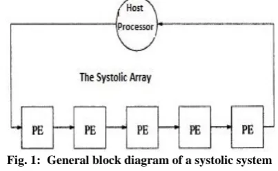
Dependence of the computations in an algorithm (program) is represented by the dependence graph. It is a directed graph. Computations in an algorithm are represented by nodes in the dependence graph (DG). And precedence constraints among nodes are represented by edges in a dependence graph. For a given algorithm a new node is created whenever new computation is called in a dependence graph. In a DG, no node is ever reused on a single computation basis. DG does not contain any delay elements for storing and passing data from the current iteration tosubsequent iteration. We can use the dependence graph for designing a systolicarray. Systolic arrays consist set of processing elements (PEs) to represent a network. In such system data move between processing elements in a rhythmic fashion [1, 2].Each processor are independent for storing and computing data. To maintain a regular flow in a systolic array, processing elements regularly pump data into and outside of the systolic system. The coprocessor can be used as a systolic array. The coprocessor can be combined with a host computer for passing data through processing elements. And the final result is returned to the host computer for maintaining the regular flow of data in the systolic array. A general block diagram of systolic array is shown in the Fig. 1. Important properties of systolic arrays are modularity and regularity. IIR filters are recursive filter with fewer design parameters, less memory requirements and lower computations complexity than FIR (Finite impulse response) filters. IIR filters are more attractive for designing filters where there is no requirement for a linear –phase characteristics within the pass-band of a digital filter [3]. General IIR filter equation is given below [4].
y(n)= + (1.1)
[image:1.595.327.529.370.494.2]
In Eq.(1.1) , N represents order of the filter. Many researchers have used IIR filters to implement image processing and digital processing systems. FPGA implementation of 1st-order 4D IIR frequency-hyperplane digital filters was proposed in 2011[8]. D.Dansereau and L.Bruton proposed a 4D frequency-planar IIR filter for light filed processing application [9]. Siji P.V and Manju Manuel used 2D IIR filters for directional filtering of temporally broadband bandpass space time plane waves [10]. An IIR filter design using CSA (Carry save adder) for DSP (Digital signal processing) applications was proposed in 2015[11]. In this design, high speed 2nd order infinite impulse response (IIR) filter was used to remove noise in signals. This paper is organized as follows. Section II discusses linear mapping technique. Section III presents the proposed different types of 1st order 1D IIR systolic arrays architectures. Section IV presents the proposed 2nd order 1D IIR systolic arrays architectures. In section V, the conclusion is presented.
Fig. 1: General block diagram of a systolic system
2.
IIR SYSTOLIC ARRAY DESIGN
METHODOLOGY
Linear mapping technique is used to design systolic array architecture [5, 6]. Linear mapping technique maps an N-dimensional dependence graph to a lower N-dimensional systolic architecture. If the presence of an edge in a certain direction at any node in the dependence graph represents the presence of an edge in the same direction at all nodes in the DG, then dependence graph is said to be regular. In a DG, at t=0, plane corresponds to a space representation where no time instance is assigned to any computation. Space representation is transformed to a space-time representation by using linear mapping technique. In space-time representation, each node is mapped to a certain processing element, and each node is executed at a certain time instance. Projection, processor space, and scheduling vectors are used to design systolic array and they are defined below [7]. Projection vector (d) is represented by the below matrix d =
The same processor is used to execute two nodes, which are displaced by d or multiples of d.
Processor space vector (PT) is defined below PT = [P1, P2]
PTI = [P1 P2]
Scheduling vector (ST) is represented by ST = (S1 S2). A node IT = (i,j) will be executed at time STI.
Hardware utilization efficiency (HUE) is defined as HUE =
Two tasks executed by the same processor are spaced |ST d| time units.
By selecting different projection, processor space, and scheduling vectors many systolic architectures can be designed. Following constraints must be satisfied by these vectors.
PTd = 0, i.e. two nodes are executed by the same processor if they are differ by projection vector d. STd ≠ 0, i.e. two nodes cannot be executed at the same time if they mapped to the same processor.
3.
1
StORDER IIR SYSTOLIC ARRAYS
Different design based on linear mapping technique for 1st order IIR filter is discussed in this section.
3.1
Design B
1Following values for projection vector, processor space and scheduling vector are taken for deriving the systolic design B1.
d = , PT = (0 1) , ST = (1 0) So, for any given node IT = (i,j) PTI = (0 1) = j
STI = (1 0) = i and STd = (1 0) = 1 So, HUE = = 1
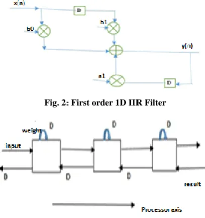
1st order 1D IIR filter is defined as Y(n) = a1 y(n-1)+ b0 x(n)+b1 x(n-1)
Block diagram for this filter is shown in Figure 2. Table 1 represents edge mapping for the design B1. For 1st order IIR filter, the block diagram for B1 systolic array design is shown in Figure 3 .Systolic array architecture for the design B1 is shown in Figure 4. And Figure 5, shows space-time representations diagram for the designing B1.From this figure, it is clear that input data is broadcast to the processors, weight values stay and output is appearing at the processors at different space and time.
Fig. 2: First order 1D IIR Filter
[image:2.595.343.519.78.171.2]Fig. 3: Block diagram of the B1 design
Fig. 4: Systolic array architecture of the design B1
Table 1. Edge Mapping Table for Design B1
e PT e STe
wt(1, 0) 0 1
i/p (0, 1) 1 0
result (1 , -1) -1 1
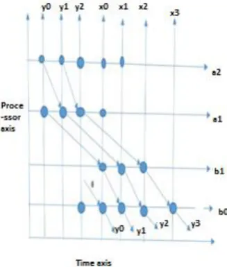
Fig. 5: space-time representation of the B1 design
3.2
Design B
2Following values for projection vector, processor space and scheduling vector are taken for deriving the systolic design B2.
d = , PT = (1 1), ST = (1 0) So, for any given node IT = (i,j) PTI = (1 1) = i+j
STI = (1 0) = i and STd = (1 0) = 1 So, HUE = 1
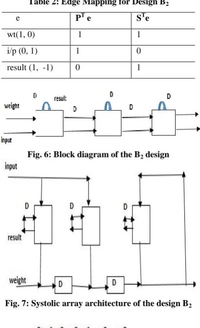
Table 2 represents edge mapping for the design B2. For 1st
order IIR filter, the block diagram for B2 design is shown in
Figure 6. Systolic array architecture for the design B2 is
[image:2.595.326.526.178.456.2] [image:2.595.62.266.534.751.2]Table 2: Edge Mapping for Design B2
e PT e STe
wt(1, 0) 1 1
i/p (0, 1) 1 0
result (1, -1) 0 1
[image:3.595.66.271.76.411.2]Fig. 6: Block diagram of the B2 design
Fig. 7: Systolic array architecture of the design B2
Fig. 8: Space-time representation of the B2 design
3.3
Design F
Following values for projection vector, processor space and scheduling vector are taken for deriving the systolic design F. d = , PT = (0 1) , ST = ( 1 1)
So, for any given node IT = (i, j) PTI = (0 1) = j
STI=(11) =i+j and STd = (1 1) = 1 So, HUE = 1
For the given 1st order 1D IIR filter Y(n) = a1 y(n-1)+ b0 x(n)+b1 x(n-1)
Table 3 represents edge mapping for the design F. For 1st order IIR filter, the block diagram for systolic array design F is shown in the Figure 9. Systolic array architecture for the design F is shown in Figure 10. And Figure 11, shows
[image:3.595.322.529.114.435.2]space-time representations diagram for the designing F. From Table 3, it is clear that weight value stays, input vector moves from left to right with 1 delay element and output moves from right to left with no delay elements.
Table 3: Edge Mapping for Design F
e PT e STe
wt(1, 0) 0 1
i/p (0, 1) 1 1
result (1, -1) -1 0
[image:3.595.65.271.412.565.2]Fig.9: Block diagram of the F design
Fig. 10: Systolic array architecture of the designF
Fig. 11: Space-time representation of the F design
4.
2
ndORDER 1D IIR SYSTOLIC
ARRAYS
Different design based on linear mapping technique for 2nd order IIR filter is discussed in this section.
4.1
Design B1Following values for projection vector, processor space and scheduling vector are taken for deriving the systolic design B1.
STI=(10) =i
and STd = (1 0) = 1 So, HUE = = 1
2nd order 1D IIR filter is defined as
Y(n) = a1y(n-1)+a2 y(n-2)+b0 x(n)+ b1x(n-1)
[image:4.595.345.509.80.273.2]Block diagram for this filter is shown in Figure 12. Table 4 represents edge mapping for the design B1. For 2nd order IIR filter, the block diagram for B1 design is shown in Figure 13. Systolic array architecture for the design B1 is shown in Figure 14. And Figure 15, shows space-time representations diagram for the designing B1.From this figure, it is clear that input data is broadcast to the processors, weight values stay and output is appearing at the processors at different space and time.
[image:4.595.60.273.240.416.2]Fig.12: Second order 1D IIR Filter
Table 4: Edge Mapping Table for Design B1 (2nd order)
e PT e STe
wt(1, 0) 0 1
i/p (0, 1) 1 0
result (1 , -1) -1 1
Fig.13: Block diagram of the B1 design (2 nd
order)
Fig. 14: Systolic array architecture of the design B1(2nd
order)
Fig. 15: Space-time representation of the B1 (2 nd
order) design
4.2
Design B
2Following values for projection vector, processor space and scheduling vector are taken for deriving the systolic design B2.
d = , PT = (1 1) , ST = (1 0) So , for any given node IT = (i,j) PTI = (1 1) = i+j
STI=(10) =i
and STd = (1 0) = 1 So, HUE = 1
For the given 2nd order 1D IIR filter Y(n) = a1y(n-1)+a2 y(n-2)+b0 x(n)+ b1x(n-1)
[image:4.595.64.271.432.580.2]Table 5 represents edge mapping for the design B2. For 2nd order IIR filter, the block diagram for B2 design is shown in Figure 16. Systolic array architecture for the design B2 is shown in Figure 17. And Figure 18, shows space-time representations diagram for the designing B2. From this figure, it is clear that input data is broadcast to the processors, output stay and weight value appear to the processors at different space and time.
Table 5: Edge Mapping Table for Design B2 (2nd order)
e PT e STe
wt(1, 0) 1 1
i/p (0, 1) 1 0
result (1, -1) 0 1
[image:4.595.323.531.563.689.2]Fig. 17: Systolic array architecture of the design B2 (2nd
order)
Fig. 18: Space-time representation of the B2 (2nd order)
design
4.3
Design F
Following values for projection vector, processor space and scheduling vector are taken for deriving the systolic design F. d = , PT = (0 1) , ST = ( 1 1)
So, for any given node IT = (i,j) PTI = (0 1) = j
STI=(11) =i+j and STd = (1 1) = 1 So, HUE = 1
For the given 2nd order 1D IIR filter Y(n) = a1y(n-1)+a2 y(n-2)+b0 x(n)+ b1x(n-1)
Table 6 represents edge mapping for the design F. For 2nd order IIR filter, the block diagram for design F is shown in Figure 19.Systolic array architecture for the design F is shown in Figure 20. And Figure 21, shows space-time representations diagram for the designing F. From Table 6, it is clear that weight value stays, input vector moves from left to right with 1 delay element and output moves from right to left with no delay elements.
Table 6: Edge Mapping Table for Design F (2nd order)
e PT e STe
wt(1, 0) 0 1
i/p (0, 1) 1 1
result (1, -1) -1 0
Fig. 19: Block diagram of the F design (2nd order)
Fig. 20: Systolic array architecture of the design F(2nd order)
Fig. 21: Space-time representation of the F(2nd order) design
5.
CONCLUSION
In this paper, different IIR systolic arrays are proposed.1st
order and 2nd order IIR filter examples are taken for designing the systolic arrays. Systolic array architectures for the different design are shown in the figures. For the proposed designs, space -time representation figures are presented. Also, edge mapping tables for IIR systolic array design are presented. Hardware Utilization Efficiency of the proposed IIR systolic array was one.
6.
REFERENCES
[1] H.T.Kung and C.E.Leiserson, “Systolic arrays (for VLSI),” in Sparse Matrix Symposium, SIAM, pp.256-282, 1978.
[2] H.T.Kung,” Why systolic architectures? IEEE Commuters Magazine, vol.15, pp.37-45, Jan. 1982. [3] Dimitris G. Manolakis,John G. Proakis,:Digital Signal
Processing: Principles, Algorithm, and Applications”, Macmillan Publishing Company, 1992.
[4] G.Ramana Murthy,C.Senthilpari,P.velrajkumar, Lim Tien sze,”Design of Low Power and High Speed Digital IIR Filter in 45nm with Optimized CSA for Digital Signal Processing Applications”,International Journal of Electrical and Computer Engineering,vol.7,no.4,2013. [5] S.Y.Kung, VLSI Array Processors. Prentice Hall, 1998. [6] H. V. Jagadish, S. K.Rao, and T. Kailath, “Array
[7] K.K. Parhi, VLSI Digital Signal Processing Systems: Design and Implementation. New York: Wiley, 1999. [8] A.Madanayake,Randeel Wimalagunarathne, Donald G.
Dansereau and Len T.Bruton ,”Design and FPGA-implementation of 1st-order 4D IIR frequency-hyperplane digital filters, in Circuits and systems(MWSCAS),2011 IEEE 54th International Midwest Symposium on,pp.1-4,2011.
[9] D.Dansereau and L.Bruton,” A 4D freq*uency –planar IIR filter and its application to light filed processing”, ISCAS 2003, vol.4,pp.476-479,2003.
[10] Siji P.V and Manju Manuel,”2D IIR Spatially Bandpass Beam Filter-A Multiplierless Realization” International Advanced Research Journal in Science, Engineering and Technology, vol.2, no.10, 2015.