Type-II GaSb/GaAs Quantum Ring
Intermediate Band Solar Cell
Denise Montesdeoca Cárdenes
Supervisor: Prof. Anthony Krier
Co-supervisor: Dr. Peter James Carrington
A thesis presented for the degree of Doctor of Philosophy (PhD)
i Declaration of authorship
I declare that the contents of this thesis, titled ‘Type-II GaSb/GaAs Quantum Ring Intermediate Band Solar Cell’, are the result of my own independent work. Where I have consulted the published work of others this is acknowledged by explicit references.
I confirm that this work has not been submitted in whole or in any part for any other
degree or qualification at this university or at any other academic institution.
Denise Montesdeoca Cárdenes
ii
Type-II GaSb/GaAs Quantum Ring
Intermediate Band Solar Cell
Denise Montesdeoca Cárdenes
April 2019
Abstract
There is considerable interest in the development of high efficiency cost-effective solar
cells for renewable energy generation. Multi-junction cells based on III-V compound
semiconductors currently hold a strong position because they are well suited to solar
concentrator systems. However, high efficiency can be also be achieved by exploiting
two photon photocurrent relying on the intermediate band concept. This thesis reports on an in-depth investigation of solar cells containing type-II GaSb/GaAs quantum ring
(QR) nanostructures, systematically studying their electrical and optical performance
under different test conditions. The aim is to understand the potential and limitations of
this system, working as an intermediate band solar cell (IBSC), towards improving the
efficiency of the conventional GaAs single junction solar cell. Two different approaches
were developed and investigated to enhance solar cell performance; (i) increasing the
number of QR layers and (ii) decreasing the overall thickness of the QR stack.
High density stacks of type-II GaSb/GaAs QR of high crystalline quality were
successfully grown and characterized as QRSC for the first time. The stacks consisted
of up to 40 QR layers with a linear density of 0.17 nm-1 along the growth direction,
which is the highest reported to date for a type-II IBSC. By increasing the number of
QR layers from 10 to 40, both the efficiency and the electroluminescence of the WL and
iii voltage (VOC) reciprocity was demonstrated experimentally, showing that QR radiative
recombination limits VOC. Hole transport through the intrinsic region of the cell was
improved by decreasing the QR stack thickness from 400 to 60 nm, which resulted in an
enhancement of 15% in short-circuit current and 30% in conversion efficiency.
However, the open-circuit voltage drops when adding QR to the GaAs matrix
preventing high efficiency from being obtained.
Two-photon photocurrent was studied in type-II QRSC using two-colour spectroscopy
at 17 K and trapping was identified as the mechanism controlling QR (hole) charging.
Above 100 K thermionic emission of holes was found to dominate QR discharging over
optical emission. The non-radiative and radiative decay times of the QR were measured
for first time at 10 K to be 10-100 ns, equivalent to rates of 108-107 s-1, under a peak
flux of 1017 cm-2s-1. As illumination increases SRH is overtaken by radiative
band-to-band recombination in high density QR stack SC. Partial VOC recovery (up to 56%)
under high solar concentration of 4000 suns was demonstrated in type-II QRSC at room
temperature, analysing current versus voltage characteristic for first time. Full recovery
of VOC is prevented by the thermal coupling between the QR intermediate band and the
valence band. In addition, hydrostatic pressure was applied to IBSC for the first time, to
characterize type-II GaSb/GaAs QRSC. Under 8 kbar at room temperature the bandgap
increased by 100 meV without modifying the carrier thermal energy and resulting in a
iv En realidad competimos con nosotr@s mism@s, nosotr@s no tenenem@s control sobre
el rendimiento de otr@s.
v
Acknowledgements
I would like to begin with the funding source, the PROMIS project funded by EU
Horizon 2020 Marie Sklodowska-Curie Actions, giving thanks to the director of the
project as well as to all the professors that took part in it.
I want to thank everybody that has contributed to my research output. Thanks to my
supervisor Prof. Anthony Krier for his support and his long lasting patience, even when
everything seemed to not be working he always knew how to look forward. Thanks to
my co-supervisor Dr. Peter Carrington from whom I have learnt almost everything and
without whom this would be a poorer thesis.
The content of this thesis is the result of a wide collaboration between different research
centres and institutes, to which I sincerely give thanks to all for the support. Thanks to
our main collaborator, Prof. Magnus C. Wagener from Nelson Mandela University in
South Africa, who performed the two-photon photocurrent and electroluminescence
measurements as well as the theoretical derivations presented in this thesis. This thesis
also includes time-resolved photoluminescence measurements done by the PhD student
Shumithira Gandan at Tyndall National Institute (Cork) supervised by Dr. Tomasz
Ochalski. I thank also my collaborators at Instituto de Energia Solar in Universidad
Politecnica de Madrid, Prof. Pablo G. Linares and Dr. Juan Villa, for the light
concentration experimental setup. I also have to thank to Dr. Igor Marko and Prof.
Stephen Sweeney at Advanced Technological Institute in Surrey University for
hydrostatic pressure measurements.
At the physics department at Lancaster University there were a bunch of people that
have contributed to this research indirectly - Dr. Andrew Marshall and Dr. Adam Craig
who managed the MBE system and taught me to be an independent user; Prof. Magnus
vi me about GaSb/GaAs QR properties; Dr. Qi Lu in charge of the labs of our research
group and giving me training in device fabrication; and finally the last but not the least,
Dr. Kunal Lulla, the cleanroom manager that apart from his strong friendship
collaborated closely with me during the first months building and improving the recipe
for fabricating the devices presented in this thesis.
Now I move to thank to all the people who work every day in the department, the
people behind the scenes, without whom the physics department will not be what it is.
In the low temperature lab, special thanks to Alan Stokes for making the day more fun
with his jokes and being always so kind. In the electrical workshop, thanks to Stephen
Holt, Ashley Wilson and John Statter for their outstanding work. In the mechanical
workshop, special thanks to Graham Chapman for his understanding and accuracy in his
work. Also thanks to Dr. Christopher Somerton the cleanroom technician, Robin
Lewsey IT engineer, Shonah Ion responsible for safety and security in the working
areas, and to Stephen Holden storekeeper, known to most as Stevie store, thanks for his
tips in northern English making the day more enjoyable when you need to buy
something from the store.
Following on to all the people for gave a warm welcome at my arrival at Lancaster -
Nathan Woollett, Jean Spiece who most know as Juanito, Maxime Lucas, Simon
Malzard, and Will Gibby. Thanks to all the people that were with me from the very
beginning until the end. My dear friend Eva Repiso Menendez, yes the Spanish people
have two unpronounceable surnames, that has shared with me not just the “bumpy
roads” as she described but who has shared with me her joy for life and from whom I
have learnt to be more brave. To James Keen that since the very beginning has been at
my side supporting me in a way I cannot describe. James Eldholm, that always will be
Jedholm, my office mate that become a very close friend and my personal cycling
vii especial part of the journey - Marjan, Veronica, Ryan, Emiliano, Charlotte, Laura and
Ofogh, and all the Spanish community, making me feel like at home building a small
family: Marta, Ramon, Elena, Charalambos, Vanesa, and Kunal and Eva as I have
already mentioned.
I have had the opportunity not just to share the PhD experience with my colleagues at
Lancaster but also with an amazing group of people from all the world. PROMIS is not
just an international network for academic training it has definitely been much more
than that. Very special thanks to all of you for making from our training trips an
extremely fun time: Davide, Lucas, Shumithira, Atif, Shalini, Julie, Stefano, Flavio,
Mario, Mayank, Salman, Emma, Reza and Saed.
And I want to end with all the people that always have been there in the distance, but I
have felt very close. Moving to another country, another language and another culture is
exciting but without the emotional support of all my friends will not have been possible.
Special thanks to my best friend Esther, and my close circle of friends that I met during
my time in Madrid: Marta, Oriana, Héctor, Carmen, David, Maria, Jose, Laura, Fran,
Nerea, Laura and Dani. Returning to Madrid for work or fun is always a pleasure having
all of you there.
And from further in the distance but even closer to my heart, my friends from Canary
Islands, Chema, Cecilia, Masabel and Amalia. As always, the best is left for the very
end, my mother, whom without her infinite support in all the possible ways I will not be
the person I am, she has always supported me to go higher and further, and here I am
completing the PhD in United Kingdom. Also thanks to my brother and sister in law for
viii
Publications
1. J. Tournet, S. Parola, A. Vauthelin, D. Montesdeoca, S. Soresi, F. Martinez, Q. Lu, Y. Cuminal, P.J. Carrington, J. Décobert, A. Krier, Y. Rouillard and E. Tournié. ‘GaSb-based solar cells for multi-junction integration on Si substrates’, SolarEnergy Materials and Solar Cells, 191 (2019) 444-450.
2. Q. Lu, R. Beanland, D. Montesdeoca, P. Carrington, A.R.J. Marshall, and A. Krier. ‘Low bandgap GaInAsSb thermophotovoltaic cells on GaAs substrate with advanced metamorphic buffer layer’, Solar Energy Materials and Solar Cells, 191 (2018) 406-412.
3. M. C. Wagener, D. Montesdeoca, J. R. Botha, A. Krier, and P. J. Carrington. ‘Hole capture and emission dynamics of type-II GaSb/GaAs quantum ring solar cells’, SolarEnergy Materials and Solar Cells, 189 (2019) 233-238.
4. D. Montesdeoca, P. J. Carrington, I. Markov, M. C. Wagener, S.J. Sweeney, and A. Krier. ‘Open circuit voltage increase of GaSb/GaAs quantum ring solar cells under high hydrostatic pressure’, Solar Energy Materials and Solar Cells 187 (2018) 227-232.
5. D. Montesdeoca, P.D. Hodgson, P.J. Carrington, A. Marshall, and A. Krier. ‘Coupling study in type II GaSb/GaAs quantum ring solar cells’ Proceedings of WOCSDICE (2018) 52-53, 2 p.
6. P.J. Carrington, D. Montesdeoca, H. Fujita, J. S. James Asirvatham, M. C. Wagener, J. R. Botha, A. Marshall and A. Krier. ‘Type II GaSb/GaAs quantum rings with extended photoresponse for efficient solar cells’ Proceedings of SPIE 9937 (2015) 993708, 7 p.
7. M. C. Wagener, D. Montesdeoca, P.D. Hodgson, Q. Lu, J. R. Botha, P.J. Carrington, A. Marshall, and A. Krier. ‘Electroluminescence and solar concentration correspondence in GaSb/GaAs Intermediate Band Solar Cell ’. – paper under preparation.
ix
Conference Presentations
1. D. Montesdeoca, P. J. Carrington, I. Markov, M. C. Wagener, S.J. Sweeney, A. Krier. ‘Open circuit voltage increase of GaSb/GaAs quantum ring solar cells under hydrostatic pressure’. MBE 2018, Shanghai, China. (Talk)
2. D. Montesdeoca, P. J. Carrington, I. Markov, M. C. Wagener, S.J. Sweeney, A. Krier. ‘Hydrostatic effect on open-circuit voltage in GaSb/GaAs quantum ring solar cells’. HPSP 2018 & WHS 2, Barcelona, Spain. (Talk)
3. D. Montesdeoca, P.D. Hodgson, P.J. Carrington, A. Marshall and A. Krier. ‘Coupling study in type II GaSb/GaAs quantum ring solar cells’ WOCSDICE 2018, Bucharest, Romania. (Talk)
4. S. Gandan, D. Montesdeoca, P.D. Hodgson, P.J. Carrington, A. Marshall, A. Krier, J.S.D. Morales, T.J. Ochalski. ‘Carrier dynamics of type-II GaSb/GaAs quantum rings for solar cells’ SPIE Photonics West 2018, San Francisco, USA. (Talk).
5. D. Montesdeoca, P.D. Hodgson, P.J. Carrington, A. Marshall and A. Krier. ‘Increasing stack density in type II GaSb/GaAs quantum ring intermediate band solar cells’, Royal Society of Chemistry seminar 2018- Next Generation Materials for Photovoltaics, London, UK. (Talk)
6. D. Montesdeoca, P.D. Hodgson, P.J. Carrington, A. Marshall and A. Krier. ‘Growth and characterization of GaSb/GaAs quantum ring solar cells’. Christmas conference 2017, Lancaster, UK. (Talk)
7. D. Montesdeoca, P.D. Hodgson, P.J. Carrington, A. Marshall and A. Krier. ‘Type II GaSb/GaAs quantum ring intermediate band solar cell’. AEM 2017, Surrey, UK. (Poster)
8. D. Montesdeoca, P.D. Hodgson, P.J. Carrington, A. Marshall and A. Krier. ‘Type II GaSb/GaAs quantum ring intermediate band solar cell’. UK Semiconductors 2017 Sheffield, UK. (Poster)
9. D. Montesdeoca, P.D. Hodgson, P.J. Carrington, A. Marshall and A. Krier. ‘Miniband formation in Type II GaSb/GaAs quantum ring solar cell’. SIOE 2017, Cardiff, UK. (Poster)
10.D. Montesdeoca, P.D. Hodgson, P.J. Carrington, A. Marshall and A. Krier. ‘Two photon photo-current in GaSb/GaAs quantum ring solar cell’. Photovoltaic workshop Imperial College 2016, London, UK. (Poster)
11.D. Montesdeoca, P.D. Hodgson, P.J. Carrington, A. Marshall and A. Krier. ‘GaSb/GaAs quantum ring for intermediate band solar cell’ MBE 2016, Montpellier, France. (Poster)
x
Contents
1. Introduction 1
2. Background theory 6
2.1 Band structure of semiconductors 6
2.1.1 Temperature dependence of bandgap 8
2.1.2 Heterostructure band alignment 8
2.1.3 Strained layers 10
2.1.4 Quantum structures 11
2.2 Generation and recombination 13
2.2.1 Radiative 13
2.2.2 Auger 16
2.2.3 Shockley-Read–Hall recombination 16
2.2.4 Surface recombination 18
2.3 Type-II GaSb/GaAs Quantum Ring (QR) 18
2.3.1 Charging mechanisms in type-II GaSb/GaAs quantum rings 19
2.4 Solar Cell (SC) 20
2.4.1 Junction capacitance 23
2.4.2 Photovoltaic performance 24
2.4.3 Limiting efficiency in Single-Junction Solar Cell (SJSC) 28
2.4.4 Hydrostatic pressure effect on bandgap 30
2.5 Intermediate Band Solar Cell (IBSC) 31
3. Literature review 33
3.1 Multi-Junction Solar Cell (MJSC) 33
3.2 Intermediate Band Solar Cell (IBSC) 34
3.2.1 Type-I Quantum Dot Solar Cell (QDSC) 36
xi
4. Experimental techniques 51
4.1 Molecular Beam Epitaxy (MBE) 51
4.1.1 Substrate preparation 52
4.1.2 RHEED 54
4.1.3 Epitaxial growth modes 55
4.1.4 Growth of GaSb/GaAs Quantum Ring Stack 56
4.1.5 Doping calibrations and Solar Cell structure 58
4.2 Transmission Electron Microscopy (TEM) 59
4.3 High Resolution X-ray Diffraction (X-Ray) 60
4.4 Photoluminescence (PL) 61
4.5 Device fabrication 63
4.5.1 Cleaning 63
4.5.2 UV photolithography 63
4.5.3 Top Contact evaporation 65
4.5.4 Lift off 65
4.5.5 Wet etching 66
4.5.6 Bottom Contact deposition 67
4.5.7 Cleaving and mounting 67
4.6 Current - Voltage (I-V) characteristics 68
4.7 Capacitance - Voltage (C-V) characteristics 69
4.8 1 Sun I-V characteristic 69
4.9 External Quantum Efficiency (EQE) 70
4.10 High Light Concentration 71
4.11 Hydrostatic Pressure 73
4.12 Two-Photon Photocurrent (TPPC) 74
xii 4.14 Type-II GaSb/GaAs Quantum Ring Photoluminescence samples and
Solar Cell devices 75
5. Growth and Characterization of Type-II GaSb/GaAs Quantum Ring Solar Cell 78
5.1 Solar cell design and MBE growth 79
5.2 Increasing sub-bandgap light absorption 80
5.2.1 Material characterization 81
5.2.2 Device characterization 82
5.3 Improving hole transport through the QR stack 85
5.3.1 Structural analysis 85
5.3.2 Device characterization 86
5.4 Summary 89
6. Quantum Ring Hole Dynamics: Charging and Discharging Mechanisms, and Quantum Ring Recombination 90
6.1 Two-Photon Photocurrent (TPPC) 91
6.2 High Light Concentration 96
6.3 Electroluminescence (EL) 101
6.3.1 Time-Resolved Photoluminescence (TR-PL) 105
6.4 Hydrostatic Pressure 106
6.5 Summary 110
7. Summary and conclusions 112
7.1 Summary of main achievements 112
7.2 Impact of growth parameters 113
7.3 Dynamics of QR hole charging and discharging 115
7.4 Suggestions for further work 117
xiii
List of Figures
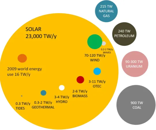
1.1 Diagram of available energy per year for renewable energy sources (Tides, Geothermal, Hydro, Biomass, OTEC, Wind and Solar), total reserve of fossil fuels (Natural Gas, Petroleum, Uranium and Coal), and world needs. 2
1.2 (a) Cost per watt of Silicon photovoltaic cells from 1977 to 2015. (b) Efficiency and cost projections for first- (I), second- (II), and third
generation (III) PV technologies. 3
1.3 Calculated power conversion efficiency limits versus lowest bandgap for the three main photovoltaic solar cell approaches: single junction, tandem (two junctions) and IB. 4
2.1 Valence and conduction band in metals, semiconductors and insulators. 7
2.2 (a) Band diagram for electrons in conduction band and heavy, light and split-off holes in valence band. (b) Fermi-Dirac distribution function
determines electronic occupation in the bands. 8
2.3 Conduction and valence band position for several semi-conductors relative to a common vacuum level, ordered by the electron affinity, . Metals energy is also shown according to their work functions, , 9
2.4 Band-diagram for different types of heterojunctions: type-I (a), type-II (b) and type-III (c). The conduction and valence band edges, EC and EV,
are shown together with the band discontinuities, EC and EV. 10
2.5 Sketch of a tensile strained layer (a) and a compressive strained layer
(b) grown on top of the substrate. 11
2.6 Density of states (g(E)) vs energy for: bulk material (3D) with no confinement, quantum well (2D) with confinement in one direction, nanowire (1D) with carriers confined in two directions, and quantum dots (0D) with carriers confined in the three directions. 12
2.7 Diagram of electron optical recombination (a) and generation (b). 13
2.8 Diagrams of Shockley-Read-Hall (SRH) band-to bound recombination and generation processes. 17
2.9 (a) Cross section of a GaSb quantum ring (QR) embedded in a GaAs matrix. (b) Corresponding band structure of the type-II GaSb/GaAs QR. 19
2.10 (a) Photoluminescence spectra for a GaSb/GaAs nanostructure measured at 4 K under different laser power. (b) Energy of the ground state as a
function of hole population in the QD/QR. 20
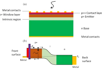
2.11 (a) Solar cell structure based on a p-i-n junction containing a contact layer, window layer, emitter intrinsic region, and base. (b) Band diagram of a solar cell. 22
2.12 Absorption coefficient and penetration depth for Si, GaAs, Ge and
xiv 2.13 Equivalent circuit for a solar cell. 24
2.14 Photovoltaic parameters can be identified identified from I-V curve. 27
2.15 Main loss mechanisms in a single-junction solar cell (SJSC). (a) Band structure of a SJSC showing thermalization and transmission losses. (b)
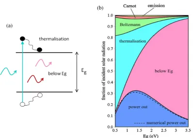
Fraction of incident radiation lost vs bandgap energy. 30
2.16 (a) Band structure of an intermediate band solar cell (IBSC) showing the three energy transitions: (1) VB to CB with energy Eg, (2) VB to
IB with energy EVB-IB, and (3) IB to CB with energy EIB-CB (2). 32
3.1 (a) Bandgap against lattice constant. (b) Spectral irradiance under the AM1.5d solar spectrum for the triple multi-junction cell
InGaP/(In)GaAs/Ge. 34
3.2 Metamorphic growth and wafer bonding have allowed the design
of the four-junction solar cell GaInP/GaAs/GaInAsP/GaInAs. 35
3.3 (a) Sketch of type-I InAs/GaAs high density quantum dot superlattice sandwiched between the p- and n- layers of a GaAs SC. (b)
Corresponding band structure. 36
3.4 InAs/GaAs QD-IBSC with Si doping and the GaAs reference solar cell. (a) Normalized quantum efficiency. (b) J-V curve under 1 Sun. 37
3.5 Reference and type-I InAs/GaAs QDSC 10, 20, 30, 50, 100 and 150 QD layers. (a) Quantum efficiency vs wavelength. (b) I-V curve under
AM1.5g solar spectrum. 38
3.6 J-V curve under AM1.5g solar spectrum for: (a) reference and InAs/GaAs QDSC with 2.1 ML of In coverage and GaP strain balance layer (SBL), 1.8 ML and GaAsP SBL, and 1.8 ML with GaP SBL. (b) Highly dense packed vertically aligned of InGaAs/GaAs QDSC and reference. 39
3.7 Photocurrent extracted from the InAs/AlGaAs QDSC vs wavelength of primary light source at 300 and 20 K. 40
3.8 JL-VOC curves under light concentration up to 1000 suns, for QD-IBSC and GaAs reference cell measured at 150 K (a) and 20 K (b). 41
3.9 Carrier lifetime as a function of delay time, for type-II InAs/GaAs0.82Sb0.18 and type-II InAs/GaAs/GaAs0.82Sb0.18 (blue). (b) Type-I and type-II band alignment for electrons. 43
3.10 Solar cell based with 10 stacked GaSb/GaAs quantum dots and
quantum ring in the intrinsic layer 44
3.11 Reference and GaSb/GaAs QRSC containing 10 and 5 QR stacks. (a) EQE vs wavelength. (b) I-V curve measured under AM1.5g solar spectrum -
experimental data and simulation. 45
3.12 (a) Hole charging and discharging mechanisms in QR: photo-excitation to CB, tunnelling, thermionic emission and photo-excitation to VB. (b)
xv 3.13 Two-photon photocurrent measured for type-II GaSb/GaAs QDSC at 9 K.
(a) EQE vs primary-light wavelength, as intensity of secondary light increases. (b) Ratio of EQE under two photons and under one photon
illumination. 47
3.14 Optical and thermal hole emission rate in GaSb/GaAs QD vs solar
concentration. (b) 300 K open-circuit voltage (Voc) vs solar concentration for GaSb/GaAs QRSC and GaAs SC. 48
4.1 Sketch of MBE growth chamber, showing substrate holder, effusion cells, RHEED gun and screen. 52
4.2 Diagram of Veeco GENxplor MBE System, showing lock chamber pumped by turbomolecular and rotatory pumps, prep-chamber by ion- pump and growth chamber by cryopump. 53
4.3 RHEED specular spot oscillations during layer-by-layer growth of a monolayer: (a) Before growth begins, (b) isolated islands, (c) “completely” assembled layer. 54
4.4 Growth modes: (a) 2D Frank–van der Merwe, (b) 3DVolmer–Weber and (c) 3D Stranski–Krastanov where after wetting layer growth 3D islands nucleate. 55
4.5 (a) and (b) percentage of clusters, rings, and dots for different growth conditions. (c) and (d) AFM images of an uncapped
layers of QD and QR. 56
4.6 (a) Structure of a GaSb/GaAs quantum ring (QR) stack sample. 57
4.7 GaAs reference solar cell with n-doped Base, intrinsic region, p-doped
Emitter, p-doped window layer and p-doped contact layer. 59
4.8 (a) Cross-sectional TEM pictures of five QR layer stack. (b)
Magnification of a single QR. (c) Same as (b) with brighter colours 60
4.9 X-ray diffraction by a plane of atoms spaced a distance d, the incident x- ray reaches the surface with an angle θ. 60
4.10 Photoluminescence set up. 62
4.11 Spider Web Mask, with a diameter of 1.2 mm. 63
4.12 Top contact and Wet etching steps: (1) Spin coating, (2) UV photo- lithography using Top contact mask, (3) developer (4), thermal evaporation of metal contacts, (5) lift off, (6) spin coating, (7) UV photo-litography using Mesa mask, (8) wet etching, and (9) lift off. 64
4.13 The Spider Web Mask pattern: (a) top Contact and (b) mesa. 66
4.14 Diagram of device cross-section after etching the p-i-n junction ~2 μm, isolating each device. 67
xvi 4.16 Solar simulator spectrum normalized to one sun and AM1.5g spectrum. 70
4.17 PVE300 photovoltaic Bentham system. 71
4.18 High light concentration setup at Instituto de Energia Solar (UPM). 72
4.19 Hydrostatic pressure setup at Advanced Technology Institute (Surrey). 73
5.1 (a) Schematic diagram of the GaSb layers within the intrinsic region for: A-(10x 40nm), B-(40x 10nm) and C-(10x 6nm). (b) Sketch of the band structure for device A-(10x 40nm). 79
5.2 p-i-n GaAs SC containing an AlGaAs window layer. (a) Band structure simulation. (b) Device structure. Doping concentration vs depletion
region, showing background doping (c) and depletion width (d). 80
5.3 Cross-section TEM along growth direction, for device B-(40x, 10nm). (a) Bright field and (b) Dark field 002 imaging conditions. 81
5.4 (a)-(c) High resolution XRD for device A-(10x 40nm) & B-(40x, 10nm), showing their corresponding fitting curve. (d) 4 K photoluminescence for: 50 and 10 QR layers spaced 10 nm, and 1 QR layer. 82
5.5 Reference, device A-(10x 40nm) and device B-(40x, 10nm). (a) 300 K EQE. (b) 300 K EQE (log scale). (c) J-V curve under AM1.5g
illumination. (d) 10 K electroluminescence. 84
5.6 (a) –(b) High resolution XRD for device A-XDM563 (10x, 40nm) & C-XDM571 (10x, 6nm) and their correspondent fitting curve. (c)-(d) Cross-section TEM of device C-XDM571(10x, 6nm), in bright and dark field. 86
5.7 Reference, device A- (10x 40nm) and device C- (10x, 6nm). (a) 300K EQE (b) 300 K EQE (log scale). (c) 300 K J-V curve under AM1.5g
illumination. (d) 10 K electroluminescence. 88
6.1 Sketch of hole QR dynamics. 91
6.2 (a) Optical hole emission current vs photo-filling intensity for QRSC. (b) Decay time of normalized as photo-emission flux density is decreased
gradually. 94
6.3 Arrhenius plot of hole emission rate. 95
6.4 Reference, device A- (10x, 40nm), device B- (40x, 10nm) and device C- (10x, 6nm) under solar concentration at 300 K. (a) JL-VOC and dark J–V curve. (b) VOC vs solar concentration. 97
6.5 (a) Ideality factor vs solar concentration for device: A- (10x, 40nm) and B- (40x, 10nm) & C- (10x, 6nm). (b) Dominant recombination processes in high QR stack density QRSCs (devices B & C) vs concentration. 98
xvii 6.7 Electroluminescence intensity for QR peak vs injection current. (a)
Device A- (10x, 40nm) measured at 30 K. (b) Device B- (40x, 10nm)
measured at 19 K. (c). Device C- (10x, 6nm) measured at 40 K. 103
6.8 (a) 10 K Photoluminescence of 20 QR layers spaced by 6 and 10nm. (b) Time-resolved PL for QR peak for 6 and 10 nm spacing. 106
6.9 (a) Normalized photovoltage vs photon energy under pressure of QRSC. (b) Transition energy vs pressure for GaAs bulk layer, GaSb WL, and QR. (c) Band diagram for QR under 0 and 8 kbar hydrostatic pressure. 108
xviii
List of Tables
3.1 Comparison between ideal SJ, ideal IB and type-I QD. 42
3.2 Comparison between type-I InAs/GaAs QDSC and type-II GaSb/GaAs
QD/QRSC. 49
4.1 Quantum ring stack parameters of photoluminescence samples 1x-XDM364 (1x), 10x-XDM426 (10x,10nm) and 50x-XDM497 (50x,10nm). 76
4.2 Quantum ring stack parameters of photoluminescence samples 40nm-PJC645
(10x,40nm), 10nm-QDM672 (20x,10nm) and 6nm-QDM693 (20x,6nm). 76
4.3 Quantum ring stack parameters of solar devices: A-XDM563 (10x,40nm), B-XDM557 (40x,10nm) and C-XDM571 (10x,6nm). 77
4.4 Quantum ring stack parameters of the solar cell device QRSC-A0503 (10x,40nm). 77
5.1 Photovoltaic parameters for reference SC-XDM518 and A-XDM563 (10x, 40nm) and B-XDM557 (40x, 10nm). 85
5.2 Photovoltaic parameters for reference SC and A-XDM563 (10x, 40nm)
and C-XDM571 (10x, 6nm). 89
6.1 Fitting parameters used in eq. 6.4 for the simulation of the photocurrent plot in Figure 6.2(a) measured at 17 K. 94
6.2 Ideality factor for reference, device A, device B and device C, obtained from JL-VOC plot under different concentration ranges 98
6.3 Slope between electroluminescence intensity vs injection current (m) and ideality factor (n). 104
6.4 QR radiative and non-radiative recombination lifetime and emission rates for
photoluminescence samples 40nm, 10nm and 6nm. 106
6.5 Open-circuit voltage relative increase with pressure and temperature for QR SC-A0503 (10x,40nm) and GaAs SC-A0502. 109
1
Chapter 1
Introduction
The development of society depends on access to electricity, for which the demand
increases every year. From 2009 to 2017 human needs increased by 15%, reaching
almost 19 TW/year [1, 2], and by 2050 it is expected to rise up to 27 TW/year
(assuming linear growth). However, today we still depend mostly on fossil fuels, but
reserves are limited and we need to develop alternative renewable energy sources. Solar
energy has a great potential, since 1kW of energy falls on 1 m2 surface perpendicular to
the Sun’s rays on a clear day at sea level. If we were able to collect the sun´s energy
falling on all available land (~ 150 Mkm2 [3]) we could obtain 23,000 TW/year, which
is much larger than expected human needs for 2050. Figure 1.1 compares the available
energy from renewable (TW/year), fossil fuels (TW in total reserve) and the world
energy needs in 2009 (16 TW). Clearly, solar energy shows the highest potential among
the different renewable energies. Even when considering the limitations of land
installation/transportation ( [4, 5]) and photovoltaic panels with an efficiency of 20%,
the one-year solar potential would be of the order of the planetary reserves of coal. A
multiple-year outlook unquestionably shows that if it could be successfully
implemented, solar is the overwhelming energy solution for the future of the planet [6].
Also, solar energy is the only energy source suitable for isolated and remote (off-grid)
areas, as well as in urban areas and in space.
Currently, the solar market is dominated by silicon solar cells with an efficiency of
~27% (mono-crystalline cell) under concentration [7], although many installations are
significantly less than this. Meanwhile, GaAs based solar cells have achieved
2 limited by a maximum efficiency of 31%, reaching 41% under maximum solar
[image:21.595.192.463.112.339.2]concentration of 46,500 suns [8].
Figure 1.1. The diagram shows the available energy in TW per year for the different renewable energy sources (Tides, Geothermal, Hydro, Biomass, OTEC, Wind and Solar), and the energy available in the total reserve of fossil fuels (Natural Gas, Petroleum, Uranium and Coal). Solar energy is the one with the largest availability of 23,000 TW/year (yellow) where the world needs are just 16 TW/ year (orange).
The so-called first generation SJSC is based on thick devices, using a large amount of
semiconductor material, increasing the cost of the final device. Over the last decades the
cost per watt of Silicon panels has decreased dramatically, from 76 to 0.30 $/watt
between 1977 and 2015, as shown in Figure 1.2(a). Figure 1.2(b) shows how in the
second (II) and third (III) generation solar cells the price per solar panel is reduced
compared with the first generation (I). The second generation consists of thin film
technology, based on CdS, a-Si, CuInSe2, CdTe or CIGS, the latter achieving an
efficiency of 22.9% [9]. However, the second generation is also limited by the SJSC
efficiency limit. The third generation involves different approaches to achieve high
efficiency surpassing the SJSC limit, but still limited by the thermodynamic limit of
87% under maximum concentration. The most well-known among all of the approaches
3 achieved an efficiency of 46% [10]. Other emergent concepts exploit multiple e-h pairs,
hot carriers, multiband absorption and thermo-photovoltaics [11].
The SJSC efficiency limit is a consequence of the mismatch between the relatively
narrow spectral absorption of the semiconductor and the broad band solar spectrum. The
light absorption in a semiconductor is limited by its bandgap, such that photons with
energy much larger than the bandgap lose energy via carrier thermalization, and photons
with energy lower than the bandgap are lost by transmission.
Figure 1.2. (a) Cost ($) per watt of Silicon photovoltaic cells from 1977 to 2015, the price has dropped from 76 to 0.30 $/watt [12]. (b) Efficiency and cost projections for first- (I), second- (II), and third generation (III) PV technologies (Si-based, thin-films, and advanced thin-films, respectively) [13].
In a MJSC, two (or more) cells with different bandgaps are stacked on top of each other,
so that each cell absorbs a different part of the solar spectrum, improving sunlight
absorption. Theoretically, in the ideal case of infinite junctions, with individual cells
operating independently, the maximum achievable efficiency is 87%. In this case,
thermalization and transmission losses are suppressed, and the efficiency is determined
just by the thermodynamic limit (see Background Theory chapter section 2.4.3). However, in a MJSC the multiple cells are connected in series, and each of them must
be carefully designed to produce the same current within ~5%, if not the cells start
consuming power instead of generating it. Also, series connection between consecutive
4 specific requirements for developing MJSCs make this approach expensive so that they
are currently limited to use in large scale concentrator systems. [14]
An attractive alternative to MJSC is the intermediate band solar cell (IBSC), which is a
particular case of the multiband approach. The principle for high efficiency is similar to
that in the MJSC, splitting up the spectral absorption to reduce thermalization and
transmission losses to surpass the SJSC efficiency limit. An IBSC consists of a SJSC
with a narrow band in the middle of the bandgap, which enables two extra optical
absorption transitions – valence band to intermediate band (VB-IB) and intermediate
band to conduction band (IB-CB) – which can generate additional photocurrent without
reducing the output voltage (see section 2.5 in Background Theory chapter). Figure 1.3 compares the maximum theoretical efficiency for an IBSC, a two-junction (tandem)
solar cell, and a SJSC (single gap) calculated by Luque et. al [15]. The IBSC exhibits
the highest efficiency of 63%, for a bandgap of 1.93 eV and an energy difference
between CB and IB of 0.7 eV (εi). It is more than 20% higher than the SJSC, without
implementing tunnel junctions or requiring a tandem structure.
Figure 1.3. Calculated power conversion efficiency limits as a function of the lowest band gap for the three main photovoltaic solar cell approaches: single junction, tandem (two junctions) and IB – adapted from [15].
The most common system used to implement IBSC is the quantum dot solar cell
(QDSC), more specifically type-I QDSC, where quantum dots are inserted within a
5 single junction solar cell [16]. However, type-I In(Ga)As/GaAs QDSC have so far
failed to achieve high efficiency for the following reasons. Firstly, QD energy levels are
thermally coupled to the CB, and thermionic emission dominates over optical
generation for pumping photogenerated electrons from IB to CB, limiting the
photocurrent obtained from the IB [17]. Secondly, the short carrier lifetime in type-I QD
reduces output voltage due to the large QD recombination rate [18]. Consequently,
type-II QDSC and type-II quantum ring solar cell (QRSC) have been proposed to
overcome both of these difficulties [19, 20], offering improved IB performance by
reducing the carrier thermal escape rate and enlarging the QD carrier lifetime. However,
high efficiency has not yet been achieved with this approach [21].
This thesis studies the potential improvements to type-II GaSb/GaAs QRSC by (i)
increasing poor sub-bandgap absorption, and (ii) improving low short-circuit current
and open-circuit voltage. The focus is on understanding the main limitations for
implementing IBSC with type-II GaSb/GaAs QRSC, by quantifying all the processes
involved in QR carrier dynamics. Chapter 1 has motivated and introduced the topic of
the thesis. Chapter 2 introduces the background theory required to understand the
results. Chapter 3 reviews the main achievements reported in the literature concerning
the third generation of photovoltaic. Chapter 4 describes the experimental techniques
used in this research. Chapter 5 and 6 present all the experimental and theoretical
6
Chapter 2
Background theory
2.1 Band structure of semiconductors
The properties of solids are conventionally described using band theory which
successfully accounts for the differences between metals, insulators and
semiconductors. The two main bands in a material are the (filled) valence band and the
(empty) conduction band, the difference in energy between them (the bandgap)
determines the electrical conductivity of the material. Figure 2.1 exhibits the energy
distribution of the two bands in metals, semiconductors and insulators. In metals both
bands overlap resulting in very high conductivity (103 – 1010 -1cm-1) as electrons can
move freely in the unfilled band. However, in semiconductors the conduction and
valence band are separated by a small (~1 eV) bandgap, so that electrons can be
thermally excited to the conduction band producing conductivities between 10-12 – 103
-1
cm-1. And, in the case of insulators the bandgap is so large (~5 eV) that electrons
cannot reach the conduction band, resulting in negligible conductivity (<10-12 -1cm-1).
[22]
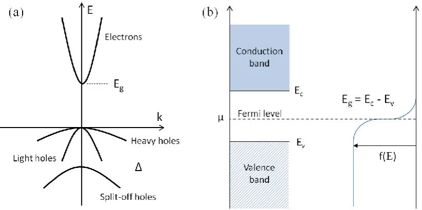
Figure 2.2(a) shows a simplified band a diagram near the Gamma point (k = 0) for semiconductors, showing conduction band and the three bands of valence band: heavy
holes (HH), light holes (LH), and split-off holes (SOH). The energy of each band in
k-space is given by,
(2.1)
7
(2.3)
where are the energy of the conduction band, heavy holes,
light holes and spin orbit holes, respectively; are the corresponding effective masses for each band, h is the Planck constant, k the momentum and the spin orbit splitting.
Figure 2.1. Valence band (blue rectangles) and conduction band (white rectangles) in metals, semiconductors and insulators.
The intrinsic carrier concentration in a semiconductor is controlled by / T, the ratio
of the energy bandgap and the temperature. Assuming parabolic bands the number of
electrons excited to the conduction band at temperature T is given by the Fermi-Dirac distribution integrated up in energy,
(2.4) where is the Fermi energy or chemical potential and is the Boltzmann constant.
Figure 2.2(b) shows the Fermi distribution function for the case of T<< . As the
temperature increases the electrons from valence band are thermally excited to
conduction band, and under bias both the excited electrons in the conduction band and
8 Figure 2.2. (a) Band diagram for electrons (CB) and heavy, light and split-off holes (VB). The difference in energy between the minima of the conduction band (EC) and the maxima of the valence band (EV) is the bandgap energy, EG. And, the energy difference between the maxima of heavy holes and split-off holes is the spin orbit, . (b) Electronic occupation of conduction and valence band determined by Fermi-Dirac distribution function as a function of energy, ( ), for
T<< EG. The Fermi level (μ) lies in the middle of conduction and valence band.
2.1.1 Temperature dependence of bandgap
When the temperature is increased the bandgap energy is reduced, as the separation
between conduction and valence band is shrunk in k space. The two main causes are,
the dilation of the crystal lattice due to thermal expansion of the material [23] and the
interaction between electrons and the quantized lattice vibrations, the phonons [24].
There are different semi-empirical and empirical models for explaining the bandgap
shift with temperature (T), the most common is the Varshni equation [25],
(2.5) where is the bandgap at 0 K, and and are constants that depend on the material,
for GaAs = 2.41x10⁻⁴ eV/K and and = 204 K.
2.1.2 Heterostructure band alignment
Heterojunctions are junctions between two different materials, defined by their bandgap
and electron affinity, . The conduction and valence band discontinuities between
9
(2.6)
(2.7)
Where and are the electron affinities, and and the bandgaps of material 1
and 2, respectively. The electron affinity is the amount of energy necessary to remove
an electron from the conduction band of a semiconductor, in metals the work function
(Φ) is the required energy to extract an electron to the vacuum energy level. Figure 2.3 shows the position of and for the main semiconductors depending on their , also
showing the work function for some metals.
There are three types of band discontinuity determined by the band alignment in the
heterostructure as shown in Figure 2.4: (a) type-I, (b) type-II, and (c) type-III. In type-I, ΔEC is positive and ΔEV is negative, having a conduction band offset (CBO) and a
valence band offset (VBO). In a type-I structure like AlGaAs/GaAs/AlGaAs, electrons
and holes are confined in the lowest bandgap material (GaAs), as shown in Figure
2.4(a). Type-I structures present large light absorption and short carrier lifetime.
Examples of type-I are InAs(Ga,Al)/GaAs and AlGaAs/GaAs.
Figure 2.3. Conduction and valence band position for several semiconductors relative to a common vacuum level at E = 0 eV, taking into account the electron affinity of each semiconductor, . In the right, the work functions for different metals, , are shown for comparison.
In type-II there are two possibilities, ΔEC and ΔEV are positive as shown in Figure 2.4(b)
[image:28.595.243.408.482.643.2]10 sandwiched with GaSb layers with a conduction band offset. Also, ΔEC and ΔEV can be
negative if we consider the inverse structure, where the holes will be confined in the
GaSb layers in GaAs/GaSb/GaAs structure with a valence band offset. Due to low
wavefunction overlap in this structure absorption is inhibited and carrier lifetime is
enhanced. Examples of type-II are GaSb/GaAs and InAsSb/InAs. In type-III the bandgap is broken, allowing electrons to move freely from the valence band of one
material to the conduction band of the other material, for example from GaSb to InAs as
shown in Figure 2.4(c).
Figure 2.4. Sketches of the band-diagram structure for the three types of heterojunctions: type-I (a), type-II (b) and type-III (c). The conduction and valence band edges, EC and EV, are shown together with the band discontinuities, EC and EV.
2.1.3 Strained layers
When growing an epitaxial layer with a lattice parameter ( ) different than the substrate ( ) the lattice mismatch between the two materials is given by
. When the strain between the two materials is too large and above the critical thickness defects and dislocations are generated due to the
relaxation of the top layer [26]. For the elastic strain can be accommodated in the layer growth without degrading the crystal quality of the structure. Depending on
the sign of the layer grown on top of the substrate is tensile strained (positive) or
compressive strained (negative), as sketched in Figure 2.5(a) and 2.5(b). Lattice
matched heterostructures ) give the best device performance due to low dislocation density. Strain induces changes in the band structure like shifting upwards
11
Figure 2.5.Sketch of a tensile strained layer (a) and a compressive strained layer (b) grown on top of the substrate. The rectangle in the bottom represents the substrate with 3x6 unit cells, and on the top is the strained layer with 1x6 unit cells.
2.1.4 Quantum structures
As discussed in section 2.1.2, carriers can be confined in type-I or type-II structures.
When the size of the confinement is similar to the de Broglie wavelength, λB = h / p (h
is Planck’s constant and p the particle’s momentum), the energy level distribution is discrete. The confined energy levels of the particle are obtained by solving the time
independent Schrödinger equation:
(2.8)
where and are the energy and mass of the particle, the particle’s wavefunction
and the potential function.
In a quantum well (QW), the particles are confined just across the z direction.
Considering the well as an infinite potential of length L, the energy of the nth energy level obtained by solving eq. 2.8 is given by
(2.9)
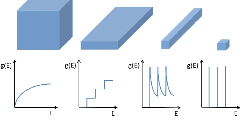
In a quantum dot (QD) the confinement is in the three directions, and the energy levels
are given by eq. 2.9 for each direction x, y and z (Lx, Ly and Lz). The carriers occupy the
energy levels following the density of states (DOS), g(E). The density of carriers per unit energy and unit of volume, N(E), within an energy interval dE is given by [28]
12 Figure 2.6 shows the DOS for the different degrees of confinement. In a bulk material,
there is no confinement in any direction (3D) and DOS is a continuous parabolic
function with energy. In quantum wells, when there is confinement just in one direction
(2D), the DOS follows the step function. For confinement in two directions (1D),
nanowires, the DOS is given by the peak function and, in the case of confinement in all
[image:31.595.120.537.227.434.2]directions (0D), quantum dots, DOS is determined by the Dirac delta function. [29]
Figure 2.6. Density of states (g(E)) vs energy for the different dimensionalities, having different degree of confinement. In a bulk material (3D-blue), there is no confinement in any direction. In a quantum well (2D-red), the confinement is just along one direction. In a nanowire (1D-green), carriers are confined in two directions, and in a quantum dots (0D-yellow), carriers are confined in the three directions.
The occupation of the energy levels is given by the Fermi-Dirac distribution, described
in section 2.1, where the Fermi level lies on the middle of the bandgap in an intrinsic
semiconductor. At 0 K electrons will first fill the energy levels with lower energy, and
then they will distribute following Pauli’s exclusion principle. As the temperature
increases, electrons start populating the conduction band, leaving holes in the valence
band. By multiplying DOS and Fermi-Dirac distribution it is possible to calculate the
13
2.2 Generation and recombination
An electron hole pair (EHP), i.e. an electron in the conduction band and a hole in the
valence band, can be generated or recombined through different band-to-band
processes, radiative and Auger generation/recombination. An EHP can be generated or
recombined radiatively by absorbing or emitting a photon. Also, an EHP can be created
or annihilated via Auger absorbing the energy released by the relaxation of a carrier to a
lower energy state or the inverse process, the EHP recombines transferring the energy of
the transition to a third carrier. An EHP can also be produced or destroyed via
band-to-bound processes, where an electron or hole is generated or recombined via energy levels
in the middle of the bandgap via Shockley-Read-Hall procesess, and via extra energy
levels within the bandgap created close to an interface in heterojunctions or close to the
surface via surface recombination. The generated EHPs increase the carrier
concentration in the semiconductor, producing photocurrent in the device if the carriers
are extracted before they recombine.
2.2.1 Radiative recombination
When an EHP is recombined optically a photon is emitted with an energy equal to the
bandgap. In the inverse process, an EHP is generated by absorbing a photon with energy
equal to or larger than the bandgap. These two processes are sketched in Figure 2.7.
14 Radiative recombination
In equilibrium conditions, without any external stimuli, the law of mass action states
that the product of the hole and electron population is a constant:
(2.11) where ni is the intrinsic carrier concentration, and n0 and p0 are the electron and hole
concentration in equilibrium.
By absorbing light or by injecting current, extra carriers are generated in the
semiconductor, and the population of electrons and holes is modified:
(2.12)
where Δn and Δp are the excess electron and hole population, respectively.
In semiconductors, the recombination rate of the different mechanisms is fundamental
to quantify each process, and to obtain the dominant and limiting recombination
process. The rate at which the carrier concentration decreases (R), corresponding to electrons in the conduction band and holes in the valence band, is proportional to the
hole and electron population,
(2.13) This equation is the so-called bimolecular rate equation, and B is the bimolecular recombination coefficient ~ 10-11 – 10-9 cm3/s for direct-bandgap III-V semiconductors.
[30]
Radiative recombination lifetime for low-level excitation
The recombination dynamics with time are essential to understand the behaviour of
carriers during time-dependent measurements. Since electrons and holes annihilate each
other in a recombination process, then
(2.14)
Using the Bimolecular rate equation to describe the increase in electron and hole
15 (2.15)
For low-level excitation, Δn << (n0 + p0), and by applying eq. 2.14 in eq. 2.15, we have
(2.16)
where R0 and Rexcess are the equilibrium and the excess recombination rates,
respectively.
The time-dependent carrier concentration is given by
(2.17) Where, G0 and R0 are the generation and recombination rates in equilibrium,
respectively.
Now, we obtain the change in electron population after turning off the external stimuli
(light or injected current) where, and using R0 = G0 we have,
(2.18) The solution of this differential equation is,
(2.19)
where, is the carrier lifetime for a radiative process under low-level excitation.
In the case of a p-type semiconductor n0 + p0 ≈ p0 = NA, and the carrier lifetime of eq.
2.19 reduces to
(2.20) where NA is the acceptor density. Similarly, in a n-type semiconductor n0 + p0 ≈ n0 =
ND, the carrier lifetime reduces to
(2.21) where ND is the donor density.
16
(2.22) and the solution is given by
(2.23) Obtaining a time-constant for a non-exponential decay of
(2.24) For long enough time tends to .
2.2.2 Auger recombination
In an Auger recombination process, the energy released from the recombination of the
EHP is transferred to a free carrier, exciting the electron or hole to a higher energy band.
In the inverse process an EHP is generated via an Auger generation process, when
absorbing the energy transferred from a free carrier relaxing to a lower energy band.
The Auger coefficient is large in narrow bandgap materials and decreases with
increasing bandgap, being negligible in wide bandgap materials. [31]
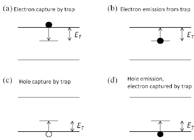
2.2.3 Shockley-Read-Hall recombination
The above processes are band-to-band, where an electron in the conduction band
recombines directly with a hole in the valence band. However, band-to-bound
generation and recombination also occur in semiconductors containing unintentional
impurities or defects producing deep levels in the middle the bandgap which act as
non-radiative recombination centres. These processes are called Shockley-Read-Hall (SRH).
There are four different SRH processes, where electrons and holes can be trapped by
deep centres and/or reemitted from deep centres as shown in Figure 2.9. EHP
band-to-bound recombination occurs in two steps, combining processes (a) and (c) from Figure
2.8, a free electron in the conduction band is first trapped in the deep centre and later
re-emitted to the valence band where it recombines with a free hole. Or inversely, an EHP
17 is trapped by the deep centre from the VB (leaving a hole in its place) and later
reemitted to the conduction band. SRH contribution to EHP generation/recombination
decreases with increasing temperature, as the carrier’s thermal energy increases and
carriers escape to the conduction or valence band. In high carrier injection conditions,
traps are saturated and SRH processes are eventually saturated.
Figure 2.8. Diagrams of Shockley-Read-Hall (SRH) band-to bound recombination and generation processes. An electron from the conduction band can be trapped by a deep centre (a), or be emitted from a deep centre to the conduction band (b). A hole in the valence band can be trapped by a deep centre (c), or be emitted back to the valence band.
The non-radiative recombination carrier lifetime depends on the energy ET and the
concentration NT of the deep level trap. Taking into account that SRH is limited by the
capture of minority carriers, meaning that capture of a majority carrier is more likely,
then the lifetime is given by [32]
(2.25) where and , with and the thermal velocity
and the capture cross-section of the traps of holes and electrons, respectively.
and
[image:36.595.168.488.194.426.2]
18 Fermi level is located at the trap level. For small deviations of equilibrium conditions,
Δn << p0, eq. 2.25 simplifies to
. (2.26) In a semiconductor the total carrier lifetime, τ, includes both the radiative, τr, and
non-radiative, τnr, carrier lifetimes,
(2.27) so that the probability of radiative recombination or more usefully, internal quantum
efficiency is given by
(2.28)
2.2.4 Surface recombination
On the surface of a semiconductor, the lack of crystal periodicity of the lattice and the
unbounded valence orbitals generating partially filled electron orbitals at the surface
(dangling bonds), create electronic states inside the forbidden bandgap. The extra states
acts as non-radiative recombination centres. The minority carrier concentration at the
surface for a p-type semiconductor under illumination is given by
(2.29) where x=0 denotes the surface and x=∞ the bulk, S is the surface recombination velocity, and Ln the electron diffusion length. For large values of S, the minority carrier
concentration at the surface is similar to the equilibrium values. GaAs has particularly
high values for S (106 cm/s) compared with InP (103 cm/s) and Si (101 cm/s).
2.3 Type-II GaSb/GaAs Quantum Ring (QR)
The self-assembled type-II GaSb/GaAs nanostructures can be QD or quantum rings
19 the centre of the QD resulting in a ring shape of GaSb atoms surrounded by GaAs
atoms. By tuning the growth parameters QR can be grown preferentially. A quantum
ring accumulates less strain than a QD due to a decreased volume of the nanostructure
resulting in higher crystal quality, also as shown in Figure 2.9 electrons stay in the
centre hole of the ring (GaAs) as well as in its close surrounding (GaAs) in a QR
increasing optical absorption compared with a QD as explained in Literature review chapter section 3.2.2. The electrons in the conduction band are attracted by Coulomb
force to the holes strongly confined due to the large VB offset between GaAs and GaSb
(~0.5 eV) [33].
Figure 2.9. (a) Cross section of a GaSb quantum ring (QR) embedded in a GaAs matrix. Holes (white circles) are trapped inside the ring while electrons (black circles) are attracted by them, staying in the centre hole of the ring and in its close surroundings. (b) Corresponding band structure of the type-II GaSb/GaAs QR, showing only the ground state energy level. Wetting layer has been ignored for simplicity.
2.3.1 Charging mechanism in type-II GaSb/GaAs quantum rings
In addition to radiative and non-radiative generation and recombination processes, it is
also important to quantify the charging effects in nanostructures. From
photoluminescence (PL) emission the main charging mechanisms can be identified.
Band bending typically has the major contribution, however capacitive charging also
has to be considered. In Figure 2.10(a) the PL spectra of type-II GaSb/GaAs QR
measured by Young et. al. is shown, containing sub-peaks attributed to different hole
20 contribution of band bending and capacitive charging in this structure, revealing that the
capacitive charging effect is stronger [34]. From Figure 2.10(b) the experimental value
for capacitive energy per hole is obtained as 24 ± 2 meV. This value is in agreement
with theoretical calculations, based on
(2.30)
where d is the Böhr diameter (10 nm for GaAs), e the electron charge, A the area of the nanostructure (7.5 and 12.5 nm for inner and outer diameter), the absolute
permittivity, and the relative permittivity (12.9 for GaAs). The theoretical capacitive
energy for a hole inside the GaSb QR is 22 meV, in agreement with the experimental
value.
Figure 2.10. (a) Photoluminescence spectra for a GaSb/GaAs nanostructure measured at 4 K under different laser power. From red to blue the laser power is increased blueshifting the energy of the emission. The sub-peaks correspond to different hole population inside the GaSb nanostructure (from 2 to 8). [34] (b) Energy of the ground state (E0) as a function of hole population in the QD/QR (nh), the experimental data (black dots) fits to a line (red line) with a slope of 24 ± 2 meV. [35]
2.4 Solar Cell (SC)
The solar cells considered in this work essentially consist of a p-n junction producing
electrical current and voltage under illumination. A n junction is formed between a
p-type material with a acceptor concentration NA and n-type material with a donor
21 electrons are ionized and the electron concentration (n) is equal to ND , and all holes are
also ionized with a hole concentration (p) equal to NA. The Fermi levels of each region
before forming a junction are:
(2.31)
where is the potential corresponding to the intrinsic semiconductor ( = )
before adding doping. The output voltage or built in voltage ( ) obtained from a p-n junction is the difference between the Fermi levels of electrons and holes,
, limited by the bandgap of the material.
A solar cell is based on a p-n junction, and a broad response is required which is well
matched to the solar spectrum, optimizing absorption and carrier extraction. The simple
p-n junction can be improved to obtain high efficiency solar cells. Figure 2.11(a) shows
a typical solar cell structure consisting of: a highly doped thin contact layer to reduce
contact resistance at the front, a wide band gap highly doped window layer to avoid
surface recombination without blocking incident light, a thin highly doped emitter to
absorb high energy photons, an intrinsic region to separate n-region from p-region, a
thick low doped base to absorb low energy photons, and a back surface field (BSF) to
avoid surface recombination at the rear. The window layer and BSF are required for
blocking carriers close to the contacts avoiding minority carrier recombination. The
metal contact pattern is optimized for transmitting the maximum sunlight to the material
while collecting the maximum photocurrent, for which finger patterns are the most
commonly used. Figure 2.11(b) shows the p-i-n structure of the solar cells studied in
this thesis including a contact and window layer. The window layer reflects
photogenerated electrons in the emitter so that electrons migrate to the n-region
22 Figure 2.11. (a) Solar cell device based on a p-i-n junction including contact layer, window layer, emitter (p-region), intrinsic region and base (n-region). (b) Band diagram of the corresponding solar cell structure.
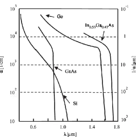
Due to high absorption close to the surface in GaAs (Figure 2.12) it is extremely
important to add a p-AlGaAs layer in the front of the device to prevent high surface
recombination. By adding the AlGaAs layer S is typically reduced from 106 to 104 cm/s. Also, the wide bandgap of AlGaAs transmits most of the light through to the p-GaAs
layer. In GaAs the electron diffusion length is higher than that for holes (for the same
doping level in GaAs) making p-n junctions more suitable for solar cells than n-p
junctions, such that electrons reach the n-contact across the thick p-region before
recombining. In addition, high doping in the window layer gives low contact resistance
so that the p-GaAs layer can be lightly doped increasing carrier lifetime and
[image:41.595.124.546.52.339.2]23 Figure 2.12. Absorption coefficient (α) and penetration depth (1/ α) for Si, GaAs, Ge and InGaAs. Showing high energy photons absorbed close to the surface. GaAs has an absorption coefficient around one order of magnitude higher than Si, making more suitable for solar cell applications. [36]
2.4.1 Junction capacitance
Determining the intrinsic carrier concentration in solar cells is crucial to control the
un-intentional impurities in the lattice improving the crystal quality of the material. By
measuring the capacitance vs voltage characteristic, depletion width (W), built-in voltage (Vbi) , acceptor concentration (NA) and intrinsic carrier concentration (ni) can be
obtained. The capacitance across the junction with an area A is given by
(2.32)
Assuming an abrupt junction between the n-region and p-region, W depends on the applied voltage ( ) and is given by
(2.33)
In the case that one side of the junction is more heavily doped than the other one, eq.
2.33 is simplified. Applying the condition NA >> ND, the square of the inverse of the
capacitance becomes
[image:42.595.209.435.56.284.2]24 obtaining from the slope and from the intercept on the voltage axis from the plot of 1/C2 as a function of Va. By substituting the two values in eq. 2.34, W is obtained at a
certain bias. Alternatively, by plotting ND as a function on W can be obtained from the intercept while ND corresponds to ni for W<< Wgrown (Wgrown is the i-region thickness
in a p-i-n structure).
2.4.2 Photovoltaic performance
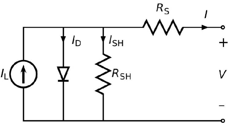
The equivalent circuit corresponding to a real solar cell is sketched in Figure 2.13,
consisting of a diode producing a dark or saturation current ID plus a current source
generating a photocurrent, IL under illumination, and to account for current and voltage
losses series and shunt resistance are included. Series resistance (RS) includes contact
resistance and recombination within the material structure, while shunt resistance (RSH)
accounts for leakage current across the sidewalls of the device due to surface
recombination. Both can be reduced by improving crystal quality in the material, by
optimizing grid design, and by performing edge passivation. In solar cells generally
series resistance has a stronger effect compared with shunt resistance on photovoltaic
[image:43.595.141.513.496.696.2]performance.