© 2016, IRJET ISO 9001:2008 Certified Journal
Page 927
SIMO Boost Converter to Obtain Simultaneous AC and DC Output
Syed Meeran M
1, Prabakaran D
2, Parthasarathy C
3Prasanth S
41
Assistant Professor, Department of Electrical and Electronics Engineering, M.A.M. School of Engineering
2,3,4UG Scholars, Department of Electrical and Electronics Engineering, M.A.M. School of Engineering
---***---Abstract -
This paper presents a novel technique to obtainsimultaneous multi stage boost AC and DC output with a single stage input. A single input is applied at the input side of the boost converter and multi state output is obtained. To achieve minimum switching loss, only one power stage works at a high frequency is called as Boost to Boost mode of operation. An Inductor is used in the power loop to reduce the conduction losses during operation. The principle of operation is demonstrated through the analysis on the equivalent circuits of a “half-bridge” single-phase inverter. The theoretical analysis shows that when input dc voltage is larger than the magnitude of the ac voltage, it is a voltage-source inverter, and on the contrary it is current-source inverter in the other mode. Simulations and experiments show that it has a good control and system performance.
Key Words: Boost in boost, buck in buck, CL filter, current-source inverter (CSI), efficiency, LCL filter, voltage-source inverter (VSI)
1. INTRODUCTION
Vast usage of renewable energy as a global accepted alternative source urges the use of grid-tied inverters [1]– [3]. The converters can be divided into voltage-source inverters (VSI) and current-source inverters (CSI), where the VSI is the dominant converter. One of the reasons is that the VSI does not need a large inductor as the energy storage element, while the CSI should adopt a larger inductor in order to keep the dc current constant for a proper modulation. The research related to CSI mainly focus on the control [4]–[7]. So far, how to decrease the total dc-link inductance for CSI is a challenge, especially in the low voltage and three-phase application area.
Since the VSI is a step-down inverter and the CSI is a kind of step-up inverter, the Z-source inverters (ZSI) was proposed in [8] in order to fully utilize the basic character of VSI and CSI and the minimum semiconductors were used with the combined characters of the step-down and the step-up converters. How-ever, compared to the CSI or the VSI, the ZSI has two extra inductors in the power loop, which may sacrifice the efficiency [9], [10]. The control difficulty is also a demerit in the Z-source impedance.
In the renewable power generation system, the input dc volt-age of the converter may vary greatly. For example, the output dc voltage of a solar panel will change a lot under
different temperature conditions. To transfer this kind of dc energy into the grid, a two- or three-stage inverter may be required as the power interface, especially for the VSI-based system. If all power stages work at high frequency, the efficiency of the inverter will be in-evitable affected. In order to decrease the switching frequency, many interesting inverters have been proposed [11]–[13] and the basic idea is to ensure that only one of the power stages of the system works at high frequency. Nevertheless, the main output filter of these inverters should be designed to satisfy the harmonic requirements [14] in the “buck” mode, especially when the dc input voltage is higher than the amplitude of the grid voltage. Thus, when they work in the “boost” mode, an over filtering may take place due to that the output filter is a CL– CL filter. Since the excessive inductance is in the power loop, extra conduction losses will be present and the grid current is not easy to control as well.
A consensus has been reached that the power electronics will take a main role in the future energy area [15]. But which favourite type of grid-tied inverters for the future is still discussed. Dependent on the efficiency evaluation, the smaller inductance in the power loop will cause a higher efficiency, due to the fact that the power loss caused by power device has be-come smaller and smaller. Thus, it may be a good way to achieve high efficiency through decreasing the total inductance in the power loop. It should be pointed out that aiming to minimize the inductance of output filter of VSI, a recently new type of power filter named as the LLCL-filter was proposed and analysed for the grid-tied VSI [16]– [18]. Theoretically, compared with an LCL-filter, an LLCL-filter can save the total inductance. Due to the reason of familiarity, the conventional LCL-filter is still used as the output filter benchmark for the comparison between several classical inverters.
© 2016, IRJET ISO 9001:2008 Certified Journal
Page 928
Fig-1: Signle Phase Grid Tied VSIFig-2: Single Phase Grid Tied CSI
Fig-3: Single Phase Grid tied ZSI
2. TYPICAL FULL-BRIDGE SINGLE-PHASE
GRID-TIED CONVERTER WITH THE DIFFERENT
POWER SOURCE
2.1
Single-Stage Converters
1. Inverters with the Single Function of Down or Step-Up: Figs. 1 and 2 show the typical VSI with LCL-filter and the typical CSI with CL-filter, respectively. The VSI is buck-type (step-down) inverter, which means its dc voltage should be higher than the amplitude of the grid voltage. The CSI is a boost-type (step-up) inverter, which means that its dc voltage should be lower than the amplitude of the grid voltage [19]. Generally, the output dc voltage of the renewable power source (for example, a PV panel) may vary in a large range, then the VSIs or the CSIs have their own limitations as a renewable power conditioner connected to the grid directly, and after an additional dc/dc converter is used.
2. Inverters With the Function of Both Down and Step-Up:
a) ZSI: Combined with the voltage characters of the VSI and the CSI, a Z-source type inverter was proposed [8]. In theory, ZSI (as shown in Fig. 3) can work in the step-down and the step-up states as required and its reliability can be improved a lot, owing to its immunity to the electromagnetic interference. However, due to the two additional inductors in the power loop, the conduction power loss is high and over filtering may also take place, especially when the input dc voltage is high. It is basically a boost–buck type converter and it is difficult to realize the overall parameter optimization, when the input dc voltage varies in a large range. The efficiency of the ZSI seems not as high as that of the other conventional two-stage inverters [9], [10].
Fig-4: Single phase grid tied natural soft switching inverter
© 2016, IRJET ISO 9001:2008 Certified Journal
Page 929
2.2
Two-Stage “Boost in Boost, Buck in Buck”
Converter
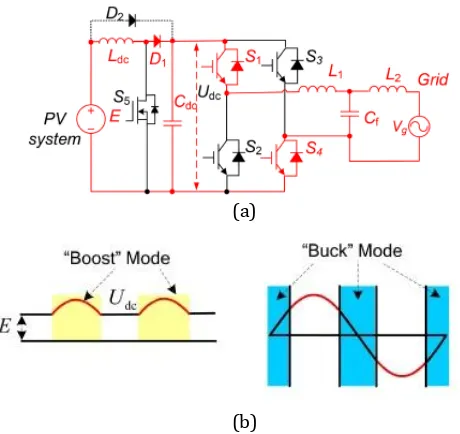
The traditional two-stage VSI adopts an input dc/dc boost converter to transfer a variable input dc voltage into a stable dc voltage, and then injects the dc energy into the grid. So, both two stages of the power converter work at high frequency, causing considerable switching losses. Fig. 5 shows a conventional two stage dual-mode time-sharing high efficiency inverter used as a PV inverter [11]. Here, an LCL-filter is used instead of an L-LCL-filter to reduce the total inductance. The outstanding character of this inverter is that only one power stage is chopping at high frequency at any time, so the switching power losses can be decreased, compared to other conventional two-stage power converter with the constant dc-link voltage. Its character can be summarized as a “boost in boost, buck in buck” converter, which means that the converter works in the “boost” or “buck” state with the high frequency only when the “boost” or the “buck” is needed to minimize the switching losses. Further, in order to reduce the conduction power loss of the dc inductor, a bypass diode D2 is often used [24].
However, during the “boost” working stage, the over filtering still takes place since the equivalent output filter of the “boost” circuit is a CL–CL filter and the extra conduction loss of the inductor cannot be avoided.
(a)
[image:3.595.321.541.356.568.2](b)
Fig -5: Conventional two stages dual-mode time-sharing converter with LCL-filter: (a) topology and (b) operating
principle [11].
3. PROPOSED CONVERTER
3.1Topologies of “Full-Bridge” and “Half-Bridge” converter
A three-stage inverter was adopted in order to achieve higher efficiency with devices of MOSFET. One merit of the
of dc input source is smaller than that of the conventional VSI. Note that due to the energy balance, a large input smoothing capacitor should be inserted and its capacitance is mainly dependent on the ripple current at the double line frequency, so this LC filter has less help to decrease the total input capacitance.
Since the input dc LC-filter of the conventional three-stage dual-mode time-sharing inverter may not be so necessary, a new family “boost in boost” inverter is proposed and abbreviated as the Aalborg Inverter. A “full-bridge” three-stage inverter is proposed and shown in Fig. 6. Similar to the conventional three-stage dual-mode time-sharing inverter, only one power stage works at high frequency and the output power stage works at the line frequency. Compared with the inverter in [13], the main difference is that the physical position of “boost” stage and “buck” stage has been exchanged and one inductor can be saved. So, in theory, the relatedconduction power loss is also reduced and a higher efficiency can be achieved.
(a)
(b)
Fig -6: Proposed “full-bridge” converter: (a) topology and (b) Operating principle.
[image:3.595.39.269.442.659.2]© 2016, IRJET ISO 9001:2008 Certified Journal
Page 930
Fig -7: Proposed Half Bridge converter AFig-8: Proposed Half Bridge converter B
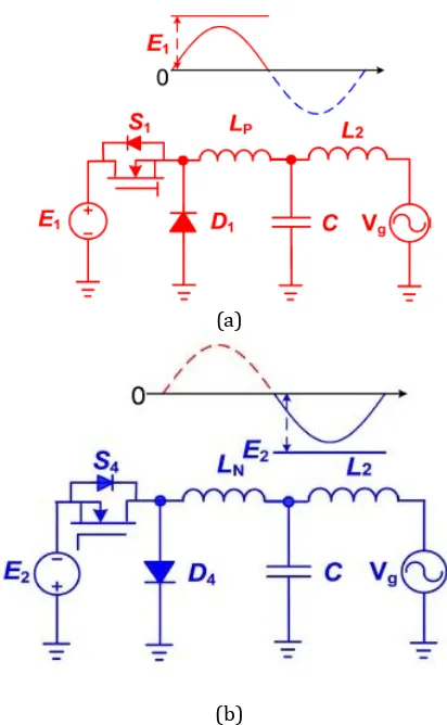
3.2 Operating Modes of the Proposed “Half-Bridge” Inverter-A
1) |E1 | or |E2 | ≥ Vg A : When the input dc voltage (E1 , E2)
is larger than Vg A , the amplitude value of grid voltage,
the equivalent circuits are as shown in Fig. 9. As shown in Fig. 9(a), during the positive period of the grid voltage, S3 is ON, S2 is OFF, S1 works at high
frequency in order to achieve a sinusoidal grid-injected current, and E1 provides the total energy. In
the same way, as shown in Fig. 9(b), during the negative period of Vg , S6 is ON, S5 is OFF, S4 works in
the high frequency mode in order to keep the grid-injected current sinusoidal, and E2 delivers the total
energy. The inverter works as a VSI connected to the grid through an LCL-filter.
2) |E1 | and |E2 | < Vg A: When the input dc voltage (E1 ,
E2) is lower than the amplitude of grid voltage (Vg A ),
the control becomes a little bit more complicated. Fig. 10 shows the working sequence of the proposed “half-bridge” inverter-A, when the amplitude of the input dc voltage is lower than the ac grid voltage, where the sequence can be separated into six parts during a full line frequency period.
(a)
(b)
Fig-9: Equivalent circuits when E1 and E2 are higher than
the amplitude of the grid voltage: a) during positive period, b) during negative period
During T1 and T3, S3 is ON, S1 works at high frequency, and the
rest of the switches are OFF. The equivalent circuits are shown in Fig. 11(a) and it can be seen that it works like a pure buck converter with an LCL-filter connected to the grid. In this case, the buck converter is a classical VSI.
During T2 , S1 and S3 are ON, S2 works with high frequency,
and the rest of the switches are OFF. The equivalent circuit is shown in Fig. 11(b) and it can be seen that it works like a pure boost converter with a CL-filter connected to the grid. If the current of the boost inductor can be fully controlled, this equivalent circuit can be seen as a CSI.
Similarly, during T4 and T6 , S6 is ON, S4 works at high
[image:4.595.328.534.107.441.2]© 2016, IRJET ISO 9001:2008 Certified Journal
Page 931
Fig-10:
Working sequence when E1 and E2 are lower thanthe amplitude of the grid voltage: (a) during the positive period and (b) during the negative period.
Fig-11: Equivalent Circuits during positive period of the converter a) During T1 and T3 b) During T2
During T5 , S4 and S6 are ON, S5 works at high frequency, and
the rest of the switches are OFF. The equivalent circuit is shown in Fig. 12(b) and it can also be seen as a CSI with a CL-filter connected to the grid, if the current of the boost inductor can be fully controlled.
From the previous analysis, it can be seen that the proposed inverter cannot simply be identified as a conventional VSI or CSI. The most outstanding character of this type inverter is that the minimum filtering inductance in the power loop is adopted and over filtering will not take place; so, theoretically, the pro-posed inverter has the merit to achieve higher efficiency than other inverters under the same condition of the input dc voltage.
Fig-12: Equivalent circuits during the negative period for the converter. (a) During T4 and T6. (b) During T5
4. SIMULATIONS AND EXPERIMENTAL
RESULTS
Simulations on the proposed “Half-bridge” Inverter-A as shown in Fig. 7 are carried out with the PSIM software. The parameters are listed in Table I. During the simulation, the delay is considered as 0.75 Ts , and the grid voltage is set to
220 V. The simulation results are shown in Figs. 13–16 respectively.
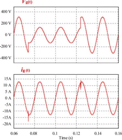
Fig-13: Simulated input dc voltages (E1, E2 ), grid voltage
(Vg (t)), dc currents of dc inductor (iLN (t), iLP (t)), and grid
injected current (ig (t)) while E1 = E2 = 350 V and 2000 W
© 2016, IRJET ISO 9001:2008 Certified Journal
Page 932
Fig. 13 shows the simulation results of the input dc voltages [image:6.595.35.274.188.483.2](E1 , E2 ), the grid voltage (Vg (t)), the dc currents of the dc inductor (iL N (t), iL P (t)), and the grid-injected current (ig (t)) while E1 = E2 = 350 V. It can be seen that the inverter works as a pure VSI and the current of the dc inductor is a rectified sinusoidal waveform, which is set according to (6).
Table 1:Design Parameters of 2 KW Converter
Parameters
L
2C
L
N, L
Pf
s(S
1-S
5)
Units
600 µH
2µF
600 µH
40 kHz
Fig-14: Simulated input dc voltages (E1 , E2 ), grid voltage
(Vg (t)), dc cur-rents of dc inductor (iL N (t), iL P (t)), and
grid-injected current (ig (t)) when E1 = E2 = 240 V and
2000 W operation (full load).
When E1 = E2 = 240 V, the simulated results are shown in
Figs. 14–16. From Fig. 14, it can be seen that when the instantaneously ac grid voltage is higher than the input dc voltage, the boost circuit works quite well according to the proposed control strategy. Fig. 15 shows the simulated voltage Vg(t) and the grid-injected current ig (t) when the
given output power changes from the half load to the full load at the time of 0.084 s, and back to the half load again at 0.124 s. Fig. 16 also shows the simulated voltage Vg (t) and
the grid-injected current ig (t), when a volt-age sag of 50%
appears in the grid voltage between 0.074 and 0.124 s. From Figs. 15 and 16, it can be seen that the converter has good control performance, which is due to the fact that the minimum filtering inductance in the power loop has been used, especially during the “boost” working stage.
Fig-15: Simulated grid voltage (Vg (t)) and grid-injected
current (ig (t)) when the given power changes at 0.084 and
0.124 s (from the half-load to the full load, then back to the half-load).
Fig-16: Simulated grid voltage (Vg (t)) and grid-injected
current (ig (t)) when the grid has a voltage sag between
0.074 and 0.124 s.
5. CONCLUSION
[image:6.595.333.531.367.594.2]© 2016, IRJET ISO 9001:2008 Certified Journal
Page 933
“boost in boost” inverter, only one power stage works in thehigh frequency stage at any time, which results in minimum switching losses. Different from the traditional “boost in boost” inverter, the inverter has a minimum voltage drop of the filtering inductors in the power loop at any time.
REFERENCES
[1]J. W. Kolar, T. Friedli, J. Rodriguez, and P. W. Wheeler, “Review of three-phase PWM ac–ac converter topologies,” IEEE Trans. Ind. Electron., vol.
58, no. 11, pp. 4988–5006, Nov. 2011.
[2] D. Meneses, F. Blaabjerg, O. Garc´ıa, and J. A. Cobos, “Review and com-parison of step-up transformerless topologies for photovoltaic ac-module application,” IEEE Trans. Power Electron., vol. 28, no. 6, pp. 2649–2663, Jun. 2013.
[3] F. Blaabjerg, M. Liserre, and K. Ma, “ Power electronics converters for wind turbine systems,” IEEE Trans. Ind. Appl., vol. 48, no. 2, pp. 708–719, Mar./Apr. 2012. [4] H. J. Lee, S. Jung, and S. K. Sul, “Current controller design
for current source inverter-fed ac machine drive system,” IEEE Trans. Power Elec-tron., vol. 28, no. 3, pp. 1366– 1381, Mar. 2013.
[5] N. Zhu, D. Xu, B. Wu, N. R. Zargari, M. Kazerani, and F. Liu, “Common-mode voltage reduction methods for current-source converters in medium-voltage drives,” IEEE Trans. Power Electron., vol. 28, no. 2, pp. 995–1006, Feb. 2013. [6] Z. Wang, B. Wu, D. Xu, and N. Zargari, “Hybrid PWM for high-power current-source-inverter-fed drives with low switching frequency,” IEEE Trans. Power Electron., vol. 26, no. 6, pp. 1754–1764, Jun. 2011.
[7] R. T. H. Li, H. S. H. Chung, and T. K. M. Chan, “An active modula-tion technique for single-phase grid-connected CSI,” IEEE Trans. Power Electron., vol. 22, no. 4, pp. 1373– 1382, Apr. 2007.
[8] F. Z. Peng, “Z-source inverter,” IEEE Trans. Ind. Appl., vol. 39, no. 2, pp. 504–510, Mar./Apr. 2003.
[9] R. Burkart, J. W. Kolar, and G. Griepentrog, “Comprehensive compar-ative evaluation of single- and multi-stage three-phase power converters for photovoltaic applications,” presented at the IEEE 34th
International Telecommunications Energy Conference,
Scottsdale, AZ, USA, Sep. 30– Oct. 4, 2012.
[10] J. Li, J. Liu, and Z. Liu, “Comparison of Z-source inverter and traditional two-stage boost-buck inverter in grid-tied renewable energy generation,” in Proc. IEEE 6th Int. Power Electron. Motion Control Conf., Wuhan, China, May 17–20, 2009, pp. 1493–1497.
[11] K. Ogura, T. Nishida, E. Hiraki, M. Nakaoka, and S. Nagai, “Time-sharing boost chopper cascaded dual mode single-phase sinewave inverter for solar photovoltaic power generation system,” in Proc. IEEE 35th Annu.
Germany, pp. 4763– 4767.
[12] W. Wu and T. Tang, “Dual mode time-sharing cascaded sinusoidal in-verter,” IEEE Trans. Energy Convers., vol. 22, no. 3, pp. 795–797, Sep. 2007.
[13] Z. Zhao, M. Xu, Q. Chen, J. Lai, and Y. Cho, “Derivation, analysis, and implementation of a boost–buck converter-based high-efficiency PV inverter,” IEEE Trans. Power Electron., vol. 27, no. 3, pp. 1304–1313, Mar. 2012
[14]IEEE Application Guide for IEEE Std. 1547, IEEE Standard for Inter-connecting Distributed Resources With Electric Power Systems, IEEE 1547.2-2008, 2008. [15]B. K. Bose, “Global energy scenario and impact of power
electronics in 21st century,” IEEE Trans. Ind. Electron., vol. 60, no. 7, pp. 2638–2651, Jul. 2013.
[16]W. Wu, Y. He, and F. Blaabjerg, “An LLCL-power filter for single-phase grid-tied inverter,” IEEE Trans. Power Electron., vol. 27, no. 2, pp. 782– 789, Feb. 2012. [17]W. Wu, Y. He, T. Tang, and F. Blaabjerg, “A new design
method for the passive damped LCL- and LLCL-filter based single-phase grid-tied inverter,” IEEE Trans. Ind. Electron., vol. 60, no. 10, pp. 4339–4350, Oct. 2013. [18]W. Wu, Y. Sun, M. Huang, X. Wang, H. Wang, F. Blaabjerg,
M. Liserre, and H. S. H. Chung, “A robust passive damping method for LLCL filter based grid-tied inverters to minimize the effect of grid harmonic voltages,” IEEE Trans. Power Electron., vol. 29, no. 7, pp. 3279–3289, Jul. 2014.
[19]R .O. Caceres and I. Barbi, “A boost dc-ac converter: Analysis, de-sign, and experimentation,” IEEE Trans. Power Electron., vol. 14, no. 1,134–141, Jan. 1999. [20]A. Wintrich, U. Nicolai, W. Tursky, and T. Reimann,
Application Man-ual Power Semiconductors. Nuremberg, Germany: Semikron Int., 2011, 275–279.
[21]W. Wu, B. Gu, Z. M. Qian, and F. Z. Peng, “A natural soft-switch power converter with adjustable dc-link voltage,” in Proc. Chin. Soc. Elect. Eng., vol. 25, 2005, no. 12, pp. 62– 66.
[22]W. Wu, P. Geng, J. Chen, Y. Ye, and T. Tang, “A novel three-phase quasi-soft-switching dc/ac inverter,” in Proc. IEEE Int. Symp. Power Electron. Distrib. Gener. Syst., Hefei, China, Jun. 16–18, 2010, pp. 477–480
[23]P. Geng, W. Wu, and F. Blaabjerg, “Efficiency analysis on a two-level three-phase quasi-soft-switching inverter,” in Proc. Appl. Power Electron. Conf., Long Beach, CA, USA, Mar. 17–21, 2013, pp. 1206–1212.
[24]N. A. Ahmed, H. W. Lee, and M. Nakaoka, “Dual-Mode time-sharing sine wave-modulation soft switching boost full-bridge one-stage power conditioner without electrolytic capacitor dc link,” IEEE Trans. Ind. Appl., vol. 43, no. 3, pp. 805–813, May/Jun. 2007.
© 2016, IRJET ISO 9001:2008 Certified Journal
Page 934
[26]Y. A.-R. I. Mohamed, M. A. Rahman, and R. Seethapathy,“Robust line-voltage sensor less control and synchronization of LCL-filtered distributed generation inverters for high power quality grid connection,” IEEE Trans. Power Electron., vol. 27, no. 1, pp. 87–98, Jan. 2012.
[27]J. He and Y. W. Li, “Generalized closed-loop control schemes with embedded virtual impedances for voltage source converters with LC or LCL filters,” IEEE Trans. Power Electron., vol. 27, no. 4, pp. 1850–1861, Apr. 2012. [28]W. Wu, H. Geng, P. Geng, Y. Ye, and M. Chen, “A novel control method for dual mode time-sharing grid-connected inverter,” in Proc. IEEE Energy Convers. Congr. Expo., Atlanta, GA, USA, Sep. 12–16, 2010, pp. 53–57. [29]J. Mulethaler, M. Schweizer, R. Blattmann, J. W. Kolar,
and A. Ecklebe, “Optimal design of LCL harmonic filters for three-phase PFC rectifiers,” IEEE Trans. Power Electron., vol. 28, no. 7, pp. 3114–3125, Jul. 2013. [30]N. He, D. Xu, Y. Zhu, J. Zhang, G. Shen, Y. Zhang, J. Ma, and
C. Liu, “Weighted average current control in a three-phase grid inverter with an LCL filter,” IEEE Trans. Power Electron., vol. 28, no. 6, pp. 2785–2797, Jun. 2013. [31]X. Bao, F. Zhuo, Y. Tian, and P. Tan, “Simplified feedback
linearization control of three-phase photovoltaic inverter with an LCL filter,” IEEE Trans. Power Electron., vol. 28, no. 6, pp. 2739–2752, Jun. 2013.
[32]X. Hao, X. Yang, T. Liu, L. Huang, and W. Chen, “A sliding-mode con-troller with multiresonant sliding surface for single-phase grid-connected VSI with an LCL filter,” IEEE Trans. Power Electron., vol. 28, no. 5,2259–2268, May 2013.
[33]S. lvaperumal, C. C. A. Rajan, and S. Muralidharan, “Stability and per-formance investigation of a fuzzy-controlled LCL resonant converter in an RTOS environment,” IEEE Trans. Power Electron., vol. 28, no. 4, 1817–1832, Apr. 2013.
[34]W. Wu, Y. Sun, Z. Lin, Y. He, M. Huang, F. Blaabjerg, and H. S.-H. Chung, “A modified LLCL filter with the reduced conducted EMI noise,” IEEE Trans. Power Electron., vol. 29, no. 7, pp. 3393–3402, Jul. 2014.