© 2016, IRJET | Impact Factor value: 4.45 | ISO 9001:2008 Certified Journal | Page 619
Optimal Implementation Of UART_SPI Controller and Slave Interface
With Master.
Asst .Professor Ms. Sneha Nagar and Ms. pratima sharma
Department of Electronics and Communication Engineering, Oriental University, Indore, (MP Indore, (MP)
---Abstract :
This paper details the design and usage for the universal asynchronous receiver/transmitter to serial peripheral interface .The UART-to-SPI interface can be used to communicate to SPI slave devices from a PC with a UART port. SPI is a full duplex, serial bus commonly used in the embedded world because of its simple hardware interface requirements and protocol flexibility. SPI devices are normally smaller in size (IOI/O) count when compared to parallel interface devices. This design example is implemented on an ASIC device, but can easily be implemented in any of low power field programmable gate arrays (FPGAs) to optimize system power, size or performance requirements.Keywords: SOC, UART, SPI, power optimize.
1. Introduction
A UART is usually an individual BClkx8 (or part of an) integrated circuit used for serial communications over a computer or peripheral device serial port. UARTs are now commonly included in microcontrollers. A dual UART or DUART combines twoUARTs into a single chip.Many modern ICs now come with a UART that can also communicate synchronously; these devices are called USARTs(universal synchronousasynchronous receiver/transmitter). An UART is a device allowing
the transmission and reception of information, in a serial and asynchronous way. Universal Asynchronous Receiver and Transmitter are used asynchronous serial data communication between remote embedded systems. The UART can be used to control the process of breaking parallel data from the PC down into serial data that can be transmitted. It consists of one receiver module and transmitter module. UART has been an important input/output tool for decades and is still widely used. UARTs are used for communication between two devices.
[1]. SPI stands for Serial Peripheral Interface. It is a synchronous protocol that allows a master device to initiate
communication with slave devices.
that allows a master device to initiate communication with slave devices.
FIGURE 1 UARTBLOCK DIAGRAM
TX
DONE
SIONA
L
TH
R
TS
R
11
bit-data
Tx
out
Tx
don
e
8
© 2016, IRJET | Impact Factor value: 4.45 | ISO 9001:2008 Certified Journal | Page 620 SPI is a full duplex, serial bus commonly used
because of its simple hardware interface requirements and protocol flexibility. SPI consists of two blocks. The SPI master and the SPI slave, the SPI Master which is being used in this design implements the master functionality of the SPI protocol. SPI protocol specifies four signal wires .
MISO - master out slave in , MISO - master in slave out , SCLK - serial clock and SS - slave select [2].The SPI Master block generates the control signals to interface to external slave devices using the serial data out port (MOSI), serial data in port (MISO), output clock (SCLK) and slave select (SS) [8] .The SS signal mustbe used if more than one slave exists in the system middle block joins the UART and SPI master. It helps the interconnection. middle block joins the UART and SPI master. It helps the interconnection between these two interfaces.
The main advantage is, the UART- SPI interface [7] can fit in any application where an SPI device has to be used without any difficulties. As the UART-SPI interface can be used to communicate to SPI slave devices from a PC with UART port it can be used for typical applications like interfacing of EEPROM, flash memories and sensors [6].
2. System-On-Chip
Moore’s law not only states that their will be increase in density of transistors technology advances. It also inflict new demands and challenges, Complexity of systems also varies at the high rate of speed. As
technology advances still the old architecture proposed 20 years back cannot be adopted, new architectures has to be followed. As per the Moore’s law revolution, in the mid-eighties was the way to embed more and more electronic devices in the same silicon die; it was the era of System on Chip [8]. The main challenge was the way to interconnect all these devices effectively towork efficiently. Because of this need we use Bus interconnect structure for VLSI sub system.
An embedded system usually has an embedded user interface as a form of software and consists many components inside, not only the hardware but also the software that constitutes the system is important. Such a complicated and complex entity can be handled only with computer-aided design tools, automatic synthesis of the physical layouts, and software engineering knowledge. In addition, the system functions to achieve a specific goal, as a whole, are usually described in algorithms that should satisfy user requirements in time.
3. UART Design
© 2016, IRJET | Impact Factor value: 4.45 | ISO 9001:2008 Certified Journal | Page 621 are sent, with the Least Significant Bit(LSB)being sent
first. Each bit in the transmission is transmitted for five to eight data bits, least-significant-bit first, an optional "parity" bit, and then one, one and a half, or two "stop" bits. The start bit is the opposite polarity of the line's idle state. The stop bit is the data-line's idle state, and provides a delay before the next character can start. (This is called asynchronous start-stop transmission). In mechanical teletypes, the "stop" bit was often stretched to two bit times to give the mechanism more time to finish printing a character. A stretched "stop" bit also helps resynchronization. As part of this interface, the UART also [3]:
• Converts the bytes it receives from the system along parallel circuits into a single serial bit stream for outbound transmission
• On inbound transmission, converts the serial bit stream into the bytes that the system handles .
• Adds a parity bit (if it's been selected) on outbound • transmissions and checks the parity of incoming bytes (if selected) and discards the parity bit.
• Wait until the incoming signal becomes ' 0 ' (the start bit) and then start the sampling tick center. When the center reaches 7, the incoming signal reaches the middle position of the start bit. Clear the center and restart.
4. SPI Design
The "Serial Peripheral Interface" (SPI) is a synchronous four wire serial link used to connect microcontrollers to sensors, memory, and peripherals. It's a simple "de facto" standard, not
complicated enough to acquire a standardization body. SPI uses a master/slave configuration. The three signal wires hold a clock (SCK, often on the order of 10 MHz), and parallel data lines with "Master Out, Slave In" (MOSI) or "Master In, Slave Out" (MISO) signals. (Other names are also used.) There are four clocking modes through which data is exchanged; mode-0 and mode-3 are most commonly used. Each clock cycle shifts data out and data in; the clock doesn't cycle except when there is a data bit to shift. Not all data bits are used though; not every protocol uses those full duplex capabilities.
SPI consists of one master device and one or more slave devices. If more than one slave device are connected to the master then Slave Select (SS) signal is used which
Fig no. 2
FIGURE 2:Master Slave interface
SPI consists of one master device and one or more slave devices. If more than one slave device are connected to the master then Slave Select (SS) signal is used which is active low. To begin a communication, the bus master first configures the
Master
Slave
Tx Data Register
SPI Shift Register
Rx Data Register
Rx Data Register Tx Data Register
SPIShift Register
MISO
© 2016, IRJET | Impact Factor value: 4.45 | ISO 9001:2008 Certified Journal | Page 622 clock, using a frequency less than or equal to the
maximum frequency the slave device supports. Such frequencies are commonly in the range of 1–100 MHz. The master then transmits the logic 0 for the desired chip over chip select line. A logic 0 is transmitted because the chip select line is active low, meaning its off state is a logic 1; on is asserted with a logic 0. If a waiting period is required (such as for analog-to-digital conversion), then the master must wait for at least that period of time before starting to issue clock cycles. During each SPI clock cycle, a full duplex data transmission occurs:
• The master sends a bit on the MOSI line; the slave reads it from that same line
• The slave sends a bit on the MISO line; the master reads it from that same line not all transmissions require all four of these operations to be meaningful but they do happen. Transmissions normally involve two shift registers of some given word size, such as eight bits, one in the master and one in the slave; they are connected in a ring. Data is usually shifted out with the most significant bit first, while shifting a new least significant bit into the same register. After that register has been shifted out, the master and slave have exchanged register values. Then each device takes that value and does something with it, such as writing it to memory. If there is more data to exchange, the shift registers are loaded with new data and the process repeats.
Transmissions may involve any number of clock cycles. When there is no more data to be transmitted, the master stops toggling its clock. Normally, it then
deselects the slave Every slave on the bus that hasn't been activated using its chip select line must disregard the input clock and MOSI signals, and must not drive MISO. The master must select only one slave at a time.
• At CPOL=0 the base value of the clock is zero . For CPHA=0, data is captured on the clock's rising edge (low high transition) and data is propagated on a falling edge (high low clock transition).
• For CPHA=1, data is captured on the clock's falling edge and data is propagated on a rising edge.
• At CPOL=1 the base value of the clock is one (inversion of CPOL=0) Data Transactions from UUART to SPII Slave Devices through UART-SPI Transactions from UUART to SPII Slave Devices through UART-SPI.
•For CPHA=0,, data is captured on clock's falling edge and data is propagated on a rising edge.
• For CPHA=1, data is captured on clock's rising edge and data is propagated on a falling edge.
That is, CPPHA=0 means sample on the leading (first) clock edge, while CPHHA=1 means sample on the traing (second) clock edge, regardless of whether that clock edge is rising or falling. Note that with CPHA==0, the data must be stable for a half cycle before the first clock cycle. Floor all CPOLL and CPHHA modes, the initial clock value must be stable before the chip select line goes active.
© 2016, IRJET | Impact Factor value: 4.45 | ISO 9001:2008 Certified Journal | Page 623 that half cycle This adds more flexibility to the
communication channel between the master and slave.
5.UART-SPI Interfacing
This design consists of three blocks: the UART block interface, UART-SPI controller block and SPI master interface. The UART block used in this design is core UAART. This block handles the data at the UAART end. The UART-SSPI controller block which is used internally stitches the core UAART and SPPI master. SPI master block generates control signals to
interface external devices. This interface communicates to the slave devices using the serial data out port (MOSI), serial data in port (MISOO), output clock (SCCLK), and slave select ports(SS_NN [7:0]).There are three internal registers inn the design: control register, transmit Register and receive register. During write operation rxd
receives
the input then DATTA_OUT controller and
receive ready(RRXRDY).Controller generates
address
(ADDDR),data,
write(WR),chip
select(CS)and gives to SPI master whic
receives
Figure 3 UARTSPI Ithengenerates serial clock and OSI. At the same time, data from eeprom has given to slave interface is forward the data to the spi master, spi master will take the data from spi slave through miso pin after completion of 8--bits it will set the tx_rrx_done pin. On activating the txrx done pin interface will send the RD, address values and it will take the data from the spi master. Next it will check whether the uart transmitter is free or not by checking the TXRRDY pin. If transmitter is free then interface will send the data to the transmitter .Transmitter will transmit the data
[image:5.612.39.233.355.478.2]andset the TXXRDY pin.Otherwise it will wait until transmitter is rre. The control register seets the different control bits, the transmit register sends the TX data to thee SPI bus, and the recceive register receives the Rx data from the SPI bus[4]. After eevery reset,, data received from tthe external UART go to the control register. The control bit positions are given in Tabble 1.
Table 1: Control bit positions.
7 6 5 4 3 2 1
SS CPOL CPHA CLKDIV
[image:5.612.318.581.503.568.2]© 2016, IRJET | Impact Factor value: 4.45 | ISO 9001:2008 Certified Journal | Page 624 impedance state, unless the slave select pin is
[image:6.612.321.538.95.285.2]enabled. The SPI_OR_MMEM value sets the operation mode. When SPI_OR_MMEM is set to 1, the slave select signal SS__Nx will be asserted Low for a 1-bbyte (8 bit) transaction only; when SPI_OR_MMEM is set to 0, the SSPI slave device will be treated ass SPI memory, SS_Nx will be asserted low for multiple bytes of data.[3]. The slave select will be Low for the command byte, address bytes, and data bytes [8]. when SPI_ORR_MEM is set to 1 then the following commands seen in table takes place.
Table 2: Operation Operation Description
Read 0x01 command byte is sent over UART TX
Enabling data read from UART RX line. Write 0X02 command byte is sent over UART
TX followed by the data to be written.
6. Simulation Results
[image:6.612.28.292.346.494.2]A data transaction from UART to SPI slave devices through UART-SPI controller for an SOC has been synthesized using the Xilinx 13.2 and the simulation results are shown in figure and figure respectively.
FIGURE 4 SIMULATION RESULT OF MODIFIED
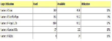
Table 3: Device utilization summary.
7. Conclusion and Future Scope
[image:6.612.325.544.370.451.2]© 2016, IRJET | Impact Factor value: 4.45 | ISO 9001:2008 Certified Journal | Page 625 ACKNOWLEDGEMENT
I take the opportunity to express my cordial gratitude to Ms. Sneha Nagar, Assistant Professor in the Department of Electronic and Communication Engineering, Oriental University, Indore (M.P.) for the valuable guidance and inspiration throughout the dissertation work. I feel thankful for his innovative ideas, which led to successful completion of this work.
I would also like to thank honorable Dr. Dhruva Ghai,
Dean Engineering
and Technology, Oriental University, Indore (M.P.) .References
[1] Design and simulation of UART serial communication module based on
VHDL - Fang Yi-Yuan, Chen Xue, IEEE Explore, may 2011. [2] Design and test of general purpose SPI master/slave IPs on OPB Bus- systems signals and devices, 7fu international multi conference, 2010. [3] A.K Oudjida et ai, Master-Slave wrapper communication protocol: A case-study, Proceedings of the 1'1 IEEE International Computer Systems and Information Technology Conference ICSIT'05, PP 461-467, 19-21 July 2006 .
[4] REN Yu-fei,ZHANGXiang,CHENGNai-ping (Department of Optical and Electrical,Academy of Equipment Command &Tech, Beijing 101416, China); Design and Realization of Two-way Transmission SPI Interface;
Telecommunication Engineering; 2009.
[5] Zhang Rui;A Method to Realize DSP Communicating with Other Device by SPI Interface
Protocol [J]; International Electronic Elements; 2003-08.
[6] A micro- FT-UART for safety critical SOC based Applications, www.doi.ieeecomputersociety.org.
[7] www.xilinx.comlsupport/documentationlip
documentationlxpspi.pdf