Kun-Yi Lee
1, Lung-Chien Chen
2*and Yu-June Wu
3Abstract
This investigation reports on the characteristics of MAPbI3perovskite films on obliquely sputtered ITO/glass substrates that are fabricated with various sputtering times and sputtering angles. The grain size of a MAPbI3perovskite film increases with the oblique sputtering angle of ITO thin films from 0° to 80°, indicating that the surface properties of the ITO affect the wettability of the PEDOT:PSS thin film and thereby dominates the number of perovskite nucleation sites. The optimal power conversion efficiency (Eff) is achieved 11.3% in a cell with an oblique ITO layer that was prepared using a sputtering angle of 30° for a sputtering time of 15 min.
Keywords:Oblique-angle sputtered ITO, MAPbI3perovskite, Wettability
Background
Indium tin oxide (ITO) is a transparent conductive ma-terial that comprises indium oxide (In2O3) and tin
oxide (SnO2). It is widely used in liquid crystal displays,
light-emitting diodes, and solar cells owing to its visible transparency of approximately 96% and conductivity of around 10 Ω/sq [1–5]. Several methods for improving the resistance and the transmittance of ITO films have been studied, including annealing and sputtering with various gas ratios and operating pressures [5–8]. The optoelectronic properties of obliquely sputtered ITO films have been reported upon [9, 10]. As an ITO film is deposited, it grows as a film with a tilted columnar structure at an angle on a substrate, owing to the shadow effect. The columnar ITO film exhibits a differ-ent morphology, anisotropic optical properties, and an-isotropic resistivity [10].
Recently, solar cells with perovskite materials, such as CH3NH3PbI3, as an active layer have received
much interest owing to their favorable power conver-sion efficiencies [11–18]. Most perovskite solar cells
have transparent conductive oxide (TCO) glass, such as ITO or FTO (fluorine-doped tin oxide), as the substrate. However, the optoelectronic properties of an isotropic TCO film differ from those of an aniso-tropic TCO film. Therefore, this work develops planar perovskite solar cells using CH3NH3PbI3 (MAPbI3)
perovskites on oblique ITO substrates that are pre-pared glancing angle deposition (GLAD). This investi-gation examines the optical, structural, and surface properties of MAPbI3 perovskite films on oblique
ITO substrates that have been annealed at various temperatures and sputtered for various times. The relationships between the performance of the perovsk-ite solar cell and the properties of the perovskperovsk-ite films are discussed.
Methods
In this investigation, ITO glass was cut into small pieces of size 1.5 × 1.5 cm2be used as substrates. The ITO glass substrates were thoroughly cleaned using acetone, ethanol, and deionized (DI) water in an ultra-sonic oscillator for 5 min and dried with nitrogen. An ITO film was deposited onto the ITO glass substrate by sputtering at various oblique angles using ITO tar-gets, as presented in Fig. 1a. The working gas and
* Correspondence:[email protected]
2Department of Electro-optical Engineering, National Taipei University of
Technology, 1, 3 Sec., Chung-Hsiao E. Rd, Taipei 106, Taiwan Full list of author information is available at the end of the article
pressure were pure argon and 5 mTorr, respectively. After deposition, the films were annealed at 300 °C for 30 min.
Glass substrates that were coated with the obliquely sputtered ITO films were used for the perovskite solar cells. PEDOT:PSS films were prepared by spin-coating the oblique ITO glass substrates at 5000 rpm for 30 s. After spin-coating, the film was annealed at 110 ° C for 10 min. The perovskite layer was deposited using two-step spin-coating onto the PEDOT:PSS/oblique ITO glass substrate at 1000 rpm for 10 s and 5000 rpm for 20 s. During the step at 5000 rpm for 20 s, the wet spinning film was quenched by dropping 100 μl of anhydrous toluene onto it. The perovskite precursor solutions were prepared
using 1.25 mmol methylammonium bromide and
1.25 mmol PbI2 (with a purity of 99.999%) that was
dis-solved in 1 mL cosolvent. The volume ratio of dimethyl sulfoxide (DMSO) toγ-butyrolactone (GBL) was 1:1. After spin-coating, the film was annealed at 100 °C for 10 min. Then [6,6]-phenyl-C61-butyric acid methyl ester (PCBM)
was dissolved in chlorobenzene (20 mg/mL) and spin-coated on perovskite layers at 3000 rpm for 30 s, forming a 50-nm-thick film as an electron transport layer. Finally, an
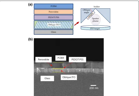
Ag electrode with a thickness of 20 nm was deposited by thermal evaporation to complete the structure of the device. The sample was covered with a shadow mask that defined an active area of 0.5 cm × 0.2 cm during the de-position. Figure 1a schematically depicts the complete
(a)
(b)
Fig. 1aSchematic cross section of completed structure and oblique sputtering system.bCross-sectional FESEM image of sample with 30°-tilted sputtered oblique ITO
Fig. 2XRD patterns of MAPbI3perovskite films on PEDOT:PSS/oblique
[image:2.595.58.539.86.419.2] [image:2.595.306.538.531.702.2]structure. Figure 1b shows the cross-sectional FESEM image of the sample with the 30°-tilted obliquely sputtered ITO.
Results and Discussion
The crystalline microstructures of the films were observed using an X-ray diffractometer. A field-emission scanning electron microscope (FESEM) was used to observe the surface morphology of the samples. The current density– voltage (J–V) characteristics of the solar cells were measured using a Keithley 2420 programmable source meter under irradiation by a 1000 W xenon lamp. The irradiation power density on the surface of the cell was calibrated to 1000 W/m2.
Figure 2 shows the XRD patterns of the MAPbI3
per-ovskite films on PEDOT:PSS/oblique ITO layer/glass at various oblique angles. The four mean peaks at 14.28°, 28.5°, 30.61°, and 31.93° correspond to the (110) per-ovskite, (220) perper-ovskite, (110) SnO2, and (222) In2O3
planes, respectively. As the sputtering angle increases from 0° to 60°, the (110) SnO2is formed by the
incorp-oration of Sn atoms. The size of the crystal domain can be calculated using Scherrer’s equation [19]. The sizes of the crystal domains of the MAPbI3 perovskite films in
the samples are approximately 71.8 nm. Therefore, the sizes of the crystal domains of the MAPbI3 perovskite
are not affected by the oblique ITO layer.
Figure 3 shows SEM images of MAPbI3perovskite films
on an oblique ITO layer/glass for various oblique angles.
(c)
(d)
Fig. 3a–dSEM images of MAPbI3perovskite films on PEDOT:PSS/oblique ITO layer/glass for various oblique angles
[image:3.595.58.538.88.350.2] [image:3.595.57.539.600.714.2]The grain (or particle) size of the MAPbI3perovskite films
increases with the oblique sputtering angle from 0° to 80°, revealing that the surface properties of the ITO influence the number of perovskite nucleation sites. Since the ITO is not in direct contact with the perovskite thin film and a PEDOT:PSS thin film is inserted between the ITO and the perovskite, the surface properties of the ITO should not directly influence the properties of the perovskite thin films. Hence, the wettability of the PEDOT:PSS thin films [20] is related to the surface properties of the ITO. Therefore, the different grain sizes in the MAPbI3 perovskite films may be related to the
wet-tability of the substrate [21, 22]. Experiments on the contact angle of a water droplet were carried out to assess the wettability of the PEDOT:PSS thin films
on the different ITO/glass samples, as shown in Fig. 4. The contact angle is proportional to the size of the grains in the MAPbI3 thin film, indicating
that the nucleation and crystal growth of a MAPbI3
thin film can be controlled by varying the surface wet-tability of the PEDOT:PSS/oblique ITO/glass. Contact angle images of the oblique ITO/glass samples were ob-tained to understand the variation of the surface wettabil-ity of the PEDOT:PSS/oblique ITO/glass samples, as depicted in Fig. 5. The wettability of the PEDOT:PSS/ob-lique ITO/glass samples is inversely proportional to the wettability of the oblique ITO/glass samples, so the vertical distributions of the hydrophilic PSS polymers and hydro-phobic PEDOT polymers can be manipulated by varying the surface wettability of the oblique ITO/glass sample. PSS polymers are suggested to be distributed mostly in the upper surface of the PEDOT:PSS thin film when the sub-strate has a hydrophobic surface (Fig. 5a), resulting in a small water droplet contact angle on the PEDOT:PSS thin film (Fig. 4a). The experimental results (XRD and SEM) demonstrate that the MAPbI3 grains are multi-crystalline
MAPbI3particles [23].
Figure 6 presents the photoluminescence (PL) spectra of the MAPbI3 perovskite films on PEDOT:PSS/oblique
ITO/glass for various oblique angles. One main peak is observed at 768 nm, corresponding to emission by MAPbI3. The finding is supported by the XRD results.
The PL emission energy of the MAPbI3perovskite is not
affected from beneath the oblique ITO layer. Addition-ally, the different PL intensities of the MAPbI3 films on ITOs sputtered with various oblique angles were ob-tained as a result of the separation of the light-induced exciton. A better interface between PEDOT:PSS and per-ovskite provided better exciton separation, inducing a Fig. 5a–dImages that show contact angle of water on oblique ITO layer/glass for various oblique angles
Fig. 6PL spectra of MAPbI3perovskite films on PEDOT:PSS/oblique
[image:4.595.59.540.87.283.2] [image:4.595.57.290.529.702.2]stronger PL quenching effect. Therefore, ITO at an ob-lique angle of 80° exhibited the best exciton separation from the perovskite layer to PEDOT:PSS, owing to the favorable surface wettability of the PEDOT:PSS/oblique ITO, as shown in Fig. 4.
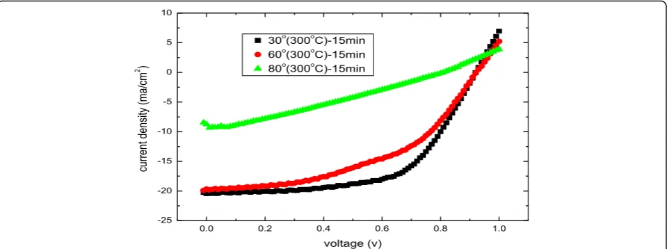
Figure 7 plots the current density–voltage (J–V) curve of the solar cells that are based on MAPbI3 perovskite
with an oblique ITO layer that is sputtered at various oblique angles and undergoes heat treatment at an an-nealing temperature of 300 °C. The sputtering time is 15 min. Table 1 presents the resulting power conver-sion efficiency (Eff ), short-circuit current density (Jsc),
open-circuit voltage (Voc), and fill factor (FF) of the
MAPbI3 solar cells. The performance of the device
degrades as the sputtering angle of the oblique ITO layer increases, because the oxygen content in the ob-lique ITO layers and their resistance increase with the sputtering angle [10]. Maximum efficiency can be achieved following deposition at an oblique angle of 30° owing to the favorable conductivity.
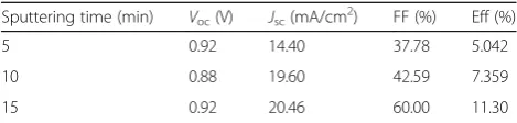
Figure 8 plots the current density–voltage (J–V) curves of the solar cells that are based on MAPbI3 perovskite
with the oblique ITO layer sputtered for various sputter-ing times, before undergosputter-ing heat treatment at an an-nealing temperature of 300 °C. Table 2 presents the corresponding power conversion efficiency (Eff ),
short-circuit current density (Jsc), open-circuit voltage (Voc),
and fill factor (FF) of the MAPbI3solar cells. Optimum
efficiency is reached when the sputtering time of the ob-lique ITO layer is 15 min because of the thickness of the layer and its good conductivity. The best device is ob-tained using this deposition angle, withJSC = 20.46 mA/
cm2,VOC= 0.92 V, FF = 60.00%, and Eff = 11.30%.
Conclusions
In summary, this work demonstrated the characteristics of MAPbI3 perovskite films on the
PEDOT:PSS/oblique-sputtered ITO/glass substrates that were fabricated using various sputtering times and sputtering angles. The device performance was optimized using an oblique ITO layer that was prepared by sputtering at 30° for 15 min, with a short-circuit current density (JSC) = 20.46 mA/cm2,
[image:5.595.306.538.534.704.2]open-Fig. 7Current density–voltage (J–V) of solar cells based on MAPbI3perovskite with oblique ITO layer sputtered at various oblique angles
Table 1Parameters of perovskite MAPbI3film on oblique ITO layer with various oblique angles
Oblique angle (°) Voc(V) Jsc(mA/cm2) FF (%) Eff (%)
30 0.92 20.46 60.00 11.30
60 0.922 19.68 49.11 8.91
80 0.80 8.75 31.06 2.19
Fig. 8Current density–voltage (J–V) of solar cells based on MAPbI3
[image:5.595.56.291.676.732.2]circuit voltage (VOC) = 0.92 V, fill factor (FF) = 66.0%, and
power conversion efficiency (Eff) = 11.3%. The perform-ance of the device degrades as the sputtering angle of the oblique ITO layer increases from 30° to 80° because the resistance of the device increases with the sputtering angle. Although oblique ITO layers improve the scattering of incident light, the high resistivity degrades the perform-ance of the device. Therefore, optimum efficiency can be achieved by deposition at an oblique angle of 30° owing to the conductivity.
Abbreviations
FESEM:Field-emission scanning electron microscope; GLAD: Glancing angle deposition; ITO: Indium tin oxide;J–V: Current density–voltage;
MAPbI3: CH3NH3PbI3; PEDOT:PSS: Poly(3,4-ethylenedioxythiophene)
polystyrene sulfonate; TCO: Transparent conductive oxide; XRD: X-ray diffractometer
Acknowledgements
The authors gratefully acknowledge the financial support from the Ministry of Science and Technology of the Republic of China under Contract No. NSC 106-2221-E-027-091.
Funding
This work was supported by the financial plan of the Ministry of Science and Technology of the Republic of China.
Authors’Contributions
KYL and LCC prepared the figures. LCC wrote the paper, designed the experiments, and analyzed the data. YJW prepared the samples and did all the measurements. LCC and KYL made the discussion and suggested the parameter. All authors read and approved the final manuscript.
Ethics Approval and Consent to Participate
Not applicable.
Competing Interests
The authors declare that they have no competing interests.
Publisher’s Note
Springer Nature remains neutral with regard to jurisdictional claims in published maps and institutional affiliations.
Author details
1Department of Electrical Engineering, China University of Science and
Technology, No. 245, Sec. 3, Academia Road, Taipei 115, Taiwan.
2Department of Electro-optical Engineering, National Taipei University of
Technology, 1, 3 Sec., Chung-Hsiao E. Rd, Taipei 106, Taiwan.3Graduate
Institute of Optomechatronics Engineering, China University of Science and Technology, No. 245, Sec. 3, Academia Road, Taipei 115, Taiwan.
Received: 31 August 2017 Accepted: 24 September 2017
References
1. Cui HN, Teixeira V, Meng LJ, Martins R, Fortunato E (2008) Influence of oxygen/argon pressure ratio on the morphology, optical and electrical
properties of ITO thin films deposited at room temperature. Vacuum 82: 1507–1511
2. Lewis BG, Paine DC (2000) Applications and processing of transparent conducting oxides. MRS Bull 25:22–27
3. Limmer SJ, Cruz SV, Cao GZ (2004) Films and nanorods of transparent conducting oxide ITO by a citric acid sol route. Appl Phys A Mater Sci Process 79:421–424
4. Cui HN, Xi SQ (1996) The fabrication of dipped CdS and sputtered ITO thin films for photovoltaic solar cells. Thin Solid Films 288:325–329
5. Gorjanc TC, Leong D, Py C, Roth D (2002) Room temperature deposition of ITO using r.f. magnetron sputtering. Thin Solid Films 413:181–185 6. Kim SM, Rim YS, Keum MJ, Kim KH (2009) Study on the electrical and
optical properties of ITO and AZO thin film by oxygen gas flow rate. J Electroceram 23:341–345
7. Minami T, Sonohara H, Kakumu T, Takata S (1995) Physics of very thin ITO conducting films with high transparency prepared by DC magnetron sputtering. Thin Solid Films 270:37–42
8. Danson N, Safi I, Hall GW, Howson RP (1998) Techniques for the sputtering of optimum indium-tin oxide films on to room-temperature substrates. Surf Coat Technol 99:147–160
9. Barranco A, Borras A, Gonzalez-Elipe AR, Palmero A (2016) Perspectives on oblique angle deposition of thin films: from fundamentals to devices. Prog Mater Sci 76:59–153
10. Chen LC, Chen CC, Sung YT, Hsu YY (2009) Oblique-angle sputtering effects on characteristics of nanocolumnar structure anisotropic indium tin oxide films. J Electrochem Soc 156:H471
11. Hodes G (2013) Perovskite-based solar cells. Science 342:317–318 12. Chen LC, Tseng ZL, Chen CC, Chang SH, Ho CH (2016) Fabrication and
characteristics of CH3NH3PbI3perovskite solar cells with
molybdenum-selenide hole-transport layer. Appl Phys Express 9:122301
13. Yang WS, Noh JH, Jeon NJ, Kim YC, Ryu S, Seo J, Seok SI (2015) High-performance photovoltaic perovskite layers fabricated through intramolecular exchange. Science 348:1234–1237
14. Liu M, Johnston MB, Snaith HJ (2013) Efficient planar heterojunction perovskite solar cells by vapour deposition. Nature 501:395–398 15. Im JH, Jang IH, Pellet N, Grätzel M, Park NG (2014) Growth of CH3NH3PbI3
cuboids with controlled size for high-efficiency perovskite solar cells. Nat Nano 9:927–932
16. Jeon NJ, Noh JH, Yang WS, Kim YC, Ryu S, Seo J, Seok S II (2015) Compositional engineering of perovskite materials for high-performance solar cells. Nature 517:476–480
17. Chen LC, Tseng ZL, Huang JK (2016) A study of inverted-type perovskite solar cells with various composition ratios of (FAPbI3)1−x(MAPbBr3)x. Nano 6:183
18. Tong X, Lin F, Wu J, Wang ZM (2016) High performance perovskite solar cells. Adv Sci 3:5
19. Zhang Z, Wang CC, Zakaria R, Ying JY (1998) Role of particle size in nanocrystalline TiO2-based photocatalysts. J Phys Chem B 102:10871–10878
20. Chang SH, Chen W-N, Chen C-C, Yeh S-C, Cheng H-M, Tseng Z-L, Chen L-C, Chiu KY, Wu W-T, Chen C-T, Chen S-H, Wu C-G (2017) Manipulating the molecular structure of PEDOT chains through controlling the viscosity of PEDOT:PSS solutions to improve the photovoltaic performance of CH3NH3PbI3solar cells. Sol Energy Mater Sol Cells 161:7–13
21. Bi C, Wang Q, Shao Y, Yuan Y, Xiao Z, Huang J (2015) Non-wetting surface-driven high-aspect-ratio crystalline grain growth for efficient hybrid perovskite solar cells. Nat Commun 6:7747
22. Lee K-M, Chen C-C, Chen L-C, Chang SH, Chen K-S, Yeh S-C, Chen C-T, Wu C-G (2017) Thickness effects of thermally evaporated C60thin films on regular-type
CH3NH3PbI3based solar cells. Sol Energy Mater Sol Cells 164:13–18
23. Chen CC, Chang SH, Chen LC, Cheng HM, Tseng ZL, Wu CG (2016) Manipulating multicrystalline grain size in CH3NH3PbI3thin films for
[image:6.595.56.291.109.165.2]application in photovoltaics. Sol Energy 139:518–523
Table 2Parameters of perovskite MAPbI3film on oblique ITO with various sputtering times
Sputtering time (min) Voc(V) Jsc(mA/cm2) FF (%) Eff (%)
5 0.92 14.40 37.78 5.042
10 0.88 19.60 42.59 7.359