-GENERAL PRECISION
I
LIBRASCOPE GROUP808 WESTERN AVENUE, d:t-ENPALE 1, CALIFORNIA
Technical Description
Technical Description
L-1192 CONTROLLER PROCESSOR
SURFACE EQUIPMENT DIVISION
<@>
@~~@~&~
[JDlRl~©D@O@~ T~~
Sec tion 1.0 2.0 3.0 4.0 CONTENTS
INTRODUCTION . . . .
SUMMARY OF APPROACH
2.1 Word Format . . . .
2.2 Instruction Efficiency
2.3 Comrnunication Interface
2.4 2.5 2.6 2.7 2.8 2.9
Code/Forrnat Flexibility
I/O Stations
Con1lT1unication Proc e s sing
I/O Interface . . . .
Support Software.
AUTODIN Processing
EOUIPMENT DESCRIPTION AND OPERATI00J
3. 1
3.2
Co re Menlo ry
L-1192 Controller -Processor
3. 2. 1 3.2.2 3.2.3
3.2.4 3.2.5
3.2.6
Arithmetic and Logical Unit Con1m unic a tion Inte r fac e. Pape r Tape, Typewrite r, and Card/Print
r/o . . . .
I/O Interface . . . . L-1192 ivlaintenance Panel L-1192 Interval Tin1er
L-1192 II\STRUCTI00JS . . . .
4.1 Fixed Length Character Operations
4.2 Variable Field Operations
4. 3 Full Word Ope rations
4.4 Program Control Operations
4. 5 Inte rnal Condition Ope rations
4.6 Con1munication Interface Operations
4.7 Input/Output Operations
Page
1 - 1
Section
5.0
CONT ENTS - Continued
PERIPHERAL EQUIP~1SNT
5. 1
5.2
5.3
Line Unit Console
Model 2250 Systen1atics Card/Printer Input/ Output Stations . . . .
5.2.1 Operating iYlocles 5.2.2 Operating Speed 5.2.3 Station Devices
Magnetic Tape Console
5. 3. 1 5.3.2 5.3. 3
Tape Transport On-Line Read Tape Transport On-Line \Vrite Tape Transport Off-Line Operation (optional) . . . . . .
5.4 Card Reader/Punch Console
5.4. 1 5.4.2
Card Reader Card Punch
5.5 High-Speed Printer Console
5.6 Master Disc File Console . . .
6.0 SUPPOR T SOFTW ARE AND PROGRfuV11,110:G DESCRIPTION
7.0
6. 1 LAP-1192 Assembler 6. 1. 1
6. 1.2 6. 1. .3
6. 1.4
6. 1. 5
6. 1.6
6. 1. 7
Purpose . . . . Equipn1cnt Required Input l'v1edia . .
Output iYledia Features . . . Input Forn1at P scudo -Ope ration
6.2 Systen'l Loader . . . .
6.3 Co re and Di sc Dump
6.4 Acceptance Tests
AUTODI.:-\ PROCESSIl\"G
7. 1 Input Processing
7.1.1 Character Frame . . 7. 1. 2 SY,stem State s . . . .
Page 5-1 5-1 5-2 5-2 5-3 5-3 5-5 5-6 5-8 5-8 5-9 5-9 5 -1 1
5-11
5-13
6 -1
6 -1
0-1
6 -1 6 -1
6 - 1
6-2 6-3
6 -3
Section Figure 3 -1 3 -2 3 -3 3-4 4-1 5 -1 5-2 5-3 5-4 7-1 7-2 7-3 7-4 7.2 7.3
CONTENTS - Continued
7.1.3 Start of Block Processing . . 7. 1.4 Data Cha racte rs . . . 7.1.5 End of Block Operations
Output Processing . . . .
7.2.1 Character Frame . . . . . 7.2.2 Start of Block Processing . . 7.2.3 Data Characters . . . 7.2.4 End of Block Operations . .
Channel Coordination . . . .
7.3. 1 Input Channel Coordina tion 7.3.2 Processing of RM and DM
7.3.3 Establishnlent of Acknowledge Sync on Startup. . . . . .
ILLUSTRA TIONS
L-l192 Buffer Processor Console - Front View.
L-l192 Buffer Processor Console - Rear View
L-ll92 Buffer Processor, Block Diagranl.
L-1192 Maintenance Panel
Register Selection . . .
Magnetic Tape Console Control Panel
Card Reade r jPunc h Console. High-Speed Printer Console.
File Disc Showing Installation of Hear Bar Asserrlblies . . . .
AUTODI:0J Program ... Overall Flowchart.
Input Character Processing.
Output Character Processing
Channel Coordination Processing
Page 7-4 7-5 7-5 7-6 7-6 7-6 7-8 7-8 7-8 7-10 7 -11
7-14
Page
3-2
3 -3
3-5
3 -1 1
Section 1
INTRODUCTION
This document pre sents a technical de scription of the L-1192 Controlle
r-Proce ssor system. The Librascope de sign approach is based primarily
on experience gained frorn their L-3055 data processing system. This
equipment was developed and installed in the Pentagon as the AN/FYQ-ll
data processing elements of Command and Control System 473-L.
Exten-sive effort was expended to structure and create a system which will
function reliably and continuously without 10 s s of se rvice .
The L-1192 system provide s a stored-program binary compute r, with both
an AUTODIN communication interface and general purpose processing
capa-bility. It will ope rate as a communication buffe r to the L-3155 Central Processor in the 473-L system, and can also provide this function for
other available processing systems. The L-1192 Controller-Processor
may also be utilized as a general-purpose computer on its own. It will
inte rface with a variety of communication channels, input-output stations,
and peripheral devices. These include asynchronous and synchronous
lines, paper tape/card/typewirter
r/o
stations, magnetic tape transports,card reader/punches, disc files, and high speed line printers.
A description of the L-3l55 Central Processor, which provides eight 7-bit
alphanumeric characters per computer word, is provided under separate
cover.
Section 2
SUMMARY OF APPROACH
The L-1192 Controller Processor is a general purpose computer system,
'with special emphasis on the efficient processing of input-output and
communica tion cia ta.
2. 1 . WORD FORlv1A T
The L-1192 provides 2 microsecond cycle cone memory In n10dules of
4096 \vords, with a maximum capacity of 65,536 words. The 33 -bits per
word includes 32 data bits, providing four 8-bit characters, plus one
parity bit. This word length perrnits an instruction format well suited
to character processing and addressing.
2.2 INSTRUCTION EFFICIENCY
The L-1192 offers three categories of processor instructions: single
char-acted operations, variable-length field operations, and full-word operation.::>.
The single character instructions utilize a group of eight arithmetic
regis-ters, which eliminates the bottleneck normally encountered in processing
rnultiple input-output data.
2.3 COMMUNICATION INTERFACE
The L-1192 Console can conlmunicate with up to four duplex
comnlunica-tion channels, by the addicomnlunica-tion of the proper interface modules. This
capa-t)ility can be expanded to 64 duplex channels by rneans of an optional Line
Unit Console. Any rnix of asynchronous and synchronous line s is
per-missible. Asynchronous lines operate up to 150 bits/sec, and synchronous
line s at up to 4800 bits/sec.
2.4 CODE/FORMAT FLEXIBILITY
The L-1192 has been designed to efficiently process AUTODII\
conHnunica-tion requirements. Care has been exercised to perrnit flexibility of
operation through program modification. Desired character codes,
for-mats, and channel coordination procedures are under control of the stored
program.
2.5 I/O STATIONS
The Standard Communication Inte rface will also communicate with up to
eight input/output stations, which may be located at remote positions.
One station is utilized by the 300 char/sec paper tape reader, 60 char/sec
paper tape punch, and 15 char/sec electric typewriter at the Operator/
Maintenance Panel. The othe r seven stations may each provide a 20 char /
sec card read/punch and a 40 char/sec print station, or other desired
I/O characte r device.
The number of I/O stations may be expanded in groups of 8 to a total of 32.
2.6 COMMUNICATION PROCESSING
Input characters and output reque sts for the communication channels and
the I/O Stations automatically enter cyclic. Channel Activity Tables
re-serve-d in core memory. These entries do not interrupt the system, and
are accessible to the computer program for further processing.
2.7
r/o
INTERFACEOne I/O Interface is provided with the L-1192 Controller Processor, and
up to sixteen interfaces may be utilized. Each interface may communicate
with up to sixteen standard Librascope peripheral devices. These include
magnetic tape, card reader/punch, high- speed line printer, and disc file
equipment.
2.8 SUPPOR T SOFTWARE
The support so~tware offered with the L- 1192 system includes an Assembler,
a System Loader, Core and Disc Dump, and Acceptance Test.
2.9 AUTODIN PROCESSING
Librascope has had extensive experience in processing communication
data, and will be available to assist in Dleeting AUTODLN requirements.
An operational approach developed for the L-1192 sy stem is pre sented
in this proposal.
Section 3
EQUIPMENT DESCHIPTION A0;D OPERATIO;..J
This section discusses the design and operation of each itern of equiprnent
available with the L-1192 Controller-Processor system.
3.1 CORE MEMORY
Core rnelnory for the. L-1192 Controller-Processor systern is provided in
rnodules of 4096 words. The L-1192 rnay <lddress up to a maxirnuD1 of
six-teen rnodules, for a total of 65,536 words of mernory. A word contains 32
data bits plus an additional bit to maint<lin odd parity. Each data word
pro-vides four 8-bit characters, which rnay be individually addressed by L-1192 instructions. Transfers to and frorn core rnenl0ry are in word parallel,
and these are parity checked. The core memory nlodules offer a
read-write cycle time of 2. 0 microseconds. The transfers between core
rnem-ory and the central processor arithn1etic/logical unit, the comn1unication
interface, and the input-output interface all overlap on a cycle stealing
basis.
3.2 L-1192 C00JTROLLER-PROCESSOR
The L-1192 Controller-Processor consists of an Arithmetic and Logical
Unit, a Communication Interf~ce, Paper Tape Reader/Punch and Electric Typewriter, an I/O Interface, and the Maintenance Panel, and
an
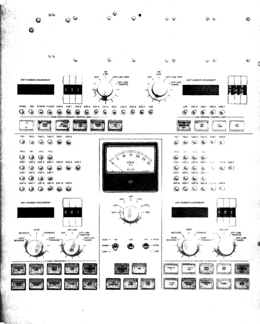
IntervalTimer. The L-1192 Console is presented in Figures 3-1 and 3-2.
3.2. 1 Arithmetic and Logical Unit
The L-1192 ALU includes the instruction register and instruction decode
logic, individually addressable character-length data registers, a Field
Operand Address Register, and two full-word arithmetic registers.
The simple yet flexible organization of the L-1192 is apparent fronl the
block diagram of the processor organization, presented in Figure 3-3 any
operations which involve two operands can'be obtained in any conlbination
from the data or word registers and Dlclnory by general bus logic. The
INPUT-c: .. npUT \"::L [1 t ,':;-s
Mm IlH'Ul r'(,;,:.~n r.::~ f,
[image:11.807.71.733.52.545.2]W
I
V.I
cr~RD P.ACI\
function of address modification is also performed by this technique.
Com-lTIunication with the core melnory is by an address and word bus which is
tinl.e shared with the ComlTIunications Interface and with the
r/o
Interface.3.2. 1. 1 Data Format. Each L-1192 word consists of 32 data bits plus
one parity bit. Four 8-bit data characters are contained in a word, and
these characters rnay be individually selected by the L-l192 instruction.
8 8 8 8
Character Character Character
I
Character4 3 2
I
1P
3.2. 1.2 Instruction FonTIat. Instructions are one word in length, and
pernl.it register selection in addition to melTIOry word addressing. Special
features of the instruction set include direct character selection, word
and character indexing, indirect addressing for both memory and registers,
and the inclusion of specialized instructions.
3.2.1.3 1v1emory Addressing. The address field of an instruction provides
for direct reference to anyone of 65,536 words of core memory. In
addi-tion, 2 bits appended to the low order end of the addre s s field pe rrr.it the
selection of an individual character within the word. This feature provides
full-character addressing.
3.2.1.4 Processor Instructions. The L-1192 offers three categories of
processor instructions. Fixed length character instructions primarily
provide single-character transfer, arithn'letic, and logical operations.
These facilitate the processing of data from rnultiple comnl.unication lines
and direct-coupled paper tape, punched card, and typewriter/printer
de-vices. A set of variable field (up to 16 character) instructions provide
added formatting and editing capability for both comnl.unication and
input-output, devices. Word-length operations are, also provided to nl.eet higher
speed processing requirements.
I
CORE ME~;ORY'
LO~6WO~
.... ~.
~
,'J WORD BUS C4 C3 C2 C:
~~-~~~~~~~~~~~--~~~~~~~~-~~~. :~:~:.,.~l TO I/O
~ \ t i n ' " '"''''I
i . ' ,. I ~,'''' OJ.., ....
_ _ _ _ _ _ _ _ _ _ _ _ _ _ _ A_D_J_R_E_S_S_8_U_S_; '"
'-J
lNTERF't..CES I! .. "~ i
ij :'
.:
.
~
. ~
---
---
...---
---I
---1:-::.
CO~JTROL
'"'---,->
FiELD OPERAND t.DGRESS REGISTER
VAR1A8~E FiELD
OPER~TIOi\S O?Tl0N LOGiCt..L A~;D ARITH~,:ETIC O?ERATICNS
\ 1
1
i V:ORD REG.
~
11
Ij
~:!
LR_--.J
RESULT SUS
V,'O:::\') ;:::G. ,
Q
I
' - - - -- - - '
I
!
i
I
I. \
i"·-1-I
I_ _ _ _ _ _ _ _ _ 1
i
I
I
I
Figure 3-3. L-1192 Buffer Processor, Block
Diagrarn
[image:14.617.87.556.44.703.2]3.2.1.5 Specialized Instructions. Several of the L-1192 instructions have
been specialized in order to enhance speed-cost effectiveness in
CODlnluni-cation and input-output processing. The inc;us;on of these instructions
con1bine the advantages of wired logic with tilt' flexibility of stored program
control. An Initiate Character Cycle instructic::'l1, for example, will
effi-ciently locate and access the next input character or output request to be
pro c e sse d . The sewer e auto 11l. a tic all y s tor e din cor e me In 0 rye han n c 1
Activity Tables (CAT) by the L-1192 hardware.
3.2.1.6 Character D;')ta Registers. The L-1192 IS provided with a set
of 8 character-length static registers, which are basic to its list of
power-ful character processing instructions and capabilities. Any of the 8
reg-isters rnay be utilized in arithrnetic, data, or logical operations. Most
operations involve a single register and a location in core rnemory.
Op-erations rnay also be specified which involve only a pair of registers, or
a register and an operand or Inask contained in the instruction word itself.
These features serve to reduce the alnount of time normally consurned by
cornputers in the access and storing of operands in core rnemory. The
unusually high character processing efficiency of the L-1192 is attained by
making up to 8 separate data items inl.mediately available to the arithnletic
unit.
The d a t a r e g i s t e r sma y a 1 so fun c t ion as in de x reg i s t e r s . \\1 hen use d a s index registers, four of the 8-bit data registers operate independently.
Eacn can provide a total nlodific ation of 256 charac te r or 64 -wo rd
ad-dresses. The remaining four are paired to provide two la-bit index
reg-isters, each with an addressing capacity of 65,536 characters. Indirect
addressing is also a feature of the L-lI92, and rnay extend over any
nlim-ber of levels. Indexing is effective at each indirect level.
3.2.1.7 Addition;tl Registers. The variable field instructions provide
lnen10ry to rnemory operations. One operand rlddress and field length is
nOTI'nally specified by the instruction word. Tl .... e second operand address
and field lengthmustfirst be loaded into a Field Operand Address
Regis-ter (FOAR). The fulf-word instructions utilize two independent word
arithrnctic registers (R and Q). The variable field instructions and the full-word instructions also utilize the character data registers as index
re gis ter s. They are available as a r ithrne tic re gi s t(~ r s only to the fixe d length character instructions.
3.2.1.8 Error Checks. To insure rnessage protection, the L-1192
em-ploys several internal error checks. These include an automatic test of
wo rd pa ri ty whe n a word is t ransfe rred frorn core rnelTIOry, and pa. r ity
checks on transfer operations between the L-l192 and the I/O peripher;d
devices. PrograrTI testing is norrnally utilized to parity check
charac-ters received frorn the cornmunication lines.
3.2. 1.9 Interrupts. To permit efficient servicing of the Input-Out1)ut and
Cornn1unication Interfacps, a nun1ber of interrupts have been provided.
The con d i ti 0 n s w h i c h c an c au sean in t e r ru p t inc Iud e : In te r val T i n1 e r elapsed, I/O operation ended, service requests from the peripheral
de-vices, and internal or input-output parity error.
When an interrupt occurs, the content of the P counter and a bit
indicat-ing the cause of the interrupt are stored in core memory location
¢,
andthe next instruction is taken from location 1. All other interrupts are then
prevented fro1'n occurring. They may be enabled by use of the ESI or PSI
instructions.
3.2.2 Con1n1unication Interface
The Co1'nmunication Interface is contained in the L-1192
Controller-Processor Console. It controls the transfers of data between core H1en10ry
and on-line cornmunication channels or devices.
The basic sys tern can accornmodate four input and four output con1nl unic
a-tion. channels, by the addition of optional Line Interface :V10dules. ;-':odules
may be specified for asynchronous or for synchronous tra.nsmission at
rates up to 4800 baud. The cornnl.unication interface caIJability can be expanded by the addition of an optional Line Unit Console, \vhich can
ac-commodate up to 64 input and 64 output cornnl.unication interface 1110dules
and channels.
3.2.2.1 C0re Buffering. Character buffering is provided by the interface
Inodules, while rnessage blocks are acculnulated in core H1ernory. This
approach results in significant saving in systenl cost, and perrnits the
prograrn. to operate asynchronously with line rates.
The core buffering operation is perforrTlcd in a unique and efficient
rnan-nero Two cyclic table areas, narned Channel Activity Tables, are
re-s e r v e din cor e n1 e 1110 r y . The sea rea u to mat i c a 11 y 10 ad e d by the Corn rn u n i -cation Interface with the input characters or with requests for output
characters, each with a line identity nun1ber. Channel Activity Table
(CAT 1) is reserved for character requests rnade by high speed output lines. Channel Activity Table 2 (CAT 2) is used to buffer all other lower
priority output requests and all input traffic. CAT 1 rnay contain 128 entries or words in melnory, while CAT 2 has a capacity of 256 entries.
3.2.2.2 Cornrnunication Line Servicing. The Con1nlunication Interface
rnakes use of two cyclic load address registers designated Ll and L2, for
CAT 1 and CAT 2 control respectively. Each time an entry is to be stored
in either table, the appropriate load counter provides the required core
loading addre s s and is then stepped. CAT 1 and CAT 2 are unloaded and
proc e s s ed by 1neans of two other c yc lic addre s s counter s, na~ned Uland U2 .. A 1110re detailed discussion of the procedure for unloading of CAT 1 and CAT 2 is contained in the discussion of the Initiate Character Cycle
instruction, found in Section 4.6.
The output characters transmitted 111 response to output requests rire
auto-rnatically obtained from another table, named the Line Character Buffer
Tab 1 e . Th e LC B T con ta ins 0 ne ass j g ned c h a r act era d d res sin cor e 1"n e n1
-ory for each output line implernented. These output locations are 10Clded
by the program with the next output character for the corresponding line
nu1'nber. When an output interface module has completely transrnitted an
output character it initiates an interface available signal, w11ich will be
detected by and halt the scanners in both the Line Unit Console and in
Corn-rnunication Interface. The two scanner positions will generate th.e proper
character memory address in the LCBT, and the character at tt'}.ls position
will transfer to the waiting output line interface module. The
Communi-cation Interface will then load an output request, including the line
identi-fication number, into CAT 2 (for high speed lines) or into CAT 1 (for slow
speed lines). The Ll or L2 load point is stepped, and the scanners are
released to continue searching for .other input or output traffic. Input
traffic is handled in a somewhat similar manner by the Communication
Interface. When a complete character has been accumulated by an input
line interface module, it sets a signal causing the scanners to stop.
Mem-ory access is obtained, and the character plus the associated line number
is automatically transferred to the next available word location in CAT 2.
The L2 load point is stepped, and the scanners are then released to
con-tinue looking for traffic. The input character will be processed by the
L-1192 program, whose instructions can efficiently access the next input
character or output request ~rom the two Channel Activity Tables.
3.2. 2. 3 Channel Activity Table Formats. The following information
pro-vides the word formats loaded into the Channel Activity Tables (CAT) for
the input characters and the output requests.
Input Entry
Output Request
3.2.3
8 8 8
I
I
Line/Devic e
Not Used I 0 Input Char.
I Address
1
I
I Line/Device
Not Used I 1 Always Zero
I Address
I
Paper Tape, Typewriter, and Card/Print I/O
The basic Communication Interface also communicates with up to eight
direct-connected input-output stations, which may be located at remote
sites. The number of such stations accessible to the communication
inter-face may be optionally increased in groups of eight up to a total capacity
of 32 such stations. The paper tape reader, punch, and IBM keyboard/
typewriter at the computer console provide one station position. A
Kleinschmidt keyboard/printer, and a card reader/punch may be located
at each of the othe r seven station po sitions. The se stations will, howeve r,
accept other input-output devices which contain the prope r
interface.. Transfers to or from these devices are character-serial, with
up to 8 bits/char.
3.2.4 I/O Interface
The I/O Interface provides for data transfers to and from the standard line
of Librascope magnetic tape, card reader/punch, line printer, and disc
file equipment. These peripheral devices are presently utilized in the
Librascope AN/FYQ-ll Data Processor.Set for the Headquarters U. S.
Air Force 437 -L Command and Control System. All,data transfer to and
froITl these devices occur on an asynchronous basis, with the I/O interface
obtaining memory access priority as needed . . The I/O interface will
in-dependently execute interface block transfers, and overlap central
proc-essor operations.
3.2.4.1 Description. The I/O interface contains a Device COITlmand
Register, a Block Control Register, an Interface Data Register, a
Com-mand Address Register, and associated control and bus logic. Once the
interface has been placed in operation, it will access a device COITunand
Word and a Block Control Word from core memory. The Command Word
specifies the device and command operation. The Block Control word
designates the memory starting address and the required number of
characters. Data is shifted into or out of the Interface Data Register In
a character-serial fashion on a device demand basis. As data is
trans-ferred, the Block Control Register counts characters and memory
loca-tions. When the Block Control word is, satisfied, the operation is
ter-minated and the rnain processor program is interrupted.
3.2. 5 L-1192 Maintenance Panel
The maintenance panel, presented in Figure 3 -4, contains the necessary
controls and indicators for performing preventive or corrective
mainte-nance on the L-1192 Controller-Processor and its interfaces. By means
of the se controls and indic ator s, the various internal register s are
dis-played and their contents may be altered. In addition, L-l192 error
WORD REGISTERS
P C4 C3 C~ CI
PROGi\~ :,~
COUNTER
( ) ( ) 6
( ) 7
o
~)C)OC)3
OQJ(ju
20000,
DISPLAY CU::"R STC,,';: CLEAR
o
HiCK -10
NOR>A l,f) ~
~
LOW
!n
V
o
0
((
'\\
il~li
i
l ..
J
!
!
Il
J
-;:.':; +10
(0)
t::::I
@
INST R:'::G
CL:AR EXECUTE
o
0
WORD REGISTER
Ri::G: S-jERS ?-'",:,
«,,J b
C;;
7Cd
G("". ~
':-".,;1 ;;J
0"
0
30
20
1 CLE.\Ro
cE~C:~'
F~I\LI G UiH : L2.
DATA REGISTER
IN'':'cRr:'CEO:
ERAOR '>-j
1 LC:'D:
I
P;,:,;"I
[image:20.618.96.537.77.568.2]~
indicators rnay be reset fron1 thi::> panel. The output voltages of the
vari-ous power supplies rnay be 11leasured, and their outputs biased to assist
in detecting n1achine lTIalfunctions. Tbe following paragraphs descrihe in
detail the functions of the various controls and indicators on the
rnttinte-nance panel.
3.2.5. 1 "'lord Register Display and Switches. An array of 33 pushbutton
indicator/switches displays the content of the specified word register.
Selection of the Memory Access Register (M), the Field Operand Access
Registers (F), or the word artluTIetic Rand Q Registers is by means of
a "\Vord Register!' select switch. The display is arranged into 4
char-acters of eight bits each and the parity bit. An associated error indicator
i s i 11 U 111 ina ted w hen the rll ern 0 r y reg i s t e r i s s e 1 e c ted and con t a ins a par i t Y fault c ondi tio n (even nunl be r of bi ts ). Di rec t lTlanual rnemory entry is
performed using the Clear and Load pushbutton switches. The Clear
pushbutton clears the selected register to binary zeros, except for the
parity bit which is a binary one to n1aintain required odd parity. Tbe
desired word is then set by pushing appropriate register pushbuttons.
Pushipg the parity pushbutton will set the correct parity bit and reset the
error indicator.
Pressing the STORE pusbbutton stores the contents of the selected
regis-ter into the address specified by the W portion of the Instruction Regisregis-ter.
W is then incrernented by one. The content of the rnemory location
speci-fied by \V n1ay be di splayed by pre s sing the DISPLAY button, which also
causes W to incrernent by one.
3.2.5.2 Progranl Counter Display and Controls. An array of pushbutt.on
indicators displays the content of the prograln counter. The "PROGRAlvl
COU0JTER" display can be set to zero by the associated "CLEAR"
push-button and new content set in n1anually.
3.2.5.3 Instruction Register Display and Controls. An array of
push-button indicators displays by fields the content of the instruction register.
The "INST REG" display can be cleared by the associated !rCLEAR!'
pushbutton and new content set in Inanually. The currently contained
in-struction can be executed in stop H10de by pushing the "EXECUTE" button,
pern1itting instruction processing without counting up the progranl counter
or leaving the stop n1ode.
3.2.5.4 Operand Registers Display and Controls. The "OPERAND
REGISTERS" display pushbutton indicators Inay be used to observe the
content of any of the 8 Data Registers, or the content of the two Load and
Unload Counters associated with the con1n1unication interface. Selection
of register or counter to be displayed is controlled by a rotary" DA T A
REGISTER" switch below the "OPEHAND REGISTERS" indicators. The
re gi s te r cur rentl y di splayed n1ay l1a ve its content c learecl to ze ro by means
of the "CLEAR" pushbutton and a new content manually entered.
3.2.5.5 Error Indicators. The three error indicators in the lower
right-hand section of the panel display detail errors detected by the L-1192
hard-ware. The "INTER~AL PARITY ERROR" indicator will light whenever the L-1192 hardware detects a word parity error on transfers to or frorn
core memory.
The "II':TERFACE ERROR" indicator will light whenever the L-1192
inter-face logic detects a character parity error on input':'output data transfers.
The "TnvlER ERROR" indicator will light whenever the INTERVAL TIMER
counts down to zero.
3.2.5.6 Operating Controls. The ON and OFF buttons control the
appli-cation of power. Pressing the RUN button will cause the L-1192 to locate
ar.d execute instructions at norrnal operating speed until either a HALT
cornmand is decoded, the STOP button is pn':":::i(;d, or ::1n internal error is
detected. The STEP button will cause a singL .. ~ instruction to be executed each time the button is pressed. Operation of the ERROR CLEAR will
reset all error toggles.
3.2.5.7 l;::rror Controls. The "ERROH CLEAR" pushbutton resets all
error indicators.
The "IGNORE ERROR" pushbutton disables the halt on instruction parity
error and rnay be used while operating diagnostic or rnaintenance progran1s.
3.2. 5.8 Power Supply I",ionitor and Controls. By rneans of the a::;sociated
selector switch, output voltages of the v<lrious power supplies in the L-1192
Hlay be displayed on the n1eter on the lower left-hand portion of the
rnain-tenance panel. Toggle switches are provided to control increase or
de-crease of power supply voltages in the diagnosis of machine malfunctions.
3.2.6 L-1192 Interval Timer
The L-1192 Interval Tilner is an electronic counter operated by the n-:..aster
logic clock. It is composed of 32 bits (one word). It counts down by one during each clock period. It can be pre-set under prograrr. control via the
I/O interface, and its current value can similarly be stored in core.
The Inaximum. pre-set value is equivalent to approxiHlately one hour.
Re-solution is approxinlately ten tiHles greater than the instruction execution
rate.
Section 4
L-1192 INSTRUCTIONS
The de taile d de sc r i ption s of L -1192 in structions have be en groupe d unde r the following gene ral categorie s:
1. Fixed Length Character Operations
2. Variable Field Operations
3. Full Word Ope rations
,
4. Program Control Operations
5. Inte rnal Condition Operations
6. Communication Interface Operations
7 . Input/Output Ope rations
The timing provided with each instruction include s instruction and operand
access, and is give"n in mernory cycles (each 2 microseconds). If
in-direct addre ssing is employed, one cycle must be added for each inin-direct
level. Indexing doe s not inc rease the instruction time. "
4. 1 FIXED LENGTH CHARACTER OPERATIONS
The se instructions provide for moving; comparing, modifying or
per-forming arithmetic operations on single-character or fixed-length
multi-ple character fields. These instructions are primarily used for
perform-ing character bufferperform-ing functions. Most of them permit the selection of
one of eight single character data registers in which the operation is to
be performed. Those operations which address core memory also may
specify indirect addressing, as well as indexing by one of six groups of
character registers. If indirect addressing is designated, each indirect
level may be independently indexed. Indexing does not normally increase
the execution time, but each indirect level adds one memory cycle.
The table shown below shows the general format for L-1192 fixed length
character instructions. Where an individual instruction deviates from
this fonnat, the change is described in detail.
6 1 3 1 3 16 2
Op Code U R I
x
W CU Functions as described for individual instruction, or not used.
R Operand I source. R
=
0, I, ... ,7: use one of the eight data registers A, B, ... , H directly.I Operand 2 indirect bit. 1=0: direct. I = 1: indirect.
x
w/c
x
= 0: No indexing.X = 1 : Use the right-most bits of W
Ic
as a direct operand.X =
2, 3:
Use 16-bit index registers A, C and B,D.
X = 4-7: Use 8-bit index registers E, F, G,
H.
Operand 2 source. Obtain operand 2 from core memory
word location Wand character position C, indexed as
speci-fied by X.
Note: Operand 2 is usually referred to as "the
specified character in memory. 11
I . Characte r T ransfe r
The following instr'uctions permit single characters of data to
be transferred between the specified data register and the
specified character position in core memory.
BBR
BRM
Bring to R
Bring the specified character in memory to register R.
Timing: 2 IF X
I
1, 1 IF X=
IBring to R through Mask
Bring the specified character in memory to register R
through the mask in Register E. Zero s in E inhibit
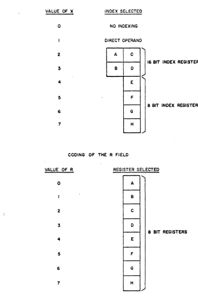
CODING OF THE X FIELD
VALUE OF X
o
2
3
4
5
6
7
INDEX SELECTED
NO INDEXING
01 RECT OPERAND
] 16 BIT INDEX REGISTERS
A C
B D
E
F
8 BIT INDEX REGISTERS
G
H
COOING OF THE R FIELD
VALUE OF R
o
2
3
4
5
6
7
REGISTER SELECTED
A
B
C
0
8 BIT REGISTERS
E
F
G
H
[image:26.617.105.506.75.695.2].",.
Figure 4-1. Register Selection
STR
STM
inforrnation transfe r to the corre sponding bits of R.
Timing: 2 IF X
I
I, I IF X=
IStore R
Store the character in register R into the specified mem-ory location.
Timing: 2
Store R through Mask
Store the character in register R into the specified mem-ory location through the rna sk in re gi ste r E. Ze roe s in
E inhibit change in the corresponding bits of the memory
location.
Timing: 2
2. Multiple-Character Transfer
1
, The following instructions permit the simultaneous transfer of
multiple-character groups between certain data registers. They
are useful for rapidly loading or unloading a group of registers.
The R field of these commands is utilized as an extension of the
Op Code.
BRL
BRH
STL
Bring to Low Registers
Bring fields CI, C2, C3 and C4 of the specified word in
memory to the low registers A, B, C and D respectively.
Timing: 2
Bring to High Registers
Bring fields CI, C2, C3 and C4 of the specified word in
memory to the high registers, E, F, G and H
re spectively.
Timing: 2
Store Low Registers
Store the characters in the ]0\\/ registers A, B, C and D
into the specified word in nlernory in fields CI, C2, C3
and C4 respectively.
Timing: 2
STH
BXA
BXB
SXA
SXB
Store High Registers
Store the characters in the high registers E, F, G and
H into the specified word in memory in fields GI, G2,
G3 and G4 re spectively.
Tirn ing: 2
Bring the right-most 16 bits of the specified word in
memory to the data registe r pair A, G de signated as
index register 2.
Timing: 2 IF X
I
1, 1 IF X=
1Bring the right-most 16 bits of the specified word in
memo ry to the data regi ste r pair B, D de signated as
index register 3.
Timing: 2 IF X
I
1 J 1 IF X=
1Store the data register pair A, G designated as index
register 2 in the right-most portion of the specified
word in memory.
Tinling: 2
Store the data register pair B, D designated as index
registe r 3 in the right-most portion of the specified
word in memory.
Tinling: 2
3. Characte r Arithmetic and· Conlpare
The se instructions will pe rfornl unsigned arithmetic ope rations
on a single 8 - bit field, 0 r will compare the content s of one of the
data registers with a specified character in core memory. All
characters are considered to be magnitudes, and subtraction
underflow will yield a difference in complement form.
ADD Add
Add the specified character in memory to register Rand
put the result in register R. Overflow sets the overflow
memo.
Tim ing: 2 IF X
I
1, 1 IF X=
1SUB Subtract
CCM
4. Logical
Subtract the character in memory from register Rand
put the result in register R. Underflow sets the
over-flow Inemo.
Timing: 2 IF X ~ 1, 1 IF X
=
1 Compare Character to MemoryThe character in register R is compared to the specified
character in menlory. If the register contents are
greate r than memory, the next sequential instruction is
executed. If the two characters are equal, one
instruc-tion is skipped. If the register contents are less, two
instructions will be skipped.
Timing: 2 IF X ~ 1, 1 IF X = 1 (add one if skip occurs)
The L-1192 logical operations enable t-Ietting and te sting any
com-bination of bits held in any of the data registers .
EOR
SCH
. Exclusive Or
Replace the specified character in memory with its
bit-by-bit exclusive-or with the contents of register R.
Timing: 2
Set Character
Set all selected bits of regi ste r R to one (U
=
1) or ze ro (U=
0). Selected bits are those which are masked bycorresponding ones in W. (I is not used.)
Tirning: 1
TSC Test Character
Test all selected bits of register R for values of one
(U = 1) or zero (U = O). Selected bits are those which
are masked by corresponding ones in W. A skip occurs
if (1) I = 1 and all selected bits match U, or if (2) 1=0 and a misn1atch exists.
Timing: 1 (add one if skip occurs)
TSP Te st Parity
5. Shift
Test all selected bits of register R for parity. Selected
bits are those which are masked by corre sponding one s
in W. A skip occurs if (1) I = 1 and parity is odd, or
(2) I
=
0 and parity is even. (U is not used.) Timing: 1 (add 1 if skip occurs)Single characters may be shifted within any of the data registers.
Shifting may be open or cyclic as specified. The number of
place s shifted may be modified by an index regi ste r. The shift
count (N) is contained in the right-most bits of the instruction.
A maximum of 8 shifts will be made.
SCL Shift Character Left
RCL
The contents on register R are shifted left the number
C?f place s specified by N. Bits shifted past the high
order end of the register are lost, and zeros replace
those shifted away from the low order positions.
Timing: (N -;- 4)
+ 1
Rotate Character Left
The contents of register R are shifted left the number
of place s specified by N in a cyclic manne r. Bits
leaving the high order end of the register are shifted
into the low orde rend.
Timing: (N
-+-
4)+
16.
Index ModifyDXR Decrement Index Register
The contents of the instruction R field (U
=
¢),
or the contents of the register specified by the R field issubtracted from the index register as specified by X.
If I =
¢,
the next sequential instruction will always bee xe cuted. If I = 1, the re sult of the de c re me nt will be
tested. If the decrement did not cause the index
regis-ter contents to pass through zero, the next instruction
is taken from the location specified by W. If the index
register did pass through zero, the next sequential
instruction is executed.
Timing: 1
IXR Increment Index Register
The contents of the R field or the register specified by
R, according to the setting of U, is added to the index
register specified by X. If I =
¢,
the next sequential will be executed. If I=
1, the results of the increment will be compared to W/e
of the instruction. If the index is gr'eater, or if it overflowed as a result of theincrement, the next sequential instruction will be
executed. Otherwise one instruction will be skipped.
Timing: 1
4.2 VARIABLE FIELD OPERATIONS
The se instructions facilitate the proce s sing of variable length characte r
fields as required, for example, by me ssage formatting and editing. This
capability is important in those applications providing message switching
on a mix of both synchronous and asynchronous communication channels.
It is also useful in formatting messages for magnetic tape, disc file,
and/or display equipment.
Variable field instruction execution permits each of two operand
addresses to specify independent field locations and lengths, up to a
maximum of 16 characters. The addresses of both operands are
sub-ject to normal modification through indexing and indirect addre ssing.
A separate register, designated the Field Operand Address Register
(FOAR), is provided to hold the address and length of the first operand.
The tinling for the execution of most field instructions is a function of the
nurnber of characters in each operand field (Fl and F 2 ), and to some extent the locations of word boundaries within these fields. If a
recom-plement cycle is required, additional time is required.
Variable field arithmetic operations may be perforlned on both.binary
and decimal operands. The sign of each operand is carried in the least
significant character field. These arithmetic operations are algebraic
and are executed in the following manne r:
Decilnal:
The four least significant bits of each character field contain the decimal
digit. Bit
6
of the least significant charactc r of each operand fieldcon-tains the sign. The remaining bits will be ignored. The address and
field length of operand 1 is in the Field Operand Address Register.
Operand 1 is added to or subtracted frorn operand 2, whose length and address is carried in the instruction word. The result of the operation is
stored in place of ope rand 2. The re suIt of the ope ration is in true sign
and magnitude form. If the result passes through zero, the ten's
comple-H1ent (recomplementing) of the result is taken. To yield meaningful
results, in the event the operand lengths are not the same, operand 2
n1ust have the greater length.
Binary:
The least significant bit of the lea st significant character of each ope rand
is considered to be the operand sign. Processing is similar to that
de-scribed for decimal operands above, and operand 2 must always have the
greate r length.
The in struction format for variable -field ope rations is similar to that
described for the standard single character commands. U and R in the
instruction word, however, specify a field length of up to
16
characters.The following instructions compri se the li st of variable field ope rations.
Timing is given in memory cycles.
IFO Initialize Field Ope ration
SFA
AFB
SFB
This instruction sets up the Field Operand Address Register
(FOAR). U and R are transferred directly to the FOAR.
The W
Ie
field relnains in the instruction register until the specified address IDodification has been completed, at whichtime W
Ie
is transferred to the FOAR. Except for the spe-cial case of the Compare Fields Equal instruction describedbelow, the FOAR 111USt be initialized each time before
another variable field operation is performed.
Timing: 1
Store Field Address
The contents of the FOAR are stored in U, R, and W
Ic
of the specified memory location. The R field of theinstruc-tion is a part of the operainstruc-tion code.
Timing: 2
Add Field Binary
The two binary operands whose addresses are specified by
the FOAR (operand I) and W
Ic
of the instruction (operand 2) are added algebraically.' The results of the additionoccu-pies the position of the second operand. The result will
carry true sign and Inagnitude. Overflow will set the
over-flow memo.
Tirning: (a) No recomplen1ent cycle: 3.25
+ .75 F2
(b) Recomplement cycle: 4
+ F2
Subtract Field Binary
The two binary operands whose addresses are specified by
FOAR (ope rand l) and W
Ie
of the instruction (ope rand 2) are subtracted algebraically. The results of the subtractionoccupies the position of the second operand. The result
will carry true sign and magnitude. Underflow will cause
the overflow memo to be set.
Timing: (a) No recornplement cycle: 3.25
+
.75 F2(b) Recomplement cycle: 4
+ F 2
AFD
SFD
CFE
CFM
Add Field Decinlal
The two de cimal operands whose addre s se s are specified by
FOAR and W
Ic
of the instruction are added algebraically. The surn is stored in the location of the second operand, andcarries true sign and magnitude. Overflow will set the
over-flow memo.
Tirning: (a) No recol11pleluent cycle: 3.25
+ .75 F2
(b) Recornplement cycle: 4
+
F 2 .Subtract Field Decimal
The two decimal operands whose addresses are specified by
FOAR and W
Ic
of the instruction are subtracted algebrai-cally. The diffe rence ~n stored in the location of the second operand, and carries true sign and magnitude. Underflowwill set the overflow luemo.
Timing: (a) No recomplement cycle: 3.25
+ .75 F2
(b) Recomplement cycle: 4
+ F 2
Cornpar'e Fields Equal
This instruction compare s the two fields whose addre sse s
are specified by FOAR and W
Ic
of the instruction. The field lengths are as sumed to be identical and the lengthcount in FOAR will be ignored. Comparison is on a
bit-by-bit basis. Equal cOlnparison causes the next sequential
instruction to be executed. Unequal comparison will cause
one instruction to be skipped. Since FOAR need not be
initialized before each execution of CFE, automatic indexing
through a table of contiguous entries may be achieved
with-out the use of index registers.
Timing: (a) No skip: 2.5
+
5 F Z(b) Skip: 3. 5
+ . 5 F 2
Compare Field Magnitude s
The operands whose addresses are specified by FOAR and
W
Ic
of the instruction are compared arithmetically withMFM
signs treated as part of the rnagnitude. If the ope rand
ad-dressed by FOAR is greater than or equal to the operand
specified by W
Ie
of the instruction, the next sequential in-struction will be executed. If not, one inin-struction will beskipped. The two operands used with CFM need not have
identical lengths.
Timing: (a) No skip: 2.5
+ .5 F2
(b) Skip: '3. 5
+ .5 F2
Move Field in Memory
The field whose address is specified by FOAR is moved to
the addre s s specified by W
Ie
of the instruction starting in lowe r mernory. Reaching the end of the shorte r field willte rminate the operation.
Timing: 2.5
+
.5 (FI , F 2 ) min.4.3 FULL WORD OPERATIONS
The word instructions provide full-word (32 bit) transfer, arithmetic,
and logical ope rations.
The format for most of these instructions is as follows:
6 1 3 1 3 1 6
0 P
eo
DE Ut
..I
I X W)
.. , " "
The eight character registers A, B, . . . , H are not modified by 2
word arithmetic. Fields I, X and Ware still employed to specify the
location of the second ope rand. Load and Store word instructions use the
one-bit U field to specify one of two one-word registers, Rand Q. r'\.
third but non-addressable register also participates in word operations.
Word operands are 32 bit numbers, with negative numbers represented
in 2' s complement form. The tirning for the following word instructions
is given in memory cycles.
1
WAD
WSB
WMP
WDV
WCM
Word Add
Add the specified word in lnemory to R and put the,re suIt
in Inemory. Ove rflow sets the ove rflow memo. Q is
unchanged.
Timing: 2
Word Subtract
Subtract the specified word in memory from R and put the
re sult in memory. Underflow sets the overflow memo.
Q is unchanged.
Timing: 2
Word Multiply
Multiply the specified word in memory by R, and put the
most significant half of the product in R and the least significant half of the product in Q. The sign of the least
significant half is made the senne as that of the most
signi-ficant half.
Timing: 6.25
Word Divide
Divide the specified word in n1emory into R & Q and put the
quotient in Q. The remainde r is placed in R in twos com-plement form.
Timing: 10.5
Word Compare
The word in R is compared to the specified word in
mem-0ry. If the register contents are algebraically greater
than the word in memory the next sequential instruction is
executed. If the two words are equal, one instruction is
skipped. If the register contents are less than the word
in memory, two instructions are skipped.
Tim'ing: (a) No skip: 2
(b) Skip: 3
WBR
WST
WCD
WSF
WSL
Word Bring
Bring the specified word in memory to register R (U
=
~) or re gi ste r Q (U = 1).Tin1ing: 2
Word Store
Store the word in register R (U
=
¢)
or register Q (U=
1) into the specified mernory location.Timing: 2
Word Complement
Two's complement the contents of the R register.
Tirning: 1
Word Shift
Shift the word in register R (U
=
¢)
or register Q (U=
1) right (I =¢)
or left (I=
1), the number of places specified by the rightmost five bits of the instruction. Signs arenot included, overflow digits are discarded. Indexing of
the number of places shifted may be modified by indexing.
Timing: 1.5
+ .25N
Word Shift Long
Shift the combined words in register Rand Q right (I
=
¢)
or left (I = 1), the number of places specified by the right-mo st six bits of the instruction. Signs are not included,overflow digits are discarded. The number of places
shifted may be modified by indexing. Tinling: 1.5+.25N
4.4 PROGRAJ'v1 CONTROL OPERATIONS
NOP No-Ope ration
Proceed with next instruction. (Op code field used only. )
Timing: 1
JMP Jump
Take the next instruction from memory location Was
modified by X and I. (R and U are not used.)
Tilning: 1
JSL JUlnp and Store Location
HLT
The location of this instruction plu s one are stored in the
Inemory location specified by W. The next instruction is
taken frorn location W
+
1. Only the word address inloca-tion W is affected. Remaining posiloca-tions are left unchanged.
Tirning: 2
Halt
Execution of this instruction halts the compute r program
by removing the RUN condition. Depressing the PROGRAM
STAR T pushbutton on the operators console re starts the
progranl with the instruction specified by the program
counter. (Op code field used only.)
Timing: 1
4.5 INTERNAL CONDITION OPERATIONS
The L-1192 has a nurnber of internal condition indicators, which may be
te sted and modified.
Inte rrupts
The interrupts are enabled through the use of a mask, which may be stored
anywhere in core memory. The bits within this mask correspond to the
various interrupt conditions. By enabling interrupts from this mask, only
the desired interrupts nlay be used.
ESI Enable System Interrupts
The word at location W is used as a mask to enable
inter-rupt operation for the I/O Interface specified by R, U.
For every position which contains a one, the corresponding
interrupt will be enabled. For every position which
con-tains a zero, the corresponding interrupt will be disabled.
Timing: 2
Systcnl Conditions
System conditions may be set or reset, and tested for on or off condition.
The available instructions utilize the W
Ic
field to select the memo or condition to be set or tested. This memo or condition is thereforesub-ject to index register modification.
SSC Set System Condition
Tee
For those conditions which can be switched by prograln,
this instruction will cause the s tate of the addre s sed device
to be equal to the status of the U bit. Thus, if the U bit is
zero, the device will be reset. If U is one, the device will
be set. If this instruction is addre ssed to a device which
is not program settable, it will execute as NOP.
Timing: 1
Te st Control Condition
The condition of the specified memo or switch is compared
to the U bit. If the condition and the bit are equal, the
next sequential instruction will be executed. If not equal,
one instruction will be skipped.
Timing: 1
4.6 COMMUNICATION INTERFACE OPERATIONS
Input-output character transfers for the C0111nlUnication channels and the
slow-speed on line devices (paper tape, punched card, and type\vriterl
printer) provide interlaced core 111emory aCCC:-iS to permit simultaneous
operation.
Due to frequency of se rvicing the DDL inte rface, instructions are
pro-vided which greatly reduce the proce ssing load when removing data froin
the low and high priority channel activity table s (CAT 1, CAT 2). In a
single instruction a re com bined the functions of te sting for the pre sence of
data in CA T 1 or CA T 2, bringing the next entry to be proce ssed to the
data registers if data is waiting to be processed, and moving hardware
bookkeeping markers to the next entry to be processed.
When either ICH or ICL is executed, the relative positions of the load and
unload 111arkers are tested. If the SalTIC, indicating the tested table is
empty, the instruction terminates and the next sequential instruction is
executed. If the markers are not the same, the entry at the location of
the unload marker (VI, V2) is brought into the data registers as shown:
Character E Register
Channel Ident~ty F Registe r
I/O Indicator G Register
The unload marker is then stepped cyclicly to the next entry position in
the table. The next sequential instruction is skipped and this instruction
is terminated.
The format for the ICH and the ICL instructions is:
6
24Op Code
ICH Initiate High Priority Characte r Cycle
The relative positions of Ll and VI are tested. If equal,
the current instruction te rminate s and the next instruction
In sequence is executed. If not identical, the next entry
in CAT I is obtained from the location specified by VI.
The next sequential instruction is skipped and VI is
autolTIatically stepped.
Tim i ng: I IF L 1
=
V I, 2 IF L 1I-
V 1,
ICL Initiate Low Priority Character Cycle
The relative positions of L2 and V2 are tested. If equal,
the current instruction te rminate s and the next sequential
instruction is executed. If unequal, the next entry is
acce ssed from CA T 2 at the location specified by U2.
U2 is stepped, the follo\ving instruction is skipped, and
the current instruction is terminated.
Tirning: 1 IF ,L2 = U2, 2 IF L2
f.
U2The ECH and the DCH instructions control the operation of the DDL
inter-face module scanner. The instruction fornlat is:
ECH
DCH
6 1 3 22
Op Code R
.. .;i!
Enable Channel
The interface module attached to scanner position R
(one of eight positions) is placed in operation.
Charac-te r s will be automatically input or output unde r control
of the Line Unit Inte rface module or Low Speed I/O device.
Timing: 1
Disable Channel
The interface module attached to scanner position R (one
of eight positions) is taken out of operation. Any fragment
of a character in transmission will be lost.
Timing: 1
4.7 INPUT/OUTPUT OPERATIONS
The L-1192 Controller Processor may interface with up to sixteen I/O
Channel s. Each channel added to the sy stem contains the required
con-trol logic plus a Command Regi ste r and a Block Concon-trol Regi ste r, and
can cOlnmunicate with up to 16 peripheral devices.
For the purpose of the following discussion, the term "instruction" refers
to those 9perations which are decoded and executed in the instruction
register. The term Ilcommand" designates those operations which are
executed in the I/O interface. To activate most input/output operations,
it is necessary for the L-1192 program to initiate an
no
instruction,\'vhich selects one of sixteen interface channels and specifics the location
of a CorTI1TIand Word. If the designated interface is busy, the Program
Counter lTIOVe s to the next instruction in sequence following the lIO. If
the inte rface is not busy, the C0l111TIand Word and a following Block
Con-tr01 Word are transferred to the selected I/O Interface. The Command
Word, which specifies one of several available I/O commands and
selects an I/O device, is transferred to the interface Command Register.
The C0l11mand Word in core memory must be followed by a Block Control
Word. It specifies the data transfer starting memory address and the
required character count, which are loaded'into the interface Block
Con-trol Register. Input/output operation then proceeds and overlaps
com-pute r instruction acce s s and execution. The Program Counte r returns
the internal program to the address of the 110 instruction plus 2. A flag is set when the I/O transfer is completed, which will provide a program
interrupt unless the indicator is n1asked.
A single interface transfer can proceed at one time on any I/O Channel.
Multiple and simultaneous input-output operations therefore require more
than one channel.
The parameters contained in the interface rpgisters may be accessed by
rneans of a Save I/O Register instruction. A IJalt I/O instruction also
pe rmits the program to immediately te rminate any I/O transfe rope
ra-tion when required. These two instrucra-tions need not be preceded or
activated by an 110 instruction.
The following paragraphs provide a description and present the formats for
the I/O instructions and commands.
lIO Initiate I/O Ope ration
6
4 1 316
2Op Code
U,
R I X WI
U, R These 4 bits select oneof
16
Interfaces (I/O Channels) to beplaced in operation, unless already busy.
I Indirect Bit
x
Index specification. X=
1 has no meaningW This address, lTIodified by I and X specifies the core
mem-ory location of the Comrnand Word.
Command Word Format
2 4 10 16
DS
o
DS Device Selection. This field specifies one of sixteen devices
on the selected interface.
o
Device Operation Code. This field specifies the input/outputcommand to be executed. The translation between the
de-vice ope ration code and the actual dede-vice function controls
will be largely 'done by the device adapter.
Block Control Word Format
2 12 18
Block Length Sta rting Add re s s .
1 . Starting addre ss can be any character position in memory.
2. Block length can be as great as 4096 characters.
SIO Save I/O Registers
4
Two words, as described below, are transferred frorn
the interface specified by R, U to core memory at the
location specified by W /C.
Timing: 3
10 18
Device Device
~
Operation
I
Addre ss
Code
Device Current
Condi tions Data Address
14 18
HIO Halt I/O Ope ration
The e?Cecution of thi s instruction will cause the inte rface
specified by R, U to terminate operations immediately.
The contents of the interface Block Control Register and
the inte rface Command Regi ste r will be de stroyed by thi s
instruction.
Timing: 1