A High Speed Explicit Pulsed Dual Edge
Triggered D Flip Flop
Manan Joshi
IIMT COE, Gr. Noida India
D.S.Chauhan
UTU, Dehradun
India
B.K.Kaushik
IIT, Roorkee India
ABSTRACT
This paper presents an efficient explicit pulsed static dual edge triggered flip flop with an improved performance. The proposed design overcomes the drawbacks of the dynamic logic family and uses explicit clock pulse generator approach to achieve dual edge triggering. The proposed flip-flop is compared with existing explicit pulsed dual edge triggered flip-flops. Based on the simulation results overall improvements of 12.67% and 10.15% are observed in delay and power delay product respectively.
General Terms
VLSI, optimisation, explicit pulse generator, embedded logic, clock network.
Keywords
Power delay product, flip flop, power consumption, propagation delay, CMOS logic, transmission gate, explicit pulsed.
1. INTRODUCTION
Flip Flops and latches form part of clock distribution network, timing elements, memory etc in digital systems. Reducing delay and power consumption will have a deep impact on the performance of digital systems. Flip Flops affect the clock frequency, since their delay occupies a significant fraction of the clock cycle, especially in fast micro-architectures with low logic depth. Together with the circuits devoted to the clock generation and distribution, Flip Flops are part of the clock network that is responsible for 30%-50% of the whole chip energy budget [1]. Power consumption has become a significant issue in modern IC designs, especially for high-end processors and energy-aware mobile devices.
During recent past a lot of advancements have been observed in the field of Flip Flops. The earliest work on edge triggered D-Flip Flop gives the Yuan-Svensson D-Flip Flop [2] that was proposed in the year of 1996. The transistors in this flip flop have conflicting requirements and hence this circuit cannot be optimised well. The sense amplifier based flip flop [3] consisting of a sense amplifier and slave latch is very similar to a master slave flip flop. Here only one transistor is active during clock transition that increases the driving capability of the output stage and reduces power dissipation. But being a two stage, circuit it cannot reduce delay efficiently. The conditional capture flip flop [4] is an innovation where the internal nodes switch only when the output needs to be switched. This approach can save power dissipation in a circuit. Another flip flop introduced has the advantage of being able to avoid stacking of PMOS transistors. As a consequence, low voltage and low power operation becomes feasible. The low swing clock double edge triggered flip flop [5] uses a data sampling front end and a data transferring back end and the internal nodes switch only when there is a data
change. It results in reduced power consumption. Conditional discharge flip flop [6] introduced another innovation where output switches off the discharge path of first stage to prevent it from discharging and doing evaluation in succeeding clock cycles as long as the input does not change. Thus the flip flop reduces power consumption further. The conditional precharge flip flop was also introduced to save power consumption by not allowing precharging to take place as long as D and Q have similar input and output respectively. Similarly the conditional data mapping flip flop [7] reduces the dynamic power consumption by mapping the inputs to a configuration that eliminates redundant internal transitions. The data mapping is conditional i.e. when the applied input is the same as the output that results in no internal transitions. A clock branch sharing flip flop [8] reduces the number of clocked transistors and thus reduces the power consumption. In clocked Pseudo NMOS level conversion flip flop [9], Pseudo NMOS has been used for conditional discharge. The benefits of level conversion are also used. The energy efficient dual edge triggered level converting flip flop [10] has the benefits of level conversion and data retention in sleep mode that are used to reduce switching activity and hence power consumption.
The design of the proposed D Flip Flop uses both Transmission gate Logic as well as CMOS logic styles in such a way that it not only reduces the number of transistors used but also the drive capability that in turn reduces delay.
This paper introduces a new dual edge triggered Flip Flop using CMOS logic, transmission gate and pulse generator. This architecture is capable of embedding logic functions [19] and can be used for designing control units and pipelined datapath structures. It also performs charge sharing free operation more efficiently. This dual edge triggered flip flop that uses the clock pulse based approach reduces power consumption drastically in comparison to earlier reported research works [12-14]. The proposed flip flop avoids MOS transistor stacking, reduces internal node switching and as a
consequence low voltage and low power operation is possible. The two stages i.e. the input stage and the output stage are basically CMOS inverters that switch only when there is a data change and hence result in reduced power consumption. The pass transistors, NMOS and PMOS are used to construct the transmission gate that provides edge triggering. It results in reduction of the number of clocked transistors and power consumption.
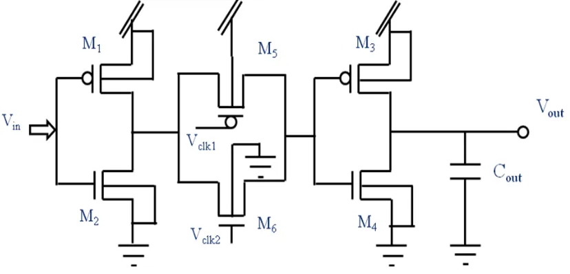
[image:2.595.91.505.229.428.2]The rest of the paper is organised as follows. Section II presents the proposed D Flip Flop with its functionality. Section III gives the Simulation Set-up used. Section IV compares the proposed D Flip Flop with architectures proposed earlier [12-14]. Finally, conclusions are drawn in section V.
Fig 1: Proposed Dual edge triggered Flip Flop
2. THE PROPOSED FLIP FLOP
The proposed D Flip Flop shown in Figure 1 consists of an input and output stage that is an inverter, whereas the middle stage that allows the input to pass through only at the clock edge. The two inverters invert the signal twice and hence the output is the same as input. Two clock pulses that are generated from pulse generator are applied to the MOSFETs (M5 & M6). The parasitic capacitance at the input of the output
stage inverter holds the charge/signal. The NMOS (M6) serves
as a good pull down device and brings the input of the output stage inverter to zero volt, whereas the PMOS (M5) serves as a
good pull up device and brings the input of the output stage to Vdd. The Figure 1 above shows the proposed D Flip Flop and
Figure 2 ahead shows the clocks. In Figure 1 clock Vclk1 is
generated from Vclk2 by passing it through an inverter.
The clock Vclk2 is generated from the clock with 50 percent
duty cycle using an explicit pulse generator shown in Figure 3. The explicit pulse generator produces a pulse at every clock edge (Vclk2). The three inverters serve to delay the clock pulse
applied at input of the XNOR gate and provide complementary inputs. When Vclk switches from low to high
or vice - versa the inputs to the XNOR gate are momentarily same. Otherwise the two inputs are complementary in nature. This produces a pulse at every clock transition. It is essential to ensure that inverters I1 &
I2 delay the effect of change in clock edge. This is achieved by
increasing the length (L) of the NMOS and thereby weakening it so that its turn ON is delayed. When length (L) increases the resistance increases allowing NMOS to remain OFF for a longer time. The inverter also will have a longer falling edge delay. Vclk2 is generated at node X.
The clock pulses shown in Figure 2 are derived from the explicit pulse generator. Figure 3 shows the circuit of the pulse generator. These pulses are applied to the transmission gate formed by M5 and M6 as shown in Figure 1 causing edge
triggering. Power consumption of a particular clocking scheme can be represented as [5]
Pclk-scheme = Pclk-network + PFF (1)
where Pclk-network and PFF represent power consumptions in the
clock network and flip flops respectively. The total power dissipation of the clock network depends on both the clock frequency and the data rate that can be expressed as [11].
Pclk-network = Vdd2[ fclk(Cclk + Cff,.clk) + fdata Cff.data]
(2)
where fclk , fdata , Cclk , Cff,.clk , Cff, data represent the clock
Fig 2: Clocks applied to proposed D Flip Flop
PFF = {(αi. Ci. γ + αo. Co. γ + Cclk-buf).Vdd2 (3)
where Ci , Co , αi , αo , Cclk-buf is the internal node capacitance
of the FF, the output node capacitance of the flip flop, the internal node transition activity ratio, the output node transition activity ratio, the capacitance of the clock buffers repectively. γ is 2 for double edge triggered flip flops and 1 for single edge triggered flip flops.
From the above expression (2) it is obvious that the clock power can be reduced if any of the parameters can be reduced. The reduction of Vdd is already the trend of contemporary
design and has the strongest impact on the Pclk-scheme
expression. By reducing the overall capacitance of the clock network, the power dissipation is reduced. Similarly, by reducing the capacitance inside a flip flop, Cff.clk and Cff,.data,
power is reduced.
From the expression (3) it is clear that power dissipation in the flip flop is reduced if any of the parameters in the expression is reduced. The internal node capacitance is reduced by keeping the number of nodes as less as possible and keeping the dimensions of the MOSFETs as small as possible. The internal node transition activity αi and output node transition
activity αo is reduced by designing the circuit in such a way
that the internal and external nodes switch only when the data change takes place.
Fig 3: Circuit showing explicit pulse generator
The conclusions from the above three expressions are used while designing the proposed Flip Flop. Attempt is made to keep the MOSFETs M3, M4, M5 and M6 as small as possible
[image:3.595.331.524.367.524.2]to reduce power consumption in the data path network. Moreover the design of the Flip Flop is such that the internal nodes switch only when the data change takes place and hence αi and αo are reduced.
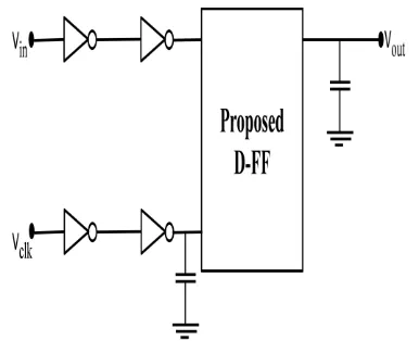
Fig 4: Set up used for simulation
3. SIMULATION SETUP
The set-up used in our simulations is as shown in the Figure 4. The circuits are simulated in real environment, where the buffers (inverters) drive the flip flop inputs (data and clock) and the output drives a capacitive load of 21fF. An additional capacitance of 3fF is placed after the clock driver. We have applied at the D input, an input data with an activity factor of 25% to reflect the average power consumption. Power consumed in the data and clock drivers is included in our measurements. Clock frequency used is 125 MHz.
4. RESULTS AND DISCUSSIONS
[image:3.595.53.276.547.734.2]Table 1.Comparing the flip flops in terms of delay, power consumption and power delay product
Design Name
Tran count
DQ Delay
(ps)
Power (W)
PDP (fJ)
% change
in PDP SCDFF 29(17) 234.5 41.97 9.8 - DEPFF 29(14) 230.2 37.05 8.53 12.95 SEDNIFF1 29(11) 217.7 34.44 7.49 12.19
Proposed 22(6)2 190.1 35.42 6.73 10.15
1FlipFlop proposed in [12]
2In parenthesis is the transistor count of its latch
The primary drawback of flip flop SEDNIFF is that it is composed of twenty nine transistors out of which eleven are in the latch. The pulse generator has eighteen transistors that
continuously switch with clock. This results in higher average power dissipation. The pulse generator and the latch consist of stacked transistors that reduce the efficiency of the flip flop. In the proposed Flip Flop pass transistors that are used to construct the transmission gate have length (L) and width (W) that are sized to reduce delay. The inverter at the output also has optimum sized transistors [18] so that pass transistors and the transistors of the input inverter have W and L as small as possible. Moreover the pulse generator consists of sixteen transistors and the latch part consists of six transistors. This results in lower average power dissipation. Due to symmetry, scaling of the proposed flip flop is simple. Proper design of the pulse generator ensures low power consumption. To convert this flip flop into a latch a keeper transistor is required at the output.
A waveform of D making a 0
1 and 1
0 transition.Fig 5: Output of proposed Flip Flop Vout
5. CONCLUSION
This paper presented the design of a new explicit pulsed double edge triggered D Flip Flop. This flip-flop has reduced redundant switching and short current and hence reduced power consumption. The flip flop has least number of clocked transistors and lowest power consumption and is therefore suitable for use in high performance and low power environments. In addition to this, it is also capable of embedding logic functions and performs charge sharing free operation more efficiently.
6. REFERENCES
[1] N. Nedovic, and V. G. Oklobdzija, “Dual Edge Triggered Storage Elements and Clocking Strategy for Low Power Systems,” IEEE Trans. VLSI Systems, vol. 13, no. 5, pp 577-590, May 2005.
[2] Q. Huang, and R. Rogenmoser, “Speed Optimisation of Edge-Triggered CMOS Circuits for Gigahertz Single-Phase Clocks,” IEEE J. Solid-State Circuits, vol. 31, no. 3, Mar. 1996.
[3] B. Nicolic, V. G. Oklobdzija, V Stojanovic, W. Jia, J. K. S. Chiu, and M. M. T. Leung, "Improved Sense-Amplifier-Based Flip Flop: Design and Measurements,” IEEE J. Solid-State Circuits, vol. 35, no. 6, June 2000. [4] B. S. Kong, S. S. Kim, and Y. H. Jun,
“Conditional-Capture Flip Flop for Statistical Power Reduction,” IEEE J. Solid-State Circuits, vol. 36, no. 8, Aug. 2001. [5] C. Kim, and S. M. Kang “A Low Swing Clock
Double-Edge Triggered Flip Flop”, IEEE J. Solid-State Circuits, vol. 37, no. 5, May 2002.
[6] P. Zhao, T. K. Darwish, and M. A. Bayoumi, “High-Performance and Low-Power Conditional Discharge Flip Flop,” IEEE Trans. VLSI Systems, vol. 12, no. 5, May 2004.
[7] C. K. The, M. Hamada, T. Fujita, H. Hara, N. Ikumi, and Y. Oowaki, “Conditional Data Mapping Flip Flops for Low Power and High Performance Systems,” IEEE Trans. VLSI Systems, vol. 14, no. 12, Dec. 2006. [8] P. Zhao, J. M. Neely, P. Golconda, M. A. Bayoumi, R.
A. Barcenas, and W. Kuang, “Low Power Clock Branch Sharing Double Edge Triggered Flip Flop,” IEEE Trans. VLSI systems, vol. 15, no. 7, July 2007.
[9] P. Zhao, J.B. McNealy, P. K. Golconda, S. Venigalla, M. A. Bayoumi, W. Kuang, and L. Downey, “Low Power Clocked Pseudo NMOS Flip Flop for level Conversion in Dual Supply Systems,” IEEE Trans. VLSI Systems, vol. 17, no. 9, Sept. 2009.
[10]L. Y. Chiou, and S. C. Luo, “Energy Efficient Dual Edge Triggered Level Converting Flip Flops with Symmetry in Setup Times and Insensitivity to Output Parasitics,” IEEE Trans. VLSI Systems, vol. 17, no. 11, Nov. 2009. [11] M Alioto, E Consoli, and G Palumbo, "Analysis and
Comparison in the Energy-Delay-Area domain of nanometer CMOS flip flops: Part II - Results and Figures of Merit," IEEE Trans. VLSI Systems, vol. 19, No. 5, May 2011.
[12] X. X. Wu, and J. Z. Shen, "Low power explicit-pulsed triggered flip flop with robust output," Electronic Letters, vol. 48, no. 24, Nov. 2012.
[13] M.W. Phyu, W. L. Goh, and K..S. Yeo, "A low-power static dual edge triggered flip–flop using an output-controlled discharge configuration," IEEE Int. Symp. on Circuits and Systems, Japan, May 2005, Vol. 3, pp. 2429–2432.
[image:4.595.87.513.251.340.2][15] N. Lotze, and Y Manoli, "A 62mV 0.13µm CMOS Standard-Cell-Based Design Technique using Schmitt Trigger Logic," IEEE J. Solid-State Circuits, vol. 47, no. 1, Jan. 2012.
[16] S. Lutkemeir, T. Jungeblut, H. K. O. Burge, S. Aunet, M. Porrmann, and U. Ruckert, "A 65nm 32b Subthreshold Processor with 9T multi Vt SRAM and
adaptive supply voltage control," IEEE J. Solid-State Circuits, vol 48, no 1, Jan 2013.
[17] W. Chung, T. Lo, and M. Sachdev, “A Comparative Analysis of Low-Power Low Voltage Dual-Edge Triggered Flip Flops,” IEEE Trans. VLSI Systems, vol. 10, no. 6, Dec. 2002.
[18] R. Zimmermann, and W. Fichtner, “Low Power Logic Styles: CMOS versus Pass-Transistor Logic,” IEEE J. Solid-State Circuits, vol. 32, no. 7, pp. 1079-1090, July 1997.
[19] O. Sarbishei, and M. M. Nejad, “A Novel Overlap based Logic Cell: An Efficient Implementation of Flip Flops with embedded Logic,” IEEE Trans. VLSI Systems, vol. 18, no. 2, Feb. 2010
[20] J. B. A. Constantino, and J. A. R. Madamba, "Static dual edge flip flop implementations on the 90nm process," in Proc. IEEE 2011, 5th Asia Modelling Symp.