Influence of the doping of the absorber and the charged
defects on the electrical performance of CIGS solar cells
SOCE Mouhamadou Mamour
*, DIENG Moustapha
**, EHEMBA Alain Kassine**, DIALLO Demba**, WADE
Ibrahima**
*
Laboratory of semiconductor and Solar Energy; Physics Department, Faculty of Science and Technology University CHEIKH Anta DIOP, DAKAR-SENEGAL
**
Laboratory of semiconductor and Solar Energy; Physics Department, Faculty of Science and Technology University CHEIKH Anta DIOP, DAKAR-SENEGAL
Abstract- In this paper, we have tried to show the importance of doping and defects charged on CIGS solar cells. Indeed according to our simulations, we could see that the electrical performance of these types of cells highly dependent on these two parameters. We also studied the dependence between doping and charged defects on the evolution of the electrical parameters. It was found that the results with neutral defects different from those charged with defects. The doping level for best performance (solar cell with Cu-poor absorber) is lowest with neutral defects than with the charged defects.
Index Terms- charged defect, CIGS, Cu-rich, Cu-poor, Doping.
I. INTRODUCTION
Solar cells based on Cu(In,Ga)Se2 are currently the best thin film solar cells and are the only devices capable to rich photovoltaic conversion efficiencies near 22% [1]. This tells us about the future of these cell types, and improvement which it is subject. In these cell types, the absorber is the central element, and has several features whose final performance cell depends. First, defects that are either superficial or deep. Superficial defects may be linked to the doping of these materials and deep defects are often charged statements that are donors, acceptors or neutral.
Doping is very important in semiconductor materials. It strongly influences the efficiency. In the case of our study, doping CIGS is due to intrinsic defects: meaning the shortcomings and deficiencies of copper or selenium. The first type of gap will lead to a p-type material, and the second to n-type material. [2]
So far CIGS solar cells with doped p-type absorber give a higher yield. In reality, this corresponds to the Cu-poor material. In various studies, they found that doping varies depending on the copper content in the material. Thus the Cu-rich absorber will be much doped but will have a lower efficiency caused by the recombination at the interface absorber / buffer layer [3].
In the following we will try to model and simulate the observations using SCAPS.
First we will do the simulation of a solar cell with different doping concentration of the absorber but considering the deep flaws as neutral (which do not exist in reality) and then consider the case or deep defects will charged.
II. MODELING USING SCAPS
Our model is based on CIGS Numos Baseline SCAPS but with some modifications. We will vary the doping 1014 to 1018 cm-3 and see the evolution of the electrical parameters. We will consider two cases: the first WERE defects are considered neutral, and the second defects will be charged. All simulations are performed at a temperature of 300 K. Illuminated characteristics have been simulated under AM1.5G illumination conditions with a power density of 100 mW/cm2.
1. PRESENTATION SCAPS
The terms of current density Jn et Jp are respectively given by equations (4) and (5) when the tunnel effect is not consider; if not other terms can be added.
𝐽𝑛 = −𝜇𝑛𝑛
𝑞
𝜕𝐸𝐹𝑛
𝜕𝑥 (4)
𝐽𝑝 = +𝜇𝑝𝑝
𝑞
𝜕𝐸𝐹𝑝
𝜕𝑥 (5)
2. WITH NEUTRAL DEEP DEFECTS.
Table 1 shows our simulation parameters. Table 2 gives the properties of the interface p-Cu (In, Ga) Se 2 / n-CdS and different layers.
Tableau 1: Cu (In, Ga) Se 2 Solar Cell Parameters
Parameters p-Cu (In, Ga) Se2
Absorber n-CdS Buffer i-ZnO Window n-ZnO Window
d [nm] 3000 50 50 200
εr 13.6 10 9 9
χ [eV] 4.5 4.2 4.45 4.45
Eg [eV] 1.1 2.4 3.3 3.4
νn [cm/s] 107 107 107 107
νp [cm/s] 107 107 107 107
µN [cm2/Vs] 100 100 100 100
µP [cm2 /Vs] 25 25 25 25
|NA-ND| [cm-3] 1014 ; 1015;1016 ; 1017 or 1018 1017 1018 1018
Tableau 2: Bulk Defect and Interface Properties
p-Cu (In,Ga)Se2 Absorber
Interface n-CdS
Buffer
i/n-ZnO Window
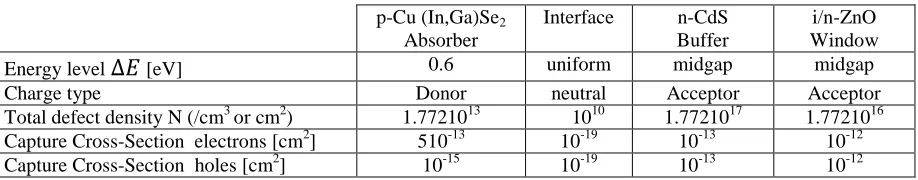
Energy level ∆𝐸 [eV] 0.6 uniform midgap midgap
Charge type neutral neutral neutral neutral
Total defect density N (/cm3 or cm2) 1.7721013 1010 1.7721017 1.7721016
Capture Cross-Section electrons [cm2] 510-13 10-19 10-13 10-12
Capture Cross-Section holes [cm2] 10-15 10-19 10-13 10-12
3. WITH CHARGED DEEP DEFECTS.
[image:2.612.74.533.634.724.2]To show the influence of the charge of deep defects, we will make the simulation by changing the types of charge and always varying the doping level of the absorber of 1014-1018 cm-3. Table 1 will be unchanged against for Table 2 type’s charges will be amended and give the table 3.
Table 3: Bulk Defect and Interface Properties
p-Cu (In,Ga)Se2 Absorber
Interface n-CdS
Buffer
i/n-ZnO Window
Energy level
∆𝐸
[eV] 0.6 uniform midgap midgapCharge type Donor neutral Acceptor Acceptor
Total defect density N (/cm3 or cm2) 1.7721013 1010 1.7721017 1.7721016
Capture Cross-Section electrons [cm2] 510-13 10-19 10-13 10-12
III. RESULTSANDINTERPRETATION
1. WITH NEUTRAL DEEP DEFECTS
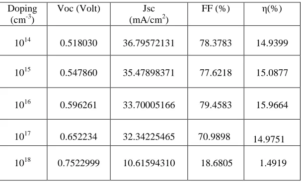
[image:3.612.156.459.175.359.2]From Tables 1 and 2, we get the results on some electrical parameters namely: the open circuit voltage Voc (V), the short circuit current Jsc (mA / cm2), the fill factor FF (%) the efficiency η (%). These results are shown in Table 4.
Table 4: Results of simulations in to doping absorber with defects neutrals.
Doping (cm-3)
Voc (Volt) Jsc
(mA/cm2)
FF (%) η(%)
1014 0.518030 36.79572131 78.3783 14.9399
1015 0.547860 35.47898371 77.6218 15.0877
1016 0.596261 33.70005166 79.4583 15.9664
1017 0.652234 32.34225465
70.9898 14.9751
1018 0.7522999
10.61594310
18.6805 1.4919
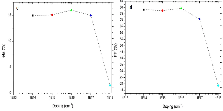
Figures 1 (a), 1 (b) and 2 (c), 2 (d) respectively show the changes in the open circuit voltage, short circuit current, the fill factor and the efficiency according to doping. In Figure 1 (a) there is an increasing trend of Voc depending on the doping of the absorber. The Cu-rich absorbers are more doped than the Cu- poor absorbers.
Figure 1: Variation of Voc (a) and the Jsc (b) according to doping.
Indeed a strong doping implies a value of Voc most important, this tells us about the interest of doping of the absorber on the electrical performance of CIGS solar cells. The transport properties of recombination are better in the Cu-rich absorber, which should give a cell with rich absorber Cu much more efficient [3].
cell.
Figure 2: Variation of efficiency η (%) (c) and the fill factor FF(%) (d) according to doping.
2. WITH CHARGED DEEP DEFECTS
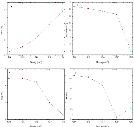
In this part, we have done the simulations considering the deep defects as charged. Table 3 was used. The results are shown in Table 6.
Table 6: Results of simulations in to doping absorber with charged defects.
Doping (cm-3)
Voc (Volt)
Jsc (mA/ cm2)
FF (%) η (%)
1014 0.522790 37.00283318 63.1109 12.2086
1015 0.554241 35.59585529 61.8635 12.2048
1016 0.610461 33.72192436 53.6887 11.0523
1017 0.705010 31.38062396 22.3044 4.9345
1018 0.790470 5.22898026 31.3583 1.2962
[image:4.612.159.456.433.606.2]Figure 3: Variation in electrical parameters according to doping: Voc (a); Jsc (b); η (c); FF (d).
Here, the best efficiency is obtained for doping between 1014 and 1015cm-3. Currently the best efficiency is always obtained with the cell with a Cu-poor absorber, although Cu-rich absorbers have more good transport properties. The change of the charge defect has the major effect of reducing the doping level of the best cell efficiency.
IV. CONCLUSION
This study allowed us to understand the interests of doping and charge defects on CIGS solar cells. Thus it has been found that the electrical parameters always increases when a cell is going on with an absorber whose underlying defects in a cell are charged with absorber whose defects are neutral in part due to the decrease in the recombination of minority carriers at the bulk of the absorber. It has also been seen that the change of the charge defect has the major effect of reducing the doping level of the best cell efficiency. To obtain CIGS solar cells of high performance, it will minimize the maximum defects at the mass of the absorber and recombination phenomena at the interface absorber /buffer layer.
ACKNOWLEDGMENT
[2] A-Ras, D., G. Kostorz, D. Bremaud, M. Kalin, F.V. Kurdesau, A.N. Tiwari, and M. Dobeli, Formation and characterisation of MoSe2 for Cu(In,Ga)Se2 based solar cells.Thin Solid Films, 2005. 480: p. 433-438.
[3] S. Siebentritt*, L. Gütay, D. Regesch, Y.Aida, V. Depredurand, Why do we make Cu (In, Ga) Se2 solar cells non-stoichiometric? 2013, pp.18-19-20-21. [4] K. Decock,Defect Related Phenomena in Chalcopyrite Based Solar Cells, 2012, Université de GENT, Belgique.
[5] R. Scheer and H-W. Schock, Chalcogenide Photovoltaics, Physics, Technologies, and Thin Film Devices, 2011 wiley-vch, Verlag & Co. KGaA, Boschstr. 12, 69469 Weinheim, Germany.
AUTHORS
First Author –SOCE Mouhamadou Mamour, PHD student, University CHEIKH Anta Diop-Dakar, LASES,[email protected]
Second Author – DIENG Moustapha, Professor and Thesis Director, University CHEIKH Anta Diop-Dakar, Physics Department,
LASES, [email protected]
Third Author – EHEMBA Alain Kassine, Doctor, University CHEIKH Anta Diop of Dakar Physics Department, LASES
Fourth Author–DIALLO Demba, PHD student, University CHEIKH Anta Diop of Dakar Physics Department, LASES
Fifth Author –WADE Ibrahima, PHD student, University CHEIKH Anta Diop of Dakar, Physics Department, LASES