Order Number EK-KN210-TM-OOl
First Edition, June 1989
The information in this document is subject to change without notice and should not be construed as a commitment by Digital Equipment Corporation. Digital Equipment Corporation assumes no responsibility for any errors that may appear in this document. The software described in this document is furnished under a license and may be used or copied only in accordance with the terms of such license.
No responsibility is assumed for the use or reliability of software on equipment that is not supplied by Digital Equipment Corporation or its affiliated companies.
Copyright © by Digital Equipment Corporation 1989 All Rights Reserved.
Printed in U.S.A.
The following are trademarks of Digital Equipment Corporation:
DEC MicroVAX3400 RT
DECmate MicroVAX 3500 ThinWire
DECUS MicroVAX 3600 UNIBUS
DECwriter PDP VAX
DIBOL P/OS VAXstation
LSI-1! Professional VMS
MASSBUS Q-bus VT
MicroPDP-ll Q22-bus VT100
MicroVAX Rainbow Work Processor
MicroVAXI RSTS
MicroVAX II RSX
mOmODmD
lMFCC NOTICE: The equipment described in this manual generates, uses, and may emit radio frequency energy. The equipment has been type tested and found to comply with the limits for a Class A computing device pursuant to Subpart J of Part 15 of FCC Rules, which are designed to provide reasonable protection against such radio frequency interference when operated in a commercial environment. Operation of this equipment in
About This Manual
XXI1
Overview
1.1 Introduction. . . . . . . . . . . . . . . . . . . 1-1 1.2 R3000 RISC Processor. . . . . . . . . . . . . . . . 1-4 1.3 Floating-Point Accelerator . . . . . . . . . . 1-5 1.4 Cache Memory. . . . . . . . . . . 1-5 1.5 Memory Controller. . . . . . . . . . . . . . . . 1-5 1.6 Diagnostic Processor . . . 1-5 1.7 MS650-BA Memory Modules. . . . . . . . . . . . . . . . . . 1-5 1.8 MS650-AA Memory Modules . . . . . . . . . . . . . . . . 1-6 1.9 DSSI Interface . . . . . . . . . . . . . . . . . 1-6 1.10 Ethernet Interface . . . . . . . . . . . . . . 1-7 1.11 Q22-bus Interface. . . . . . . . . . . . . . . . 1-7 1.12 System Support Functions . . . . . . . . . . 1-7 1.13 Firmware... 1-8 1.14 Clock Functions. . . . . . . . . . . . . . . . . . . . 1-8
2
Installation and Configuration
2.1 Introduction. . . . . . . . . . . . . . 2-1 2.2 Installing the KN210 CPU Module Set . . . 2-1 2.3 Configuring the KN210 . . . . . . . . . . . . . 2-3
2.4 KN210 Connectors. . . . . . . . . . . . . . . . . . . 2-4 2.4.1 ConsolelEthernet Connector. . . . . . . . . . . . . 2-5
2.4.2 DSSI/I/O Connector. . . . . . . . . . . . . 2-7
2.4.3 Memory Connector. . . . . . . . . . . . . . . . . 2-9
iv Contents
2.5 H3602-SA CPU Cover Panel 2-11
3
Architecture
3.1 3.1.1 3.1.1.1 3.1.1.2 3.1.2 3.1.2.1 3.1.2.2 3.1.3 3.1.3.1 3.1.3.2 3.1.3.3 3.1.3.4 3.1.4 3.1.4.1 3.1.4.2 3.1.4.3 3.1.4.4 3.1.4.5 3.1.4.6 3.1.4.7
R3000 RISC Processor . . . . Processor Features . . . . General Purpose Registers . . . . Instruction Set . . . . . . . . . . . Coprocessors . . . . Coprocessor (0) . . . . Coprocessor (1) . . . . Memory Management . . . . Operating Modes . . . . EntryHi and EntryLo Registers . . . . Index Register . . . . Random Register . . . . Exception Handling Registers . . . . Cause Register . . . .
3-1 3-2 3-2 3-3 3-6 3-6 3-6 3-6
3-9
3-9
3-11 3-11 3-12 3-12 Exception Program Counter. . . . . . . .. 3-15 Status Register . . . 3-15 BadVaddr Register. . . . . . . 3-16 Context Register . . . 3-16 Processor Revision Identifier Register. . . . . 3-17 Interrupt Status Register. . . . . . . . . . . . 3-17 3.1.4.8 Vector Read Registers . . . 3-18 3.1.5 Exceptions. . . . . . . . . . . 3-21 3.1.5.1 General Exception Vector. . . . . . . . . 3-21 3.1.5.2 Reset Exception Vector. . . . . . 3-21 3.2 Floating-Point Accelerator. . . . . . . 3-22 3.2.1 Floating-Point Accelerator Instructions. . . . . 3-22 3.3 Cache Memory. . . .. . . . . . . . . .. . . .. . . . . 3-23 3.3.13.3.2 3.3.3 3.3.4 3.4
Cache Organization . . . . Cache Isolation . . . . Cache Swapping . . . . Cache Line Format . . . . Main Memory System . . . .
Main Memory Organization . . . . Main Memory Addressing . . . . Main Memory Behavior on Writes . . . . Main Memory Error Status Register . . . . Main Memory Control and Diagnostic Status Register .. Main Memory Error Detection and Correction ... . 3.4.1 3.4.2 3.4.3 3.4.4 3.4.5 3.4.6 3.5 3.5.1 3.5.1.1 3.5.1.2 3.5.1.3 3.5.1.4 3.5.2
Console Serial Line . . . . Console Registers . . . . Console Receiver Contro]JStatus Register ... . Console Receiver Data Buffer . . . . Console Transmitter Contro]JStatus Register ... . Console Transmitter Data Buffer . . . . Break Response . . . . Baud Rate . . . . Console Interrupt Specifications. . . . . . . . . . 3.5.3 3.5.4 3.6 3.6.1 3.6.2 3.6.3 3.6.4
Time-of-Year Clock and Timers . . . .
3.6.4.1 3.6.4.2 3.6.4.3
R3000 Interval Timer Register . . . . Time-of-Year Clock . . . . Interval Timer . . . . Programmable Timers . . . . Timer Control Registers . . . . Timer Interval Registers . . . . Timer Next Interval Registers . . . . 3.6.4.4 Timer Interrupt Vector Registers . . . . 3.7 Boot and Diagnostic Facility . . . . 3.7.1 Boot and Diagnostic Register . . . . 3.7.2 Diagnostic LED Register . . . . 3.7.3 ROM Memory . . . . 3.7.3.1 ROM Socket . . . . 3.7.3.2 3.7.4 3.7.5 3.7.5.1 3.7.5.2 3.7.5.3 3.7.5.4
ROM Address Space . . . . Battery Backed-Up RAM . . . . KN210 Initialization . . . . Power-Up Initialization . . . . Hardware Reset . . . . 110 Bus Initialization . . . . Processor Initialization . . . .
vi Contents 3.7.6 3.7.7
3.B
3.B.1
3.B.1.1
3.8.1.23.B.1.3
3.B.2
3.B.3
3.B.4
3.B.5
3.B.5.1
3.B.6
Select Processor Register . . . . Write Error Address Register . . . . Q22-bus Interface . . . . Q22-bus to Main Memory Address Translation ... . Q22-bus Map Registers . . . . Accessing the Q22-bus Map Registers . . . . Q22-bus Map Cache . . . . CDAL Bus to Q22-bus Address Translation . . . . Interprocessor Communication Register . . . . Q22-bus Interrupt Handling . . . . Configuring the Q22-bus Map . . . . Q22-bus Map Base Address Register . . . . System Configuration Register . . . . DMA System Error Register . . . . Q22-bus Error Address Register . . . . DMA Error Address Register . . . . Error Handling . . . .
3.B.7
3.B.B
3.B.9
3.B.10
3.9 3.9.1 3.9.2 3.9.3 3.9.4 3.9.5 3.9.6 3.9.73.9.B
3.9.9Network Interface . . . . Ethernet Overview . . . . Network Interface Station Address ROM . . . . LANCE Chip Overview . . . . Network Interface Register Address Port . . . . Network Interface Register Data Port . . . . Network Interface Control and Status Register 0 ... . Network Interface Control and Status Register 1 ... . Network Interface Control and Status Register 2 ... . Network Interface Control and Status Register 3 ... .
3.9.13 3.9.14 3.9.14.1 3.9.15 3.9.16 3.9.16.1 3.9.16.2 3.9.16.3 3.9.16.4 3.9.16.5 3.9.16.6 3.9.16.7 3.9.16.8 3.9.16.9
Receive Buffers . . . 3-102 Network Interface Transmit Descriptor Ring. . . . . . .. 3-103 Transmit Buffer Descriptors . . . '.' .. 3-104 Transmit Buffers. . . . . . . . . . . . . . . .. 3-109 LANCE Operation . . . . . . . . . . . . . . .. 3-109 Switch Routine. . . . . . . . . . . . . . . . . . . . . . .. 3-110 Initialization Routine. . . . . . . . . . . . . . .. 3-110 Look-For-Work Routine. . . . . . . . . . . . . . . .. 3-111 Receive Poll Routine . . . 3-111 Receive Routine. . . . . . . . . . . . . . . . . . .. 3-111 Receive DMA Routine . . . 3-112 Transmit Poll Routine . . . . . . . . . .. 3-112 Transmit Routine. . . . . . . . . . .. 3-113 Transmit DMA Routine .. . . . . . .. 3-113 3.9.16.10 Collision Detect Routine. . . . . . . . . . . . . . . .. 3-114 3.9.17 LANCE Programming Notes . . . . . . . . .. 3-114 3.10 Mass Storage Interface . . . 3-117 3.10.1 DSSI Bus Overview. . . . . . . . . . . . . . . . . . .. 3-117 3.10.2 3.10.3 3.10.3.1 3.10.4 3.10.5 3.10.5.1
Target Operation . . . . Initiator Operation. . . . . . . . . . . . . . . . . . . . . .. Transmit Data Segment Links . . . . Adding to a Buffer List . . . . Mass Storage Interface Command Block (MSICB) ... . MSI Command Block Word 0 . . . .
viii Contents
4
KN210 Firmware
4.1
4.2
4.2.1
4.2.2
4.2.3
4.2.3.1
4.2.3.2
4.2.3.3
4.2.3.4
4.2.4
4.2.4.1
4.2.5
4.2.5.1
4.2.5.2
4.2.6
4.2.6.1
4.3
4.3.1
4.3.2
4.3.3
4.3.4
4.3.5
4.3.6
4.3.6.1
Finnware Capabilities . . . . Power-Up . . . . Initial Power-Up Test . . . . Locating a Console Device . . . . Operation and Function Switches . . . . Operation Switch Set to Nonnal . . . . Operation Switch Set to Maintenance . . . . Operation Switch Set to Action . . . . LED Codes . . . . Interprocessor Interaction . . . . Select Processor Register Operation. . . . . . . Power-Up Sequence . . . . N onnal Power-Up Operation . . . . Maintenance Power-Up Operation . . . . Processor Identification . . . . Sys_ Type Register Layout . . . . Operating System Bootstrap . . . .
4.3.6.2
4.3.6.3
MDM Bootstrap . . . . Operating System Bootstrap . . . . Boot Process . . . . Bootstrap Support Routines in the Console . . . . Console Use of Memory Space . . . . Boot Devices . . . . Disk . . . . Tape . . . . Ethernet . . . . Halts . . . .
KN210
Console Command Language . . . . 4.3.74.4
4.4.1
4.4.2
4.4.2.1
4.4.2.2
4.4.2.3
4.4.2.4
Maintenance Mode Console Command Language ... . Nonnal Mode Console Command Language . . . . Control Characters . . . . Lexical Conventions . . . . Environment Variables . . . . Commands . . . .
4.6 4.6.1 4.6.2 4.6.3 4.6.4 4.6.5 4.6.6 4.6.7 4.6.8 4.6.9 4.6.10 4.6.11 4.6.12 4.6.13 4.6.14 4.6.15 4.6.16 4.6.17 4.6.18 4.6.19 4.6.20 4.6.21 4.6.22 4.6.23 4.6.24 4.6.25 4.6.26 4.6.27 4.6.28 4.6.29 4.6.30 4.6.31 4.6.32 4.6.33 4.6.34 4.6.35
PROM Entry Points . . . . Argvize . . . . Atob . . . . Autoboot . . . . Bevexcept . . . . Bevutlb . . . . Close . . . . Dumpcmd . . . . Exec . . . . Getchar . . . . Getenv . . . . Gets . . . . Halt . . . . Help . . . . Ioctl . . . . Longjump . . . . Lseek . . . . Open . . . . Parser . . . . Printenvcm.d . . . ~ ... . Printf . . . . Putchar . . . . Puts . . . . Range . . . . Read . . . . Reboot . . . . Reinit . . . . Reset . . . . Restart . . . . Setenv . . . . Setenvcm.d . . . . Setjmp . . . . Showchar . . . . Strcat . . . . Strcm.p . . . . Strcpy . . . .
x Contents
4.6.36 4.6.37 4.6.38
Strlen . . . . Unsetenvcmd . . . '0 • • • •
Write . . . . 4.7 Supported Devices . . . .
5
Diag nostic Processor
5.15.1.1
Diagnostic Processor . . . .
5.1.1.1 5.1.1.2 5.1.1.3 5.1.2 5.1.3 5.1.4 5.1.4.1 5.1.4.2 5.1.5 5.1.5.1 5.1.5.2 5.1.5.3 5.1.5.4 5.1.5.5 5.1.5.6 5.1.6 5.1.7 5.1.7.1 5.1.7.2 5.1.7.3
Processor State . . . . General Purpose Registers . . . . Processor Status Longword ... . Internal Processor Registers . . . . Data 'I'y'pes . . . . Instruction Set . . . . . . . .. '. . . . . . . Memory Management . . . . Translation Buffer . . . . Memory Management Control Registers . . . . Exceptions and Interrupts . . . . Interrupts . . . . Exceptions . . . . Information Saved on a Machine Check Exception .. . System Control Block . . . . Diagnostic Processor Hardware Detected Errors .... . Hardware Halt Procedure . . . . System Identification . . . . . . . . . . . . . . CVAX References . . . . Instruction-Stream Read References . . . . Data-Stream Read References . . . . Write References . . . .
6
Maintenance Mode Firmware
6.1 Maintenance Mode Firmware Features . . . .
6.1.1 Halt Entry, Exit, and Dispatch . . . .
6.1.1.1 Halt Entry - Saving Processor State . . . .
6.1.1.2 Halt Exit - Restoring Processor State . . . . Halt Dispatch . . . . External Halts . . . . Power-Up . . . . Initial Power-Up Test . . . . Locating a Console Device . . . . Mode Switch Set to "Test" . . . . Mode Switch Set to "Query" . . . . Mode Switch Set to "Normal" . . . . LED Codes . . . .
6.1.1.3 6.1.1.4 6.1.2 6.1.2.1 6.1.2.2 6.1.3 6.1.4 6.1.5 6.1.6 6.2 6.2.1 6.2.2 6.2.3 6.2.4 6.2.5 6.2.6 6.2.7
Console Service . . . .
6.2.7.1 6.2.7.2 6.2.7.3 6.2.7.4 6.2.7.5 6.2.7.6 6.2.7.7 6.2.7.8 6.2.7.9 6.2.7.10 6.2.7.11 6.2.7.12 6.2.7.13 6.2.7.14
Console Control Characters . . . . Console Command Syntax . . . . Console Command Keywords . . . . Console Command Qualifiers . . . . Command Address Specifiers . . . . References to Processor Registers and Memory . . . . Console Commands . . . . BOOT . . . . CONFIGURE . . . . CONTINUE . . . . DEPOSIT . . . . EXAMINE . . . . EXIT . . . . FIND . . . .
HALT ... .
HELP . . . . INITIALIZE . . . . MOVE . . . .
NEXT ... .
REPEAT . . . . SEARCH . . . .
xii Contents 6.2.7.15 6.2.7.16 6.2.7.17 6.2.7.18 6.2.7.19 6.2.7.20
SET. . . .... . . ... 6-40 SHOW... 6-44 START... 6-48 TEST. . . .. . . . .. . .... . . . ... . . . . . . 6-48
lJNJAM . . . 6--52 X - Binary Load and Unload . . . 6--52 6.2.7.21 ! - Comment. . . . . . . . . . . 6--54 6.2.8 Conventions for Tables 6--5 and 6-6. . . . . . . . . . . 6--55 6.3 Bootstrapping. . . . . . . . . . . . . . . . . . 6--58 6.3.1 6.3.2 6.3.3 6.3.4 6.3.5 6.3.5.1 6.3.5.2 6.3.5.3 6.3.5.4
Boot Devices . . . . Boot Flags . . . . Preparing for the Bootstrap . . . . Primary Bootstrap, VMB . . . . Device Dependent Bootstrap Procedures . . . . Disk and Tape Bootstrap Procedure . . . . PROM Bootstrap Procedure . . . . Network Bootstrap Procedure . . . . Network Listening . . . . 6.4 6.4.1 6.4.2 6.4.3 6.5 6.5.1 6.6 6.6.1
Diagn.ostics. . . . . . . . . . . . . . . . . . . Error Reporting . . . . Diagnostic Interdependencies . . . . Areas Not Covered . . . . Operating System Restart . . . . Locating the RPB . . . . Machine State on Power-Up . . . .
6.6.1.1 6.6.1.2 6.6.1.3 6.6.1.4 6.6.2
Main Memory Layout and State . . . . Reserved Main Memory . . . . PFN Bitmap . . . . Scatter/Gather Map . . . . Contents of Main Memory . . . . CMCTL Registers . . . . First Level Cache . . . . Translation Buffer . . . . Halt Protected Space . . . . 6.6.3
6.6.4 6.6.5 6.7 6.7.1
Public Data Structures and Entry Points . . . . Maintenance Mode Firmware EPROM Layout . . . .
6.7.2 6.7.2.1 6.7.2.2 6.7.2.3 6.7.3 6.7.4 6.7.4.1 6.7.4.2 6.7.4.3 6.7.4.4 6.8 6.8.1 6.8.2 6.8.3
Call-Back Entry Points . . . .
CP$GETC~_R4 . . . . CP$MSG_OUT_NOLF_R4 . . . . CP$READ_ WTH_PRMPT_R4 . . . . SSC RAM Layout . . . . Public Data Structures . . . . Console Program Mailbox . . . . Firmware Stack . . . . Diagnostic State . . . . User Area . . . . Error Messages . . . . Halt Code Messages . . . . Console Error Messages . . . . VMB error messages
A
Specifications
&-82 &-82 &-83 &-84 &-85 &-85 &-85 &-87 &-87 &-87 &-87 &-88 &-89 6-91
A.1 Physical Specifications. . . . . . . . . . . . . A-I A.2 Electrical Specifications. . . . . . . . . . . . A-I A.3 Environmental Specifications . . . . . . A-2
B
Address Assignments
B.lB.2 B.2.l B.3
R3000 Physical Address Space Map . . . . CVAX Physical Address Space Map . . . . External IPRs . . . . Global Q22-bus Address Space Map . . . .
C
Q22-bus Specification
C.l C.l.l C.2 C.3 C.3.l C.3.2 C.4
Introduction . . . . Master/Slave Relationship . . . . Q22-bus Signal Assignments . . . . Data Transfer Bus Cycles . . . . Bus Cycle Protocol . . . . Device Addressing . . . . Direct Memory Access . . . .
xiv Contents
CA.l DMA Protocol. . . . . . . . . . .. C-17
CA.2 Block Mode DMA . . . . . . . . . .. C-18 CA.2.l DATBI Bus Cycle. . . . . . . . . . .. C-23
CA.2.2 DATBO Bus Cycle . . . . . . . . . .. C-24
CA.3 DMA Guidelines. . . . . . . . . .. C-26 C.5 Interrupts... . . . . . . . . . .. C-27 C.5.l C.5.2 C.5.3 C.6 C.6.l C.6.2 C.6.3 C.7 C.7.l C.7.2 C.7.3 C.7A C.7.5
Device Priority . . . . . . . . . . In terrupt Protocol . . . . Q22-bus Four-Level Interrupt Configurations ... . Control Functions . . . . Halt . . . . Initialization . . . . Power Status . . . . Q22-bus Electrical Characteristics . . . . Signal Level Specifications . . . . . . . . . Load Definition . . . . l20-0hm Q22-bus . . . . Bus Drivers . . . . Bus Receivers . . . .
C-28 C-28 C-32 C-34 C-34 C-34 C-34 C-34 C-35 C-35 C-35 C-36 C-36 C.7.6 Bus Termination . . . C-37 C.7.7 Bus Interconnecting Wiring. . . . . . . . . . .. C-38 C.7.7.l Backplane Wiring. . . . . . . . . . . . . . .. C-38 C.7.7.2 Intrabackplane Bus Wiring. . . . . . . . .. C-39 C.7.7.3 Power and Ground. . . . . . . . . . . . . .. C-39 C.8 System Configurations. . . . . . . . . .. C-39 C.8.l Power Supply Loading. . . . . . . . . .. C-43 C.9 Module Contact Finger Identification. . . . . .. G-43
D Acronyms
Examples
4-1 Normal Diagnostic Countdown. . . . . . . . . . . . . 4-4 4-2 Abnormal Diagnostic Countdown. . . . . . . . . . . . . . . . 4-5
4-3 Language Selection Menu . . . 4-7 4-4 Normal Power-Up Sequence Algorithm. . . . . . . . . 4-9 4-5 Maintenance Power-Up Sequence Algorithm. . . . . . . . . . 4-10 6-1 Language Selection Menu . . . . . . . . 6-7 6-2 Normal Diagnostic Countdown. . . . . . . . . . . . . 6-8
6-3 Abnormal Diagnostic Countdown. . . . . . . . . . . . . . 6-8 6-4 Diagnostic Register Dump . . . . . . . . . . . . . . . 6-73
Figures
1-1 KN210 Processor Module. . . . . . . . . . . . . . . 1-2 1-2 KN210 I/O Module. . . . . . . . . . . . . . . . . . 1--3 1--3 KN210 Block Diagram. . . . . . . . . . . . 1-4 1-4 MS650 Memory Modules . . . . . . . . . . . . . . 1-6 2-1 Processor, I/O and Memory Module Placement . . . 2-2 2-2 Cable Connections . . . . . . . . . . . . . . 2--3 2--3 KN210 Connector and LED Orientation . . . 2-4 2-4 H3602-SA CPU Cover Panel . . . 2-12 3-1 Instruction Set Types. . . . . . . . . . . . . . . . . . . . 3--3 3-2 R3000 Virtual to Physical Memory Map . . . 3-7
3-3 R3000 to I/O Memory Map. . . . . . . . . . . . . . . 3-8 3-4 TLB EntryHi Register. . . . . . . . . . . . 3-9 3-5 TLB EntryLo Register . . . . . . . . . . . . . . . 3-10 3-6 Index Register . . . . . . . . . . . . . . . . . . . . . . 3-11 3-7 Random Register . . . . . . . . . . . . . . . . . . . . . . . . . . 3-11
xvi Contents
3-16 Vector Read Register 2 . . . . . . . . . . . . . . . . . . 3-20 3-17 Vector Read Register 3 . . . . . . . . . . . . . . . . .. 3-20 3-18 Cache Line Format . . . 3-23 3-19 Tag Field. . . . . . . . . . . . . . . . . . . . 3-24 3-20 Format for MEMCSR16 . . . . . . . . . . .. 3-28 3-21 Format for MEMCSR17 . . . . . . . . . . . . . . . . 3-32 3-22 Console Receiver Contro]JStatus Register . . . 3-37 3-23 Console Receiver Data Buffer. . . . . . . . . . . . . . . 3-38 3-24 Console Transmitter Control/Status Register. . . . . . . . . . . . 3-39 3-25 Console Transmitter Data Buffer. . . . . . . . . . . . .. 3-40 3-26 Interval Timer Register . . . . . . . . . . . . . 3-42 3-27 Time-of-Year Clock . . . . . . . . . . . . . . . . . 3-44
3-28 Interval Timer . . . . . . . . . . . . . . . . 3-44
3-29 Timer Control Registers . . . . . . . . . . . . . .. 3-46 3-30 Timer Interrupt Vector Register. . . . . . . . . . . 3-48 3-31 Boot and Diagnostic Register . . . . . . . . . . . . . . 3-49 3-32 Diagnostic LED Register . . . . . . . . . . . . . . . 3-51 3-33 Select Processor Register . . . . . . . . . . .. 3-54 3-34 Q22-bus to Main Memory Address Translation. . . . . . . . . . 3-57 3-35 Q22-bus Map Registers. . . . . . . . . . . . . . . . . 3-58 3-36 Q22-bus Map Cache Entry. . . . . . . . . . . . . . 3-61 3-37 The Interprocessor Communication Register . . . . . . . . . . 3-62 3-38 Q22-bus Map Base Address Register. . . . . . . . . . . .. 3-64 3-39 System Configuration Register. . . . . . . . . . . 3-65 3-40 DMA System Error Register . . . 3-67 3-41 Q22-bus Error Address Register . . . 3-69 3-42 DMA Error Address Register. . . . . . . . . . . . . . 3-70 3-43 Ethernet Data Packet Format. . . . . . . . . . 3-73 3-44 Network Interface Station Address ROM Format. . . . . . 3-75 3-45 Network Interface Register Address Port. . . . . . . . . . . . . 3-77 3-46 Network Interface Control and Status Register 0 . . . 3-79 3-47 Network Interface Control and Status Register 1 . . . 3-84
xviii Contents
3-88 MSI Diagnostic Register 0 . . . . . . . . .. 3-141 3-89 MSI Diagnostic Register 1 . . . . . . . . . . . .. 3-142 3-90 MSI Diagnostic Register 2 . . . . . . . . . . .. 3-144 3-91 MSI Clock Control Register. . . . . . . .. 3-145 4-1 System Type Register. . . . . . . . . . . . 4-10 4-2 Bootblock Layout . . . . . . . . . . . . 4-13 5-1 General Purpose Register Bit Map. . . . . . . 5-2 5-2 PSL Bit Map . . . 5-3 5-3 Interrupt Registers . . . 5-13 5-4 Infonnation Saved on a Machine Check Exception ... 5-16 5-5 System Control Block Base Register ... . . . . . . 5-21 5-6 System Identification Register . . . . . . . . . . 5-27 5-7 System Type Register. . . . . . . . . . . . . . . . . . 5-28 6-1 VMB Boot Flags. . . . . . . . . . 6-61 6-2 Memory Layout at VMB Exit. . . . . . . . . . . 6-65 6-3 Boot Block Format . . . . . . . . . 6-67 6-4 RPB Signature Fonnat . . . 6-76 6-5 Memory Layout Mter Power-Up Diagnostics . . . . . . 6-77 6-6 KN210 Maintenance Mode EPROM Layout. . . . 6-81 6-7 KN210 SSC NVRAM Layout . . . . . . .. 6-85 6-8 NVRO... 6-86 6-9 NVR1... 6-86 6-10 NVR2... 6-87 C-1 DATI Bus Cycle. . . . . . . . . . . . . . . . . . . . . C-9 C-2 DATI Bus Cycle Timing. . . . . . . . . . .. C-11 C-3 DATO or DATOB Bus Cycle. . . . . . . . .. C-12
C-4 DATO or DATOB Bus Cycle Timing. . . . .. C-14 C-5 DATIO or DATIOB Bus Cycle . . . C-15
C-6 DATIO or DATIOB Bus Cycle Timing . . . .. C-16 C-7 DMA Protocol. . . . . . . . . . . . . . .. C-19
C-14 Position-Dependent Configuration 0 0 0 0 • 0 0 0 0 • • • •
o.
0 0 • • • C-33C-15 Bus Line Terminations. 0 • • • • • • • • • • 0 • • • • • 0 • • • • • • • •
o.
C-37C-16 Single-Backplane Configuration . . . 0 • • • • • • • • C-40
C-17 Multiple Backplane Configuration . . . 0 • 0 0 • • C-42
C-18 Typical Pin Identification System. 0 • • • • • • • • • • • • • • • • • • • C-43
C-19 Quad-Height Module Contact Finger Identification.. . . . .. C-44
C-20 Typical Q22-bus Module Dimensions ... 0 ' • • • • • • • • • • • C-45
Tables
2-1 ConsolelEthernet Connector (J1) Pinouts. . . . . . . . . . 2-5
2-2 DSSI Connector (110 Module J2-Upper) Pinouts. 0 • • • 0 • • • 2-8
2-3 110 Connector (1/0 Module J2-Lower) Pinouts 0 . 0 • • 0 . 0 0 . • 2-9
2-4 Memory Connector (Processor Module J2-Lower) Pinouts. . 2-10 2-5 H3602-SA Features and Controls .. 0 • • • • • • • • • • • • 0 0 . • • • 2-11
3-1 Instruction Summary .. 0 • 0 • • • • • • • • • • • • • • • • • • • 0 ' • • • • 3-3
3-2 R3000 Interrupt Mapping ... 0 • • • • • • • • • • • • 0 • • • • • • 3-14
3-3 CPU Read Reference Timing . . . 0 • 0 • • • • • • 3-25
3-4 CPU Write Reference Timing. . . . . . . . . . . . . . . . . . 3-25 3-5 Q22-bus Interface Read Reference Timing ... 0. • • • • 3-25 3-6 Q22-bus Interface Write Reference Timing
.0 ..••••••. 0.
3-26 3-7 Error Syndromes .... 0 • • • • • • • • • • • • • • • • 0 • • • • • • • • 0 • • 3-303-8 Console Registers . . . 0 • • • 0 • • • • • • • 3-36
3-9 Baud Rate Select ... 0 • • • • • • • • • • • • • 0 • • • • • 0 . • • • • 3-42
3-10 Q22-bus Map . . . 0 • • • • 0 • • • • • • • • • • • 3-59
4-1 Operation and Function Switches ...
0...
4-44-2 LED Codes .. 0 • • • • • • • 0 • • • • • • • • • • 0 • • • • • • • • • • • • 0 • • • 4-8
4-3 Console Memory Space 0 • • • • • • • • • • • • • • • 0 • • • • 0 • • • • • • • 4-14
4-4 PROM_HALT Saved Registers. . . . . . . . . . . . . . . . 4-16 4-5 Control Characters 0 • • • • • 0 • • • • • • • • • • • • • • • • • • • • • • • • • 4-17
4-6 Environment Variables ... 0 • • • • • • • • • • • • • 0 • • • • • 0 • 4-19
4-7 KN210 Boot Devices .... 0 • • • • • • • • • • • • • • • • • • • • • • • • • 0 4-32
5-1 KN210 Internal Processor Registers . . . o • • 0 • • • 0 • 5-5
5-2 VAX Standard IPRs . 0 • • • • • • • • • • • • • • • • 0 ' • • • • • • • • • • 0 5-7
5-3
KN210UniqueIPRs .. 0 • • • • • • • • • • • • • • • • • • 0 . 0 . . . • • • • 5-85-4 Interrupts .. 0 • • • • • • • • • • • • • • • • • • • • • • • • • • • 0 • • 0 • • • • 5-11
xx Contents
5-6 System Control Block Format . . . . . . . . . . . . . . 5-22 5-7 U nmaskable Interrupts That can Cause a Halt . . . . . . . . 5-26 5-8 Exceptions That can Cause a Halt. . . . . . . . . . 5-26 6-1 Halt Action Summary ... . . . . . . . . . . . . . . . . . . 6-4 6-2 LED Codes. . . . . . . . . . . . . . . . . . 6-9 6-3 Command, Parameter, and Qualifier Keywords. . . . . . . 6-13 6-4 Console Symbolic Addresses. . . . . . . . . . . . . . . . . 6-14 6-5 Console Command Summary. . . . . . . . . . . . 6-55 6-6 Console Qualifier Summary. . . . . . . . . 6-57 6-7 KN210 Supported Boot Devices. . . . . . . . . . . . . . . .. 6-59 6-8 VMB Boot Flags. . . . . . . . . . . . . . . . . . . . . .. 6-61 6-9 KN210 Network Maintenance Operations Summary. . . 6-70 6-10 HALT Messages ... . . . . . . . . . . . . . 6-88 6-11 Console Error Messages. . . . . . . . . . . . . 6-89 6-12 VMB Error Messages . . . . . . . . . . . . . . . . . . . . 6-91 B-1 R3000 Memory Space. . . . . . . . . . . . . . . B-1 B-2 R3000 liD Space. . . . . . . . . . . . . B-1 B-3 VAX Memory Space . . . . . . . . . . . . . B-4
B-4 CVAX liD Space . . . . . . . . . . . . . . . . . . B-4 B-5 External IPRs . . . B-6 B-6 Q22-bus Memory Space . . . . . . . . . . B-7 B-7 Q22-bus I/O Space with BBS7 Asserted. . . . . . . . . B-7 C-1 Data and Address Signal Assignments . . . C-3
C-2 Control Signal Assignments . . . . . . . . . . . . . C-4
C-3 Power and Ground Signal Assignments . . . . . . . . C-5
C-4 Spare Signal Assignments. . . . . . . . . . C-5 C-5 Data Transfer Operations . . . C-6 C-6 Bus Signals for Data Transfers. . . . . . . . . . C-6
This KN210 CPU Module Set Technical Manual documents the functional, physical, and environmental characteristics of the KN210 CPU module set and also includes some information on the MS650 memory expansion modules. The KN210 CPU module set consists of the KN210 processor module and the KN210 110 module.
Intended Audience
This document is intended for a design engineer or applications programmer who is familiar with Digital's extended LSI-l1 bus (Q22-bus) and the MIPS instruction set. This manual should be used along with the VAX Architecture Reference Manual as a programmer's reference to the module.
Organization
The manual is divided into six chapters and four appendices.
Chapter 1, Overview, introduces the KN210 processor module, the KN210 I/O module and MS650 memory modules, including module features and specifications.
Chapter 2, Configuration and Installation, describes the configuration and installation of the KN210 module set and MS650 modules in Q22-bus backplanes and system enclosures.
Chapter 3, Architecture, provides a description of KN210 registers, instruction set and memory.
Chapter 4, KN210 Firmware, describes the R3000 entry/dispatch code, boot diagnostics, device booting sequence, console program and console commands.
xxii About This Manual
Chapter 5, Diagnostic Processor, describes the diagnostic processor registers.
Chapter 6, Maintenance Mode Firmware, describes the diagnostic processor entry/dispatch code, boot diagnostics, device booting sequence, console program and console commands.
Appendix A, KN210 Specifications, describes the physical, electrical, and environmental specifications for the KN210 CPU and 1/0 modules.
Appendix B, Address Assignments, provides a map of R3000 and diagnostic processor address space.
Appendix C, Q22-bus Specification, describes the low end member of Digital's bus family. All of Digi tal's microcomputers use the Q22-bus.
Appendix D, Acronyms, provides a list of the acronyms used in this manual.
Conventions
This manual uses the following conventions:
Convention
Note
Caution
[x:y]
I
ReturnI
D
Meaning
Provides general information you should be aware of. Provides information to prevent damage to equipment. Represents a bit field, a set of lines, or signals, ranging from x through y. For example, RO <7:4> indicates bits 7 through
4 in general purpose register RO.
Represents a range of bytes, from y through x.
Related Documents
You can order the following documents from Digital:
Document
VAX Architecture Reference Manual BA213 Enclosure Maintenance
You can order these documents from:
Digital Equipment Corporation Accessories and Supplies Group P.O. Box CS2008
Nashua, NH 03061
Attention: Documentation Products
Order Number
1
Overview
This chapter provides a brief overview of the KN210 CPU module set and MS650 memory modules.
1.1 Introduction
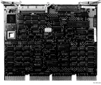
The KN210 CPU module set consists of the KN210 processor module, shown in Figure 1-1, and the KN210 110 module, shown in Figure 1-2. Both are quad-height modules for the Q22-bus (extended LSI-II bus). The KN210 processor module features the R3000 RISC processor. The KN210 110 module features built-in DSSI and -Ethernet controllers. The KN210 CPU module set is designed for use in high speed multiuser, multitasking environments.
The KN210 CPU module set is used in the DECsystem 5400. The DECsystem 5400 utilizes a BA213 enclosure. Refer to the BA213 Enclosure Maintenance for a detailed description of the enclosure.
The KN210 CPU module set and MS650 memory modules combine to form a RISC CPU/memory subsystem that uses the Q22-bus, DSSI bus, and Ethernet to communicate with mass storage and 110 devices. The KN210 CPU module set and MS650 modules mount in standard Q22-bus backplane slots that implement the Q22-bus in the AB rows and the CD interconnect in the CD rows. The KN210 CPU module set can support up
to four MS650 modules, if enough Q221CD slots are available.
The KN210 CPU module set communicates with the console device through the H3602-SA CPU cover panel, which also contains configuration switches, an LED display, and Ethernet connector.
Overview 1-3
Figure 1-2 KN210 I/O Module
ETHERNET DSSI
EJ
[image:27.510.65.376.101.421.2]J2 CD FINGERS
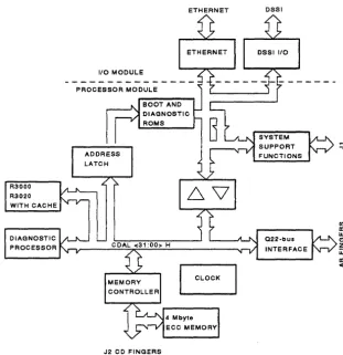
Figure 1-3 KN210 Block Diagram
1.2 R3000 RiSe
Processor
rn a:: w
"
~
LL
m <
MA-XOS10-89
The central processor of the KN210 module set is the R3000 RISe
Overview 1-5
The combined CPU/CPO processors provide the following features:
• 32-bit operation
• A 5-stage pipeline
• On chip cache control
• On chip memory management
• Coprocessor interface
1.3 Floating-Point Accelerator
The floating-point accelerator is implemented by the R3010 floating-point accelerator (FPA) chip. The R3010 FPA operates as a coprocessor for the R3000 processor and extends the R3000's instruction set to perform arithmetic operations on values in floating-point representations. The R3010 FPA interfaces with the R3000 processor to form a tightly-coupled unit with seamless integration of floating-point and fixed-point instruction sets.
1.4 Cache Memory
To maximize CPU performance, the KN210 module utilizes a system of cache memory. The cache memory is organized as two separate 64 Kbyte cache; one for instructions and the other for data.
1.5 Memory Controller
The main memory controller is implemented by a VLSI chip called the CMCTL. The CMCTL supports up to 64 Mbytes of ECC memory with a 500-550 ns cycle time for word transfers. This memory resides on up to four MS650 memory modules.
1.6 Diagnostic Processor
The diagnostic processor provides extensive diagnostic capabilities for the KN210 CPU module set.
1.7 MS650-BA Memory Modules
1.8 MS650-AA Memory Modules
The MS650-AA memory modules are 8 Mbyte, 450 ns, 39-bit wide arrays (32-bit data and 7-bit ECC) implemented with 256 Kbyte dynamic RAMs in zig-zag in-line packages (ZIPs). MS650-AA memory modules are single, quad-height, Q22-bus modules, as shown in Figure 1-4.
The MS650 modules communicate with the KN210 through the MS650 memory interconnect, which utilizes the CD rows of backplane slots 2 through 4, and a 50-pin ribbon cable. The KN210 memory subsystem supports a maximum of four memory modules.
MS650AA MS650BA
Figure 1-4 MS650 Memory Modules
1 .9
DSSI Interface
Overview 1-7
1 .10 Ethernet Interface
The KN210 110 module features an on-board network interface that is implemented through the LANCE chip and four 32K x 8 static RAMs. When used in conjunction with the H3602-SA CPU cover panel, this interface allows the KN210 CPU module set to be connected to either a Thin Wire or standard Ethernet network.
The Ethernet interface includes registers for control and status reporting as well as a DMA controller, a 24 word transmit silo and a 24 word receive silo.
1.11 Q22-bus Interface
The Q22-bus interface is implemented by the CQBIC chip, located on the KN210 processor module. The CQBIC chip supports up to 16-word, block mode transfers between a Q22-bus DMA device and main memory, and up to 2-word, block mode transfers between the CPU and Q22-bus devices. The Q22-bus interface contains the following:
• A 16-entry map cache for the 8,192-entry, main memory-resident "scatter-gather" map, used for translating 22-bit Q22-bus addresses into 26-bit main memory addresses
• Interrupt arbitration logic that recognizes Q22-bus interrupt requests BR7-BR4
• Q22-bus termination (240 [})
1.12 System Support Functions
System support functions are implemented by the system support chip (SSC), located on the KN210 processor module. The SSC provides console and boot code support functions, operating system support functions, timers, and many extra features, including the following:
• Word-wide ROM unpacking
• 1 Kbyte battery backed-up RAM
• Halt arbitration logic
• Console serial line
• Interval timer with 10 ms interrupts
• Time-of-year clock with support for battery back-up
• Programmable CDAL bus timeout counter
• Two programmable timers similar in function to the VAX standard interval timer
• A register for controlling the diagnostic LEDs
1.13 Firmware
The firmware consists of 256 Kbytes of 16 bit-wide ROM, located on two 128K EPROMs (one for each processor). The firmware gains control when the processor halts, and contains programs that provide the following services:
• Board initialization
• Power-up self-testing of the KN210 processor and I/O modules, and the MS650 modules
• Emulation of a subset of the VAX standard console (automatidmanual bootstrap, automatirlmanual restart, and a simple command language for examining/altering the state of the processor)
• Booting from supported Q22-bus devices, DSSI, or Ethernet
• Multilingual capability
• MOP support
1.14 Clock Functions
The clock chip provides the following functions:
• Generates two MOS clocks for the CPU and the main memory controller
• Generates three auxiliary clocks for other miscellaneous TTL logic
• Synchronizes reset signal for the CPU and the main memory controller
2
Installation and Configuration
2.1 Introduction
This chapter contains infonnation required to install the KN210 CPU module set in a system. The following topics are discussed:
• Installing the KN210 CPU module set
• Configuring the KN210
• KN210 connectors
• H3602-SA CPU cover panel
2.2 Installing the KN210 CPU Module Set
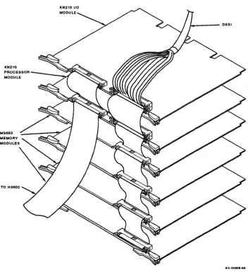
The KN210 CPU module set can only be installed in BA213 backplanes.
The KN210 I/O and processor modules must be installed in slots 1 and 2, respectively, of the Q221CD backplane (Figure 2-1). MS650 memory modules must be installed in slots immediately adjacent to the KN210 processor module. Up to four MS650 modules may be installed, occupying slots 3, 4, 5 and 6 respectively. A 50-pin ribbon cable is used to connect the KN210 processor and liD modules to each other. Another 50-pin cable is used to connect the KN210 processor module to the MS650 memory module(s), as shown in Figure 2-2.
A B
SLOT 1 SLOT 2
Q22-bus SLOT 3
SLOT 4 SLOT 5 SLOT 6 SLOT 7 SLOT 8 SLOT 9 SLOT 10 SLOT 11 SLOT 12
c
DC D INTERCONNECT
KN210 1/0 MODULE
KN210 PROCESSOR MODULE MS650 NO.1
MS650 NO.2 MS650 NO.3 MS650 NO.4
MA-X0608-8Q
KN210
MS650 MEMORY MODULES
[image:34.507.105.457.104.492.2]TO H3602
Figure 2-2 Cable Connections
2.3 Configuring the KN21 0
Installation and Configuration 2-3
IIA-xoeoa-II
The following parameters must be configured on the KN210:
• Operation switch
• Console serial line baud rate
• DSSI node ID
• Ethernet port connector selection
These parameters are configured using the H3602-SA CPU cover panel.
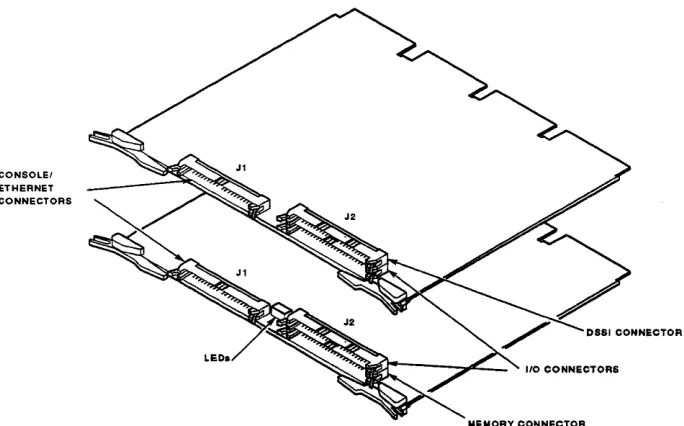
2.4 KN210 Connectors
The KN210 uses several connectors, and four rows of module fingers (A, B, C, and D) to communicate with the console device, main memory, the Q22-bus, the DSSI controller, and the Ethernet controller. The contact finger identification of the KN210 CPU and 1/0 modules is described in Appendix C.
The orientation of the connectors, and the LED indicators is shown in Figure 2-3.
[image:35.504.68.410.295.508.2]CONSOLEI ETHERNET CONNECTORS
Installation and Configuration 2-5
2.4.1 Console/Ethernet Connector
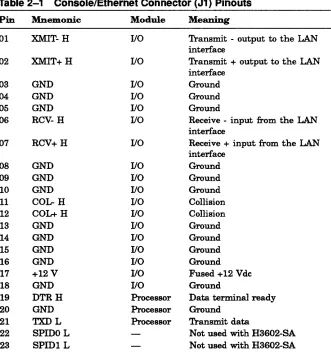
The ConsolelEthernet connector (J1) is a 40-pin connector used to bus signals to/from the Ethernet interface and system console, and for configuration and display purposes. A multi-tapped 40-pin cable provides the physical connection between the KN210 processor and 110 boards and the H3602-SA CPU cover panel. Table 2-1 gives the pinouts for the console connector.
Table 2-1 Console/Ethernet Connector (J1) Pinouts
Pin Mnemonic Module Meaning
01 XMIT- H I/O Transmit - output to the LAN interface
02 XMIT+H I/O Transmit + output to the LAN interface
03 GND I/O Ground
04 GND I/O Ground
05 GND I/O Ground
06 RCV-H I/O Receive - input from the LAN
interface
07 RCV+H I/O Receive + input from the LAN
interface
08 GND I/O Ground
09 GND I/O Ground
10 GND I/O Ground
11 COL- H I/O Collision
12 COL+H I/O Collision
13 GND I/O Ground
14 GND I/O Ground
15 GND I/O Ground
16 GND I/O Ground
17 +12V I/O Fused +12 V dc
18 GND I/O Ground
19 DTRH Processor Data terminal ready
20 GND Processor Ground
21 TXDL Processor Transmit data
22 SPIDO L Not used with H3602-SA
[image:36.504.99.430.217.576.2]Table 2-1 (Cont.) Console/Ethernet Connector (J1) Pinouts
Pin Mnemonic
24 RXDL
25 RXDH
26 SPIDO L
27 +5V
28 CONBITRATE2 L 29 CONBITRATE1 L 30 CONBITRATEO L
31 LEDCODEOL
32 LEDCODE1L
33 LEDCODE2 L
34 LEDCODE3L
35 ENBHALTL
Module Processor Processor Processor Processor Processor Processor Processor Processor Processor Meaning Receive data Receive data
Not used with H3602-SA Fused +5 Vdc
Console bit rate <02:00>. These three bits determine the console baud rate. They are configured using the select switch on the inside of the H3602-SA. LED code register bits <03:00>. When asserted each of these four output signals
Lights a corresponding LED on the module.
LEDCODE<03:00> are asserted (low) by power-up and by the negation of DC OK when the processor is halted. They are updated by boot and diagnostic programs from the BDR.
Halt enable. This input signal controls the response to an external halt condition. If ENBHALT is asserted (low), then the KN210 halts and enters the console program if any of the following occur:
• The program executes a halt instruction in kernel mode.
• The console detects a break character.
Installation and Configuration 2-7
Table 2-1 (Cont.) Console/Ethernet Connector (J1) Pinouts
Pin Mnemonic
86
87
8S
89
40
BDCODEIL BDCODEOL
VBATH
CPUCODEIL CPUCODEOL
Module
Processor
Processor
Processor Processor
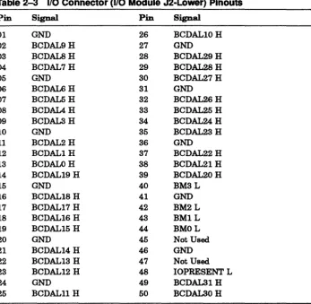
2.4.2 OSSI/I/O Connector
Meaning
If ENBHALT is negated (high), then the halt line and break character are ignored and the ROM program responds to a halt instruction by restarting or rebooting the system. ENBHALT is read by software from the BDR.
Boot and diagnostic code <01:00>. This 2-bit code indicates power-up mode, and is read by software from the BDR.
Battery backup voltage for the TODR clock.
CPU code <01 :00>. This 2-bit code is read by software from the BDR. The configuration for the CPU code is as follows:
00 Normal operation 01 Reserved
10 Reserved 11 Reserved
Table 2-3 lists the pinouts for the I/O interconnect portion of J2 (lower 50 pins). Table 2-2 lists the pinouts for the DSSI portion of J2 (upper 50 pins).
Table 2-2 DSSI Connector (1/0 Module J2-Upper) Pinouts
Pin Mnemonic Pin Mnemonic
51 DSSIDATAO L 76 VTERMH
52 GND 77 VTERMH
53 DSSIDATA1 L 78 VTERMH
54 GND 79 GND
55 DSSIDATA2 L 80 Unused
56 GND 81 GND
57 DSSIDATA3 L 82 Unused
58 GND 83 GND
59 DSSIDATA4 L 84 Unused
60 GND 85 GND
61 DSSIDATA5 L 86 DSSIBSYL
62 GND 87 GND
63 DSSIDATA6 L 88 DSSIACKL
64 GND 89 GND
65 DSSIDATA7 L 90 DSSIRSTL
66 GND 91 GND
67 DSSIPARITY L 92 Unused
68 GND 93 GND
69 Unused 94 DSSISELL
70 GND 95 GND
71 Unused 96 DSSICID L
72 GND 97 GND
73 VTERMH 98 DSSIREQ L
74 VTERMH 99 GND
Installation and Configuration 2-9
Table 2-3 1/0 Connector (1/0 Module J2-Lower) Pinouts
Pin SigDal Pin SigDal
01 GND 26 BCDALI0H
02 BCDAL9H 27 GND
03 BCDALBH 28 BCDAL29H
04 BCDAL7H 29 BCDAL28H
05 GND 30 BCDAL27H
06 BCDAL6H 31 GND
07 BCDAL5H 32 BCDAL26H
08 BCDAIAH 33 BCDAL25 H
09 BCDALSH 34 BCDAL24H
10 GND 35 BCDAL23H
11 BCDAL2H 36 GND
12 BCDALIH 37 BCDAL22 H
13 BCDALOH 38 BCDAL21 H
14 BCDAL19 H 39 BCDAL20H
15 GND 40 BM3L
16 BCDAL18 H 41 GND
17 BCDAL17 H 42 BM2L
18 BCDAL16 H 43 BMIL
19 BCDAL15 H 44 BMOL
20 GND 45 Not Used
21 BCDAL14 H 46 GND
22 BCDAL13 H 47 Not Used
23 BCDAL12 H 48 IOPRESENT L
24 GND 49 BCDALSl H
25 BCDALll H 50 BCDALSOH
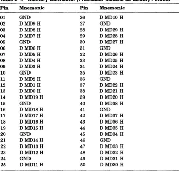
2.4.3 Memory Connector
Table 2-4 lists the pinouts for the memory portion of J2 Oower 50 pins). Table 2-3 lists the pinouts for the I/O interconnect portion of J2 (upper 50 pins).
Table 2-4 Memory Connector (Processor Module J2-Lower) Pinouts
Pin Mnemonic Pin Mnemonic
01 GND 26 D MDI0 H
02 DMD9H 27 GND
03 DMD8H 28 D MD29 H
04 DMD7H 29 D MD28H
05 GND 30 DMD27 H
06 DMD6H 31 GND
07 DMD5H 32 D MD26 H
08 DMD4H 33 D MD25 H
09 DMD3H 34 D MD24 H
10 GND 35 D MD23 H
11 DMD2H 36 GND
12 DMDIH 37 D MD22 H
13 DMDOH 38 D MD21 H
14 DMD19H 39 D MD20 H
15 GND 40 D MD38 H
16 DMD18H 41 GND
17 DMD17H 42 D MD37 H
18 DMD16H 43 D MD36H
19 DMD15 H 44 D MD35 H
20 GND 45 DMD34H
21 DMD14H 46 GND
22 DMD13H 47 D MD33 H
23 DMD12H 48 D MD32 H
24 GND 49 D MD31 H
[image:41.507.61.413.143.478.2]Installation and Configuration 2-11
2.5 H3602-SA CPU Cover Panel
The H3602-SA CPU cover panel is a special 110 panel that is used in BA213 enclosures. A multi-tapped 40-pin ribbon cable provides the physical connection between the H3602-SA CPU cover panel and the Jl connectors of both the KN210 processor and 110 modules. The H3602-SA fits over backplane slots 1 and 2, covering both the KN210 110 and processor modules.
The H3602-SA CPU cover panel (Figure 2-4) includes the features and controls specified in Table 2-5.
Table 2-5 H3602·SA Features and Controls
Outside Inside
Modified modular jack (MMJ) Baud rate rotary switch SLU connector
Operation switch Battery backup unit (BBU) for TODR clock Hexadecimal LED display 40-pin cable connector
Function switch List of baud rate switch settings Standardll'hin Wire Ethernet
connectors
Standardll'hin Wu-e Ethernet selector
II
~:
~MA·X0787·88
3
Architecture
This chapter describes KN210 registers, instruction set, and memory. The chapter covers the following KN210 topics:
•
RISC processor•
Floating-point accelerator•
Cache memory•
Main memory system•
Console serial line•
Time-of-year clock and timers•
Boot and diagnostic facility•
Q22-bus interface•
Mass-storage interface•
Network interface3.1 R3000 RiSe
Processor
The central processor of the KN210 is the R3000 RISe processor plus its associated R3010 floating-point unit.
3.1.1 Processor Features
The R3000 chip implements two tightly coupled processors in a single VLSI chip. One processor being a 32-bit CPU, and the second being a system control processor (CPO).
The combined CPU/CPO processors provide these features.
• 32-bit operation - The R3000 is a 32-bit machine with 32 32-bit registers,all addressing is 32-bits.
• Pipelined - The CPU contains a five stage pipeline capable of executing one instruction per 50 ns cycle.
• On chip cache control - The R3000 supports separate instruction and data caches of up to 256 Kbytes. (The KN210 supports 64 Kbytes each.) Both caches can be accessed in a single CPU cycle.
• On chip memory managment - A four Gbyte virtual address space is mapped with a 64 entry fully associative translation lookaside buffer.
• Coprocessor interface - The R3000 provides a tightly coupled coprocessor interface for up to four coprocessors. The first CPO is contained on the CPU chip and the second CPl is the floating-point unit. CP2 and CP3 are unused in the KN210.
• Write buffers - The KN210 uses four R3020 4-word deep write buffers. All writes pass through these write buffers.
NOTE
Because all writes pass through the write buffers, software writing to 110 devices must wait for the write buffers to empty before reading from locations that could be affected by these 110 writes. This can be accomplished by conditionally branching on the coprocessor 3 condition. (DC3F branches if the WB is not empty and BC3T·branches if the WB is empty.)
3.1.1.1 General Purpose Registers
Architecture 3-3
3.1.1.2 Instruction Set
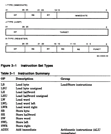
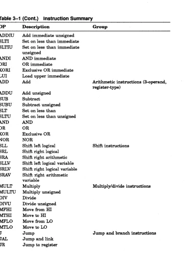
R3000 instructions have three types, as shown in Figure 3-1. A summary of R3000 instructions is given in Table 3-1.
I-TYPE (IMMEDIATE)
31 26 25 21 20
OP RS RT
J-TYPE (JUMP)
31 26 25
OP
R-TYPE (REGISTER)
31 26 25 21 20
[image:46.504.91.446.144.571.2]OP RS RT
Figure 3-1 Instruction Set Types
Table 3-1 Instruction Summary OP LB LBU LH LHU LW LWL LWR
SB
SH SW SWL SWR ADDI Description Load byteLoad byte unsigned Load halfword
Load halfword unsigned Load word
Load word left Load word right Store byte Store halfword Store word Store left Store right Add immediate
1615 0
IMMEDIATE
0
TARGET
16 15 11 10 6 5 0
RD RE FUNCT
MA-X0620-811
Group
Load/Store instructions
Arithmetic instructions (ALU
Table 3-1 (Cont.) Instruction Summary
OP Description Group
ADDIU SLTI SLTIU ANDI ORI XORI LUI ADD ADDU SUB SUBU SLT SLTU AND OR XOR NOR SLL SRL SRA SLLV SRLV SRAV MULT MULTU DIV DIVU MFHI MTHI MFLO MTLO J JAL JR
Add immediate unsigned Set on less than immediate Set on less than immediate unsigned
AND immediate OR immediate
Exclusive OR immediate Load upper immediate Add
Add unsigned Subtract
Subtract unsigned Set on less than
Set on less than unsigned AND
OR
Exclusive OR NOR
Shift left logical Shift right logical Shift right arithmetic Shift left logical variable Shift right logical variable Shi'ft right arithmetic variable
Multiply
Multiply unsigned Divide
Divide unsigned Move from HI Move to HI Move from LO Move to LO Jump
Jump and link Jump to register
Arithmetic instructions (3-operand, register-type)
Shift instructions
Multiply/divide instructions
[image:47.504.62.450.60.599.2]Architecture 3-5
Table 3-1 (Cont.) Instruction Summary
OP Description Group
JALR BEQ BNE BLEZ BGTZ BLTZ BGEZ BLTZAL
Jump and link. register Branch on equal Branch not equal
Branch on less than or equal to zero
Branch on greater than zero Branch on less than zero Branch on greater than or equal to zero
Branch on less than zero and link.
BGEZAL Branch on greater than or equal to zero and link. SYSCALL System call
BREAK Break LWCz SWCz MTCz MFCz CTCZ CFCz COPz BCzT BCzF MTCO MFCO TLBR
TLBWI
TLBWR TLBP RFELoad word from coprocessor Store word to coprocessor Move to coprocessor Move from coprocessor Move control to coprocessor Move control from
coprocessor
Coprocessor operation Branch on coprocessor z true Branch on coprocessor z false Move to CPO
Move from CPO
Read indexed TLB entry Write indexed TLB entry Write random TLB entry Probe TLB for matching entry
Restore from exception
Special instructions
Coprocessor instructions
System control coprocessor (CPO)
3.1.2 Coprocessors
The R3000 can operate with up to four tightly coupled coprocessors, two of which are implemented in the KN210.
3.1.2.1 Coprocessor (0)
The system control coprocessor (CPO) is part of the R3000 chip itself. Its function is to support the virtual memory system and exception handling functions. It contains the translation lookaside buffer (TLB) plus the following registers:
• EntryHi· High half of a TLB entry.
• EntryLo • Low half of a TLB entry.
• Index· Programmable pointer into the TLB.
• Random· Pseudo-random pointer into the TLB.
• Status -Mode, interrupt enables, and diagnostic status information.
• Cause· Cause of last exception.
• EPC· Exception program counter.
• Context· Pointer into kernel's virtual page table entry array.
• BadVA· Most recent bad virtual address.
• PRId • Processor revision identification.
3.1.2.2 Coprocessor (1)
Coprocessor one (CP1) is the R3010 floating-point unit. The R3010 floating-point processor implements the IEEE arithmetic functions.
3.1.3 Memory Management
1024Mbyte
(
r
512Mbytet
612Mbyta!
r
[image:50.508.103.454.100.391.2]I
)
2048Mbyte)
I
~ Figure 3-2R3000 VIRTUAL
KSEG 2 KERNEL MAPPED
COOOOOOO KSEG 1 KERNEL UNMAPPED UNCACHED
AOOooOOO KSEG 0 KERNEL UNMAPPED CACHED 80000000 KUSEG USER MAPPED CACHEABLE 00000000
j.
1
1
NYWHERE YWHERE ... \.R3000 PHYSCIAL
UNUSED 20000000 110 10000000 MEMORY 00000000
Architecture 3-7
j
258Mby t4Mbyt. { 268Mbyte{ 258Mb te{
258Mbyt. {
j ... ,,, ...
M.,,"!
DIAGNOSTIC PRoceSSOR PHYSICAL
NO ACCESS
30400000 Q22·bus 30000000 DIAGNOSTIC PROCESSOR 110 SPACE 20000000 DIAGNOSTIC PROCESSOR MEMORY SPACE 00000000 UA·XO.17 •••
2000 0000
1 FC2 0000
1 FCO 0000
1800 0000 1700 0000
1600 0000
1500 0000
1400 0000
1000 0000
40 0000
o
R3000 PHYSCIAL
NO ACCESS ROM WEAR VRR Q22-bus MEMORY
64 Mbyte
l
-Figure 3-3 R3000 to 110 Memory Map
{
r!
{--H
I \."""-CP BUS
-
---
...NO ACCESS
Q22-bus MEMORY
NO ACCESS
NO ACCESS
NO ACCESS
ROM DUAL ACCESS
--30 40 0000
30 2F
2F
28 00 0000 C2 0000
CO 0000
00 0000
26 00 0000
00 0000 25
24
20
20 20
00 0000
04 0000
00 2000 00 0000
40 0000
MEMORY 64 Mbyte
_ _ _ _ _ _ _ --'0
[image:51.508.70.417.126.507.2]Architecture 3-9
3.1.3.1 Operating Modes
The R3000 has two operating modes, kernel and user. All exceptions are handled in kernel mode. User mode is entered through the restore from exception (RFE) instruction.
User mode - 2 Gbytes of virtual address are available in this mode. Virtual addresses are extended with a 6-bit process identifier field allowing up to 64 user processes. All references in this mode are mapped through the TLB. Pages can be made cacheable or uncacheable through the use of hits within the TLB entries.
Kernel mode - contains four separate segments.
• KUSEG - references treated the same as user mode.
• KSEGO - references cached but not mapped.
• KSEG 1 - references not cached and not mapped.
• KSEG2 - references mapped and cacheability determined through the TLB entries.
3.1.3.2 EntryHi and EntryLo Registers
These registers are used to read, write, or probe the TLB. During exceptions, these registers are loaded with information about the address that caused the exception. The format of these registers is the same as the format of a TLB entry. A TLB EntryHi register (EH) is shown in Figure 3-4. A TLB EntryLo register (EL) is shown in Figure 3-5.
63 4443 3837 32
VPN PIO ZEROS
MA-X0621-8e
Data Bit Definition
EntryHi<63:44> (VPN) Virtual page number. Contains bits <31:12> of the virtual address.
EntryHi<43:38> (PID) Process ID field. Allows multiple processes to share the TLB.
EntryHi<37:32> EntryHi<5:0> Unused. Read as O's.
31 12 11 10 9 8 7
PFN ZEROS
o
[image:53.504.38.413.81.482.2]MA-X0622-89
Figure 3-5 TLB EntryLo Register
Data Bit Definition
EntryLo<31:12> (PFN) Page frame number. Contains bits <31:12> of the physical address.
EntryLo<11>
EntryLo<10>
EntryLo<8>
EntryLo<7 :0>
(N) Non-Cacheable. When set, the page mapped by this entry will not be cached.
(D) Dirty. Setting this bit marks the page mapped by this entry as writeable.
(V) Valid. This bit marks the page as valid, letting translation take place, otherwise a TLBL or TLBS miss will occur.
(G) Global. When set, the RaOOO will ignore the PID match requirement for translations through this entry.
Architecture 3-11
3.1.3.3 Index Register
The index register (IR) is used to index into the TLB when doing either TLB reads or TLB writes. The high-order bit returns status information for the probe instruction. The format for the index register is shown in Figure 3-6.
31 30 14 13 8 7
ZEROS INDEX ZEROS
o
MA-X0623-8a
Figure 3-6 Index Register
Data Bit Definition
Index<31> (P) Probe failure. Set to (1) if the last probe instruction failed. lndex<30:14> Unused. Read as O's.
Index<13:8> Indexes the TLB entry for TLB reads or writes. Index<7:0> Unused. Read as O's.
3.1.3.4 Random Register
The random register (RR) is used when replacing TLB entries. The TLBWR instruction is used to write the TLB entry pointed to by this register. The first 8 TLB entries will never be written using the TLBWR instruction. The format for the random register is shown in Figure 3-7.
31 1413 8 7
ZEROS RANDOM ZEROS
o
MA-X0624-88
Data Bit Definition
Random<31:14> Unused. Read as D's.
Random<13:8> Random index into the TLB ranging from 8 to 63. Random<7:0> Unused. Read as D's.
3.1.4 Exception Handling Registers
Exceptions are handled through the use of six coprocessor zero (CPO) registers and one module specific interrupt status register. Software uses these registers during exception handling to determine the cause of the exception. These registers are described in the following sections.
3.1.4.1 Cause Register
The cause register (CR) is a 32-bit register used when servicing exceptions. It describes why the last exception was taken. All bits in this register are read only except for the SW bit. The format for the cause register is shown in Figure 3-8.
SO
ZERO
3130 2928 27
[image:55.505.56.415.320.571.2]ZEROS
Figure 3-8 Cause Register
Data Bit Definition
16 15 10 9 8 7 6 5 2 1 0
ZEROS - - - '
MA-X0656-8V
CR<31> (BD) Branch delay. Set to 1 if last exception was taken while executing in a branch delay slot.
CR<30> Unused. Read as zero.
CR<29:28> CE<1:0> Coprocessor error. Indicates the unit number referenced when a coprocessor unusable exception is taken.
Data Bit
CR<15:10>
CR<7:6> CR<5:2>
CR<1:0>
Architecture 3-13
Definition
IP<5:0> Interrupt pending. Indicates which of the external interrupts are pending. Table 3-2 shows the mapping of physical interrupt requests to the cause register IP<5:0> status bits. Figure 3-9 shows the flow of the interrupt acknowledge daisy chain.
SW <1:0> Software interrupts. Indicates which software interrupts are pending. These bits are read/write. Unused. Read as O's.
(EC) Exception code. The exception code field is described in the following table.
Number Name Description
0(10) INT External interrupt
1 MOD TLB modification exception 2 TLBL TLB miss exception Ooad or fetch) 3 TLBS TLB miss exception (store)
4 ADEL Address error exception (load or fetch) 5 ADES Address error exception (store) 6 IBE Bus error exception (fetch)
7 DBE Bus error exception Ooad or fetch)
8 SYS Syscall exception
9 BP Breakpoint exception
10 RI Reserved instruction exception 11 CPU Coprocessor unusable exception 12 OVF Arithmetic overflow exception 13-15 Reserved
Table 3-2 R3000 Interrupt Mapping
Vector Bit Priority Interrupt Request Register
IP<5> 2 FPU IP<4> 1 HALT
IP<3> 3 PWRFL, MER1, MERO, WEAR
IP<2> 4 100 Hz ->BIRQ7 VRR3 IP<l> 5 nSSI ->NI ->BIRQ6 VRR2 IP<O> 6 BIRQ5 ->Console ->Timers VRR1
->BIRQ4
PROCESSOR MODULE
R3000
VRRO
100 Hz CLOCK
NO 110 ~ MODULE / '
-I
Q22·bu.
Figure 3-9 Interrupt Acknowledge Daisy Chain
Corresponding Diagnostic Processor IPL
IPL17 IPL16 IPL15 IPL14
110 MODULE
[image:57.507.57.413.95.430.2]Architecture 3-15
3.1.4.2 Exception Program Counter
The exception program counter (EPC) contains the virtual address of the instruction which caused the exception to be taken. If the instruction is in a branch delay slot, the EPC will contain the virtual address of the preceding branch or jump instruction.
3.1.4.3 Status Register
The status register (SR) is a 32-bit register containing various processor status. The format for the status register is shown in Figure 3-10.
31 29 27 23 22 21 20 1 9 18 17 16 15 8 7 6 5 4 3 2 o
MA-X062&-18
Figure 3-10 Status Register
Data Bit Definition
SR<31:28> CU<3:0> Coprocessor usability. CU<3:0> controls the availability of the four possible coprocessors. Setting a CU bit to 1 enables the coprocessor.
SR<27:23> Unused_ Read as O's.
SR<22> (BEV) Bootstrap exception vector. When set to 1 causes the R3000 to use the alternate bootstrap vectors for UTLB miss and general exceptions.
SR<21> (TS) Translation buffer shutdown. Set to 1 if the RaOOO has disabled the translation buffer due to error.
SR<20> (FE) Parity error. Set to 1 if a cache parity error occurs. Cleared by writing a 1.
SR<19> (CM) Cache miss. Set to 1 if most recent D-cache load resulted in a miss when the D-cache is isolated.
SR<18> (PZ) Parity zero. Setting to 1 forces parity bits to
o.
Data Bit
SR<15:10>
SR<7:6> SR<5> SR<4> SR<3> SR<2>
Definition
(lSC) Isolate cache. Isolates the D-cache from the memory system.
INTR<7 :2> Interrupt mask. Setting these INTR bits to 1 enables their corresponding hardware interrupt.
INTR<1:0> Interrupt mask. Setting these INTR bits to 1 enables their corresponding software interrupt.
Unused. Read as O's.
(KUO) Kernel/user mode, old. Set to 0 if kernel, 1 if user. (lEO) Interrupt enable, old. Set to 1 to enable, 0 to disable. (KUP) Kernel/user mode, previous. Set to 0 if kernel, 1 if user. (IEP) Interrupt enable, previous. Set to 1 to enable, 0 to disable.
(KUC) Kernel/user mode, current. Set to 0 if kernel, 1 if user. (IEC) Interrupt enable, current. Set to 1 to enable, 0 to disable.
3.1.4.4 BadVaddr Register
The BadVaddr register (BVA) saves the virtual address for any addressing exception.
3.1.4.5 Context Register
The context register (CR) is used by the UTLB miss handler. The CR saves some of the same information as the BadVaddr register. The format for the context register is shown in Figure 3-11.
31 21 20 2 1 0
PTEBase BadVPN
[image:59.505.55.411.89.336.2]MA-X0627-80
Architecture 3-17
Data Bit
CR<31:21>
CR<20:2>
Definition
(PTEBase) Page table entry base. Holds the base for the page table entry.
(BadVPN) Bad virtual page number. Holds the failing virtual page number. Read only. Set by hardware.
Unused. Read as O's.
3.1.4.6 Processor Revision Identifier Register
The processor revision identifier register (PRR) contains implementation and revision numbers for the RaOOO chip. The format for the processor revision identification register is shown in Figure 3-12.
31 16 15 8 7
PTEBase IMP REV
o
MA-X0652-811
Figure 3-12 Processor Revision Identifier Register
Data Bit Definition
PRR<31:16> Unused. Read as O's.
PRR<15:8> IMP<7:0> Implementation identifier. PRR<7:0> REV<7:0> Revision identifier.
3.1.4.7 Interrupt Status Register
The interrupt status register, (RaOOO address 1008 4000; diagnostic processor address 2008 4000) returns information concerning the four conditions which can cause an INTRa interrupt. It can be accessed by either processor but only has meaning for the RaOOO. The diagnostic processor must make sure ISR<2:0> are 0 before transferring control