~'----~_=
cQ].--::0~~o
~=--o
(f@X1D_O[2)=-o _ _ )po box 6528 denver, colorado 80206 (303)
n7-7133
TABLE OF CONTENTS
I. INTRODUCTIO'N ... 1
II. SET UP AND OPERATION ... 1
A. Free Standing Display ... 3
B. Light Pen and Display Control ... 4
C. External Sync and Video Mixing ... 6
III. THEORY OF OPERATION ... 8
IV. SPECiFiCATIONS ... 10
V. CONSTRUCTION ... 11
VI. TROUBLESHOOTING ... 14
VII. APPENDIX ... 16
A. Block Diagram ... . . . .. 17
B. Timing Diagrams ... 18
C. Sample Software Routines ... 21
D. Parts List ... . . . • . . . .. 42
1. Graphics Board ... " ... 42
2. Light Pen ... 43
E. Digital Group Bus Pin Assignments ... 44
1. Memory Bus. . . .. 44
2. 1/0 Bus ... ; ... 45
3. TVC Pin Out ... 46
4. Back Panel Connector Pin Out ... 47
F. Cabling ...•. 48
G. Parts Layout ... 51
1. Graphics Board ... 51
2. Light Pen ... 52
3. Paddle Card. . . .. 53
H. Schematic ... 54
1. Graphics Board ... 54
ADDENDUM TO GRAPHICS-256 DOCUMENTATION
1.
Included with your Graphics Display Board kit are two 220 pfd
capacitors. Attach one between IC33 pin 1 and ground and the other
between IC39 pin 1 and ground.
2.
In the Vertical Output Circuitry of the schematic, change the label U42
of the 7420 with pins 1,2,4,5 and 8 to U27.
I.
INTRODUCTION
The Digital Group High Resolution Graphics Display board is a high resolution graphics interface with 256 display points on each of 256 raster scan lines. Sufficient graphics power is available to plot detailed charts and graphs, draw pictures or sketches, create intricate game boards, or run space-war simulations. The possibilties are limited only by your imagination. Utilizing a memory mapping technique, the High Resolution Graphics Display does not use up RAM already dedicated tothe CPU since it contains its own 8K bytes of onboard memory. This on board memory is seen by the CPU as another 8K RAM board and can be used for additional program memory when graphics operation is not desired. A separate board anable/disable line is available to selectively enable the board under software control. allowing overfapping of other memory. Only CPU access is disabled, therefore display is continuous. This effectively gives you 72K of available memory. The Light Pen functions with the High Resolution Graphics Display under software control to allow the user tb precisely indicate points on the screen. Not only does the Light Pen allow you to indicate a character or line on the display, but it gives you the ability to draw detailed pictures by precisely knowing its position on the screen.
A video mixer circuit and external sync lines are provided in order to synchronize the display with your TV readout board. Either the TV readout or graphics may be selected manually or under software control, or they may be superimposed for writing captions on charts and graphs, messages on game displays, or monitoring the operation of your program. Thevideo output is compatible with a TV monitor.
II. SET UP AND OPERATION
GeneralThe Digital Group High Resolution Display has three basic modes of operation including Free Standing Display, Light Pen and Graphics Control, and External Sync and Video Mixing. Following is a discussion of each mode and a description of setting up the Graphics Display for each mode in a Digital Group System.
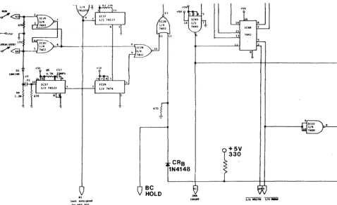
In addition to the set up of the Graphics Display, some modifications to the Z80 CPU board and motherboard must be made. First. install a germanium diode (1 N60 or 1 N48) between the 2.2k pull up resistor and ROM enable line to IC20 pin 14 on the Z80 CPU board. This requires cutting the trace between IC20 and the pull-up. This is diode A in Figure 1. Second, install a 1 N4148 diode (diode B) and a 330 ohm, V4watt resistor according to Figure 2. Cut the trace to IC28 pin 12 between the 470 ohm pull down resistor and pin 6 of IC 21. For some early disk installations, IC21 has been removed from the CPU. If IC21 has been removed, do not install the 330 ohm resistor. Third, connect a wire between pin 12 of IC28 and finger BC of the edge connector on the Z80 CPU board.
eRA 1N60
a.alt
l.21t
-1-HI (not aSSltp'led
to any pin
ec
HOLDCRe 1N4148
+SV
+5V
330
16
FIGURE 2. INSTALLATION OF CRB, 330 ohm resistor on Z80 CPU.
If your system has been configured for a Floppy Disk Controller, diode B may already be installed as well as a diode between BC on the edge connector and pin 12 of IC28. If so, removethe diode between BC and IC28 and install it on the disk controller board between pin 36 of the edge connector and pin 11 of IC34. Refer to Figure 3 forthe proper orientation of the diode on the disk controller. The trace to pin 36 must be cut.
Fourth, connect a wire between pin 20 of the memory bus and pin Be of the Z80 CPU slot or the bottom ofthe motherboard.
1N4148
36 11 12
[image:5.617.73.551.50.342.2] [image:5.617.61.539.501.711.2]A.
Free Standing Display
General
This mode of operation allows the user to perform all plotting and pictorial functions of the Graphics Display as well as use of the board as 8K of system memory. The board is inserted in a memory slot without connecting the associated cabling and Light Pen. Since the Graphics Control Cable, Graphics Input Cable and Light Pen are not connected, several functions are not available. Unavailable functions are: use of the Light Pen. superimposing an external video signal such as the TVC-64 output over the graphics display and software control of video and the ability to enable or disable the memory when overlapping another memory board in the system.
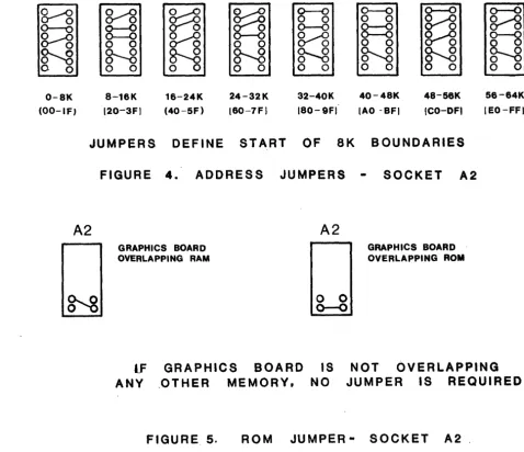
Set up for this mode requires installing several jumpers for addressing and memory accessing. Figure 4 shows the address jumper configurations for any 8k block of memory in a Digital Group Z80 based system. Refer to the Parts Layout in the Appendix to locate the jumper socket. Pins 7,8, and 9 of A2 are used for jumpering the ROM enable signal (ROM), which also disables RAM boards in the Digital Group system. Figure 5 shows the proper jumper configuration for ROM when the Graphics Display overlaps either a RAM board or a ROM board. If the Graphics Display is not overlapping other memory, the
RC5i\if
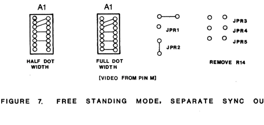
jumper may be omitted or jumpered as if it were overlapping a RAM board.Jumper socket A 1 and jumpers JPR1 through JPR5 set up the video section of the Graphics Display. The video output may be set up for either composite video (video with sync signals) or separate video and sync signals. Separate video and syncs would be used with the Digital Group Data Monitor without a sync separator (MON90-COMP). Most monitors will require composite video. For the Free Standing Mode. the video output will be connected at Pin M of the memory bus and JPR2 must be installed.
Two dot widths are available, half dot width and full dot width. Half dot width makes a more defined dot and is recommended for initial testing. Full dot width makes adjacent dots touch causing the display to appear brighter.
0-8X (OO-IF)
~
g---g
o
0N
o
0 a-16K 120-3F) 16-24K (40-5F)
~
g/g
0--0o
0
N
o
024-32K 160-7F)
0----0
o
00--0
~
N
o
032-40K 180-9FI
0--0
o
08=8
o
0N
o
040-48K lAO -BF)
~
N
o
048-56K tCO-DFt
56-64K IEO-FFI
JUMPERS
DEFINE
START
OF
8K
BOUNDARIES
[image:6.621.60.539.333.745.2]A2
FIGURE
4.
ADDRESS
JUMPERS
SOCKET
A2
GRAPHICS BOARD OVERLAPPING RAM
tF
ANY
GRAPHICS
BOARD
.OTHER
MEMORY.
A2
GRAPHICS BOARD OVERLAPPING ROM
o
0
0--0
IS
NO
NOT
OVERLAPPING
JUMPER
IS
REQUIRED
FIGURE
5.
ROM
JUMPER -
SOCKET
A2.
-3-COMPOSITE VIDEO OUT
Install the jumpers as pictured in Figure 6 with the desired dot width. Connect the video from pin M of the memory bus to the video input of the monitor.
A1
A1
~
~
~
0
0
JPR30
0
JPR1 JPR4
l.LPR2
0----0
JPR5HALF DOT FULL ,_DOT
WID.TH. WIDTH
[image:7.615.75.522.98.306.2] [image:7.615.83.514.388.593.2](VIDEO FROM PIN .. M)
FIGURE
6.
,FREE
STA·NDING
MODE.
COMPOSITE
VIDEO
OUT
SEPARATE VIDEO AND SYNC OUT
Install the jumpers as pictured in Figure 7 with the desired dot width. Remove R14 from the board. The horizontal sync (HORSYN) and vertical sync (VERSYN) are the bottom two pins of socket A3. Connect HORSYN to pin 6 of the edge connector of the Digital Group Data Monitor and VERSYN to pin 9. Connect the video out from pin M of the memory bus to pin 8 of the Data Monitor.
A1
A1
~ ~
0----0
0
0
JPR3
0
JPR1
0
0
JPR4b
0
0
JPR5 JPR2
HALF DOT FULL DOT REMOVE R14
WIDTH WIDTH
[VIDEO FROM PIN M]
FIGURE
7.
FREE
STANDING
MODE.
SEPARATE
SYNC
QUIT
B. Light Pen and Display Control
General
Operation of the Graphics Display with the Light Pen and Display Control requires installation ofthe Graphics Control Cable, Graphics Input Cable, Light Pen Cable with Paddlecard and the eight COflductor double ended Molex cable. Refer to Appendix E for Digital Group bus pin assignme:nts and Appendix F for cabling diagrams when installing the various cables. Input Cable Installation
Graphics Control Cable Installation
Insert the 16 pin dual in line connector into socket A4 and connect the two eight position Molex connectors to pins D through W of the back panel connector. Refer to App'endix F for the proper orientation of the cable and the back panel connector pin out.
Eight Conductor Cable Installation
Connect one end of the cable to pins 4 through 11 of the back panel connector and the other end to the Output Port you have assigned to the Graphics Display. Refer to Appendix E for the back panel connector pin out and the 1/0 bus pin out. Light Pen and Paddle Card Installation
The Light Pen Cable includes the paddle card for connection to the back panel. Light pen operation is independent of the video output mode and external video mode. The paddle card is plugged into the back panel connector with the side with pins 1 and 22 marked oriented up. Connect the video cable forthe monitor to VIDEO OUT and the shield to one of the GND holes. Ught Pen Operation and Control Signals
Control Signals
One eight bit output port is utilized for control sig nals to the Graphics Display. Seven of the bits control various functions of the display while one is used as feedback to the Light Pen to turn on the LED. Following is a brief description of each signal and its effect on the display.
lED,
MSB of output data, will turn on the LED in the Light Pen handle when at a logic (3. The LED may be used to signal the user that the pushbutton on the Light Pen is closed (pushed), to tell the user that the computer is busy and unable to input Light Pen data, or any other function the user chooses.A 16, MSB-1 of output data, is used to enable or disable the memory of the Graphics Display. When A 16 is at a logic 1, t~e
memory is enabled. If the Graphics Display memory is overlapping a RAM board, that RAM will bedisabled when A16 is high and the memory at that address is accessed. To access the RAM board instead of the Graphics Display, A 16 must be at 'a logic (3. The
Ro'M'
jumper must be installed as in Figure 5 for overlapping RAM.EXTVID. MSB-2, allows an external video signal to be superimposed overthe Graphics Display video. When EXTVID is high, the external video is displayed. When low, only the Graphics video is displayed. The external sync will still effectthe display however.
'i"Nv,
MSB-3, will invert the output video when at a logic (3. WheniN\7
is a logic 1 the video will be white on black. Do not invert the video with external video superimposed on the Graphics Display.GRAPH, LSB+3, is similar in function to EXTVID. A logic 1 on this bit enables the graphics data to be displayed in the output video. A logic (3 will display only the external video, provided EXTVID is high.
----
WHITE, LSB+2. will fill the scr.een with dots when at a low level. In the normal white on black video display this will result in an all white screen. WhenWH'iTE
is a (3 the CPU will see an FFH in al18K memory locations of the Graphics Display. Data may be written into memory whenW'HiTE'
is low but cannot be read. The data can be read when WRITE goes high. WRiTE mustbe high at all times if the Graphics Display is being utilized as system memory.WR'i'TE
in conjuction with PSEL(3 will generate a signal labeledB'i:'AC'K
which blacks the screen when low.B'LA'C'K
will be low when PSEL(3 is low and WHITE is high. PSEL I, LSB+1.and PSEL (3, LSB enable the Light Pen data and board status. The Light Pen data will be either the line counter values (L(3-L7) or the bit counter values (Bit(3-B4). The line count is enabled when PSEL (3 and PSEL 1 are both low. The bit count is enabled when PSEL (3 is high and PSEL 1 is low. The status is enabled when PSEL 1 is high. A logic (3 on PSEL (3 also clears the flip-flop that is triggered by light from the Light Pen and generates FOUND.Ught Pen Input Signals
The Graphics Input cable carries eight bits of data to an input port for locating the Light Pen on the monitor and four bits of data that relay the status of the location counters and Light Pen signals.
-5-Data
The data that is enabled when PSEL~=~ and PSEL 1 =~ is the line count at the time light is detected. The top line of the screen is line~, or L~-L7 all zeros. Line 255 is the bottom line of the screen, orL~-L7 allones.When PSEL~=1 andPSEl1=~, the data is Bit ~-Bit2 and B0-B4. The leftmost dot of a line corresponds to Bit~-B4 all zeros while the right most dot is all ones. However, when the data is stored in memory, the leftmost bit of each memory location is bit 7. Therefore, in ordertoturn on a dot under the Light Pen in drawing routines, the value of Bit0-Bit2 must be complemented. The bit count indicates the horizontal or X distance from the left and line count is the vertical or Y distance from the top. The sixteen bit address of the memory location containing the dot is as pictured below.
MSB
LSB
F
1SF 1+ 131
L71
LSI
LSI
L41
LSI
L21
L
1
1
LO
1
84
1
83182181
I
BO
I
The complement of Bit0, Bit 1, Bit 2 defines which bit (~-7) of the data is on or 1. Status
When PSEL 1 is high, the data to the CPU is the status. POS4=SW, POS5=B5, POS6=L8 and POS7=FOUND. The four least significant bits are not used when inputting status.
B5 is high during horizontal retrace, L8 is high during vertical retrace, FOUND is high each time light is detected by the Light Pen. Strobing in the line count (PSEL~=0) will clear FOUND. FOUND clocks the tri-state latches, therefore the values of L0-L7, B0-B4, and BIT0-BIT2 at the output of the latches are not valid until FOUND goes high.
---
SW is low when the push-button switch on the Light Pen is pushed. Using the Light PenThe operation of the Light Pen is dependent upon the brightness of the monitor. Too little brightness will nottriggerthe Light Pen while too much brightness may overdrive the pen. Before using the Light Pen, referto the Light Pen Calibration program in the SAMPLE SOFTWARE ROUTINES in the Appendix and follow the directions for calibration. Anytime the brightness is changed, the calibration will also change.
Video Output
The video output is connected to the paddle card through the Graphics Control Cable. The set up forthe video output modes is the same as for the Free Standing mode except that JPR2 which connects the video to pin M of the edge connector is not required.
External Sync and Video Mixing
General
This mode of operation enables the user to superimpose an external video signal such as the TVC-64 over the Graphics Display. Superimposing may be useful for labeling a display, however the primary purpose of including this capability is to allow using the same monitor for displaying the graphics and operating system messages.
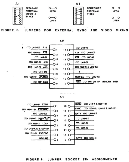
The video section may be set up for either composite external video or separate external syncs and video. As discussed in the set up for the Free Standing Display mode, the output video may also be composite video or separate syncs and video. All cabling in the following descriptions pertains to Digital Group systems.
Composite External Video
Separate External Video and Syncs
Connect the external video to either pin 18 on the back panel connectororVIDEO IN on the paddle card. Thevideo output of the Digital Group TVC is pin 16 of the edge connector in the motherboard. Install the VIDEO jumper on the paddle card ifthe video is connected to pin 18. Connect the horizontal sync to EXHSYN on the paddle card and the vertical sync to EXVSYN. The horizontal and vertical sync outputs of the TVC-64 are pins 12 and 13 respectively on the edge connector. Refer to the TVC pin out in the Appendix for the required signals. Install the jumpers as pictured in Figure 8 for separate external video and syncs. Omitting JPR3 and JPR4 will invert the EXHSYN and EXVSYN signals.This will result in syncing on the trailing edge instead of the leading edge of the sync and the external video will be shifted with respect to the Graphics Display video.
A1
A1
~
SEPARATE
EXTERNAL
0--0
JPR3
~
COMPOSITE
EXTERNAL
0
JPR3
0
VIDEO
&VIDEO
SYNCS
~0
0
[image:10.618.62.553.148.761.2]JPR4
JPR4
FIGURE
8.
JUMPERS
FOR
EXTERNAL
SYNC
AND
VIDEO
MIXING
A2
(TO U4Q-12) A15 (TO U41-1)
16
(TO U4Q-2)
m
A14 (TO U40-10)2 15
(TO U41-2)
m
(TO U4()-4)3 14
(TO U40-8) A13 (TO U41-3J
4 13
(TO U4Q-6)
Ai3
(TO U29-8 & U2Q-13) 5 12 .(TO U41-11) 1
6 11
(TO U26-6)
CP\HtO
~MREa (TO U3Q-12)7 10
(TO U41-6&8)
IIJr
(TO PIN 20 OF ~MORY BUs)8 9
A1
(TO U68-3) EXTH
§'me
(TO U44-1 & U56-13) 1 16(TO U24-12) ~T§V~ SYNC (TO U34--2. U44-2 & U46-12)
•
(TO U3&-12) 2 15EXTV
(TO U68-11)3 14 (TO U34-4)
2C11S-U--4 13 (TO U36-11)
(TO U36-3)
LCU<
(TO U36-9)5 12
(TO U45-4.12 & U34-2)
-,
(TO U36-8) '6 11(TO U32-5) EXTOSC
.7 10
GR~ 8 9 DOTS (TO U45-1)
FIGURE 9.
JUMPER
SOCKET PIN
ASSIGNMENTS
-7-III. THEORY OF OPERATION
The general organization of the Graphics Interface is shown in the Block Diagram in Appendix A. The central section of the unit is a Random Access Memory which receives data from the Central Processing Unit (CPU) and outputs data to either the CPU or a TV Output Circuit. The TV Output Circuit converts the stored data into a video signal which can be displayed on a standard video monitor or TV modified for direct video input. Also contained in the TV Output Circuit are provisions for synchronizing the display with another video signal and superimposing the two on one screen. Control and multiplexing circuits allow the Memory to be accessed by both the CPU and TV display while preventing conflicts. Clock and timing circuits provide memory cycle timing, TV signal ti"ming, and trigger an address counter which tracks the location of the next byte to be di'splayed.
MEMORY
The Memory section consists of 16 TMS-4050 4K Dynamic RAMS (U1 to 16) organized as an 8k block of 8-bit bytes. Refresh is accomplished by the continuous reading of data to be displayed. In order to expedite refresh, one bank of 8 RAMS (U1 to 8)contain all EVEN addresses and the other bank of 8 RAMS (U9 to 16) contains all ODD addresses. Using this scheme, the 128 memory accesses required to refresh all 64 rows of both banks represent 41ines of displayed data. Since the duration of a display line is approximately 63.6 micros-econds (a time fixed by the standard TV sweep frequencies), a complete refresh occurs in 0.254 milliseconds, considerably more often than the required 2 milliseconds. Data from the CPU is buffered by the 7401 data buffers (U37 &38) and applied to the memories. Since the TMS 4050 uses open-collector multiplexed I/O, a Data Enable (DE) is applied to the data input buffers to ensure they are enabled only when a memory write is to be performed. Both banks of the memory are fed in parallel by the data buffers but there is no conflict since both banks are never enabled simultaneously. Note that since the 7401 buffers invert the incoming data, all data is stored inverted and must be re-inverted after being read. Data read out from the memories is buffered by the 7400 data buffers (U25 & 47) and fed to the TV display 74165 shift registers (U48 & 49) and the 74173 CPU data output latches (U58 & 59). A signal (WHITE) applied to the 7400 data buffers will force the output of the buffers to be all1's if WRiT'E=0. The purpose of this signal will be seen later. The memory address lines are driven by four 74367 tri-state buffers (U50, 51,60, & 61). U51 & 61 are enabled when 5i'SP=0 (i.e. DISP=1) allowing signals from the display address counter to be applied to the memory address lines. It will be seen later that the condition DISP=1 means that a memory cycle is to be performed to retrieve data for the DISPLAY. When DISP=0(and consequently DISPBUF=0) a CPU read or write cycle is to be performed; therefore, U50 & 60 are enabled, applying address signals from the CPU to the address lines of the memories. The derivation of the signals CEODD, CEEVEN, and R/W will be discussed in another section.
CLOCK, TIMING GENERATION, AND ADDRESS COUNTER
The clock frequency required is determined by the data rate which will produce the desired display on a TV monitor utilizing U.S. standard Vertical and Horizontal frequencies. Each data line is 46 Bytes long (3 bytes for a sync pulse, 5 bytes for a left margin, 32 bytes of data, and 6 bytes for a right margin). Therefore we have (based on 262 lines/frame):
Frame Time = (1/60) sec = 16.667msec (Vert Sweep = 60Hz)
Line Time = (1/60)(1/262) sec = 63.613usec (Horiz.Sweep = 15.72kHz) Byte,Time = (1/60)(1/262)(1/46) sec = 1.3829 usec
Bit Time = (1/60)(1/262)(1/46)(1/8) sep = 172.86nsec (5.784960 MHf )
The required data rate is 5.784960 MHz. A crystal twice this frquency is uSj3d to generate CK1 =11.569920 MHz and then divided by two to achieve CK2 at the appropriate frequency. Signals CK1 a'ld CK2 are used to clock and enable a counter chain (U33, 39, 52, 53, 62, & 63) which supplies the memory address used when a DISPLAY data fetch memory cycle is to be accomplished. U33, 52, and 62 may be thought of as the "Line Counter", ke1eping track of the number of the line currently being displayed. I.C.'s 39, 63, and the most si9,nificant bit of U53 may be tho!-l9ht of as the "Byte Counter", keeping track of the next data byte to be displayed. The Byte qounter is always one count anead of the data byte currently being displayed because it is used to fetch the next data byte from memory before it is requjred. (Note that "Byte 0" on any line is the first DATA byte, NOT the first byte of the line whiCh would occur during the syrc pulse, and NOT the first byte of the margin, either). The three least-significant bits of U53 are the "Bit Counter" and represent the data bit currently being displayed.
~ I
Control Section
The control section determines when a memory cycle is required by the CPU or the display, sequences the requests to avoid conflicts, and issues appropriate control and timing signals. Control of the memory is allocated to either the Display or the CPU by aD-type 7474 flip flop (1/2U28) whose outputs are designated DISP and
i5'iS'P~
The DISP signal is active when the Display is in control of the memory and, conversely,D'i'SP
is active when the CPU is in control of the memory.A CPU memory cycle begins when the high order address lines (A 15, A 14, and A 13) are addressed in the pattern selected by the address blo,ck select jumpers, Tilese signals are applied thru the address select jumpers to a 7430 NAND gate (U41). Certain other signals are also fed to U41 and must be present to initiate a CPU cycle. REFRESH is gated in to assure that Z-80 refresh cycles do not trigger an unnecessary cycle. A 16 is an extra "high order address line" and essentially serves as an externally driven "board select" line to allow the board to be enabled or disabled at will. Both REFRESH and A 16 are tied to +5 thru pullup resistors so they are not affected when not in use. MEMREO 'is inverted and gated to U41 in the case of Z-80 systems as is the composite of MEMRD and MEMWR for 8080 systems. Optionally, ROM can be gated in thru a jumper to allow a ROM to overlap the onboard memory without conflict. When the appropriate signals are present, CPUREO'is made / low, indicating the CPU has requested a memory cycle. The falling edge of CPUREO sets U31, % of a 7473 J-K flip flop, bringing COMPREQ high. COMPREO is applied to the 0 input of a 7474 (U28) and, if CEis high (i.e. CE is low indicating that a memory cycle is not currently in progress) the next rising edge ofCK2will set
DiSP
high, giving memory control tothe CPU. In the eventCE
is low, a memory cycle is in progress and control of the memory cannot be shifted to the CPU until the cycle is completed. Once DISP becomes high, a series of gates applies a HOLD Signal to the CPU card thru pin 20. When 30 becomes high, U31 is reset, driving COMPREO low. AfterCE
returns high (indicating completion of the CPU memory cycle) U28 will switch on the next rising edge ofCK2
and control of the memory will automatically revert to the Display.A Display memory request is generated by making DISPREO high on the next falling edge of
00
after BIT0, BIT1, and BIT2 become high simultaneously. DISPREO is cleared by the occurrance of 20 while DISP is high.Once a CPU or Display memory cycle has been requested by making CPUREO or DISPREO high. a Cycle Start (CS) signal will be applied to the 74195 shift register (U21) and a memory cycle will begin. The gating (U20. and 27) will cause the memory cycle to be two CK2 cycles long for a Display Read and three CK2 cycles long for a CPU Read or Write.
DATA OUTPUT LATCHES
Output data to the CPU is latched in two 74173tri-state 0 Registers. These registers are selected when DISP is low and data is clocked into them by 30. The tri-state outputs are enabled onto the data bus by CPUREO being low.
TV OUTPUT CIRCUIT
Data to be displayed is loaded alternately into U48 and 49, the 74165 shift registers. depending on whether B0 is 1 or 0 (except that no data is loaded when BEris low indicating the margin of the picture. The data is then shifted out of the appropriate shift register by
CK2.
The data from the shift registers (OHSR1 and OHSR2) is gated into the output circuit unless the terminal GRAPH is pulled low, disabling the display of graphics. If the terminal DOTS is not grounded,CK"2
is gated to the output breaking up horizontal lines into a series of dots to prevent horizontal lines from appearing brighter than vertical lines. Comparator U24 separates an external video signal into high and low levels which can be superimposed on the screen by-'
bringing EXTVID high. The entire picture can be inverted by bringing INV low or can be blacked out by bringing BLACK low.
TV Synchronization
The Graphics Display provides all the signal processing necessary for TV synchronization forthe various modes of operation including composite video output, separate video and sync output, composite external video, separate external video and sync, and no external video.
Horizontal sync pulses are provided by a one-shot with a 5us pulse width (U34) which is triggered by RSS, the reset to the bit counters (U53, U63), RSB is generated when the bit counters reach the end of a line or an external horizontal sync occurs. The horizontal sync is applied to the circuit consisting of U43 and U56 which produces a serrated sync to ensure that horizontal sync is maintained during vertical retrace. In the composite video output mode, the serrated sync is fed to an inverter (U23) through JPR1 to produce active low pulses and added to the video through JPR5.1f separate output video and syncs are being employed to the Data Monitor, the noninverted serrated sync is connected to the horizontal sync input of the monitor. When an external video signal is input to the Graphics Display, an RSB is generated each time a horizontal sync pulse is detected by the sync separator circuit.
-9-Vertical sync is provided by the line counter chain (U52,U62 and U33). -9-Vertical sync occurs when lSgoes high as a result of the line count reaclling 256 or an external vertical sync pulse is detected forcing L8 high. L8 is fed to U56 to provide serrated sync to be added to the video in the composite video output mode. Forthe separate video and syncs output mode, L8 is fed to an inverter (U23) through JPR1. The resulting L8 is connected to the vertical sync input of the Data Monitor. JPR5 is removed to omit sync pulses from the video output.
When composite external video is employed, the external video is fed to a comparator (U24) which removes the video and produces active low pulses corresponding to the external sync pulses. These pulses are inverted and fed to the D input of U46, the D input of U36 through the jumper between pins 3 and 15 of A 1 and to the positive going trigger input of a one-shot with a 20us pulse width (U34). The horizontal and vertical sync pulses are separated by clocking the pulses through U46 and U5? to obtain an AUXRSB for each horizontal vertical sync pulse and clocking U36 with the rising edge of the active low 20us pulse. Since U36 is clocked 20us after the start of a sync pulse, only the vertical sync will be long enough to allow an AUXRSL to be generated. AUXRSL is fed to U6? to reset the line counters and to U33 to force L8 high and begin the vertical sync. The clears to U46 and U5? prevent generating more than one RSB for each external sync.
-For the separate external video and sync mode the horizontal sync (EXHSYN) is fed to U68 and, for positive horizontal sync pulses, inverted by omitting JPR3. The horizontal sync generation is then the same as for composite external video. The external vertical sync (EXVSYN) is applied to another section of U68 and inverted for negative sync pulses by omitting JPR4. These pulses are then fed to the D input of U36 through the jumper between pins 3 and 14 of A1. U36will now be clocked by LCLK through the jumper between pins 5 and 13 of A 1. Now AUXRSL will be generated at the end of the line following the start of the external vertical sync pulse.
Light Pen Circuitry
Light is detected by the phototransistor (Q1) and converted to active low pulses which trigger a flip-flop (U5?) to produce the signal FOUND. FOUND latches the present values of the line and bit counters into U54, U55, U64 and U65. U55 and U641atch the line count and the tri-state outputs are enabled when PSEL (3 is high and PSEL 1 is low. U66 is a tri-state buffer that is enabled when PSEL 1 is high. Enabling U66 allows the status of FOUND,
SW,
L8 and B5 to be input to the CPU. In addition to enabling the tri-state latches, PSEL (3 clears U5? when pulled low to ensure that FOUND is high only when light has been detected. PSEL 0 is also inverted and fed to U35 along with ~ to generateB'i:'AC'K
which will black the screen.IV. SPECIFICATIONS
Display Area Square, 256 x 256 point display, 65,536 points total.
Memory 8K bytes on-board. This memory can be used for programs or data when not being used for graphics. External Sync Inputs for synchronizing to an external devise. Outputs for synchronizing an external device such as the
TVC-64 or the Digital Group Data Monitor. Graphics
Boards per system Video Mixer Light Pen Req u i rements:
Power
Unlimited.
Selects TV readout, graphics, or superimposed.
Pen location to one dot resolution with software supplied.
+5V at 1.5A +12V at .3A -5V at 5ma Video Monitor
One Output Port to command board options
One Input Port to accept Light Pen data and board statu~
V.CONSTRUCTION
A. Graphics Display Board
1. Refer to the Parts List and Parts Layout in the Appendix when assembling the Graphics Display. Ensure all the components are present.
2. Insert the one 8-pin, thirty-three 14-pin, twenty-four, 16-pin and sixteen 18-pin IC sockets. Place a book orotherflat object over the sockets and invert the board. Carefully solder all pins, being alert not to cause "solder bridges" between pins or nearby traces.
3. Cut the tabs on the crystal holder as indicated in the Crystal Socket Preparation Detail below. Solder the crystal socket in place.
CRYSTAL SOCKET
PREPARATION DETAIL
4. Solder the two 220 ohm, 1 watt resistors in place. Cut the leads close to the board.
5. Solder the sixteen .01 ufd disc bypass capacitors in place. Cut the leads close to the board. 6. Solder the eight .1 ufd disc bypass capacitors in place. Cut the leads close to the board.
7. Insert and solder the two .001 ufd disc, one 750 pfd, five 1 ufd and two 4.7 ufd capacitors. Note the polarity for the 1 ufd and 4.7 ufd capacitors marked on the board. The positive lead is marked by a + sign or a blue dot. Cut the leads close to the board.
8. Insert and solder the sixteen V4W resistors. Cut the l!3ads close to the board. R21 is not included as this is an optional part for use on systems without a -5V supply.
9. Insert and solder the two 5K ohm variable resistors. Be sure the slots for adjusting are toward the top edge of the board. Cut the leads close to the board.
10. Insert and solder CR1 (1N4148). Cut the leads close to the board.
11. Insert and solder the 75 ohm, 114 watt resistor (Rt) in the paddle card. This resistor terminates the video. Cutthe leads. 12. Measure the resistance between each power supply voltage pin and ground. Ground is pin 2 ofthe edge connector, +5V is pin 1, +12V is pin 36, -5V is pin Band":' 12V is pin R. +5V will read approximately 200 ohms on a DVM or a VOM on Rx10 or greater. The others should read 400 ohms or greater.
-11-13. Install the crystal and all IC's except the memory chips. Plug the board into your system and check the supply voltages on the board. Check that +12V at the memory chips is on pin 10 only, -5Von pin 1 and ground on pin 18. This step may prevent damaging the memory IC's.
14. Refer to the set up and operation section and install the address and video jumpers. For the initial chek out, jumper the address to an unused memory area.
15. Install the memory IC's and test the memory by running a memory test program or by using a memory editor. If the board fails the memory check, refer to the Troubleshooting Section.
16. Check that the video is synchronized and that the control bits (G raph, INV, etc.) operate properly. Refer to the Troubleshooting Section if any problems are encountered.
B. Light Pen
1. Refer to the Parts List and Parts Layout in the Appendix. Ensure that all parts are present. 2. I nsert and solder the ten %watt resistors. Cut the leads close to the board.
3. Insert and solder the one 1 ufd tantalum capacitor. Note the polarity marked on the board. The positive lead of the capacitor is marked by either a + sign or a dot. Cut the leads close to the board.
4. I nsert and solder the two .033 ufd disc capacitors. Cut the leads close to the board.
5. Insert and solder the one 2N5139 and two 2N5129 transistors. Cut the leads close to the board.
6. I nsert and solder the LED. Orient the cathode toward the bottom of the board. (The cathode is marked by a notch in the body of the LED or by a longer lead). The anode is connected to +5V. Seat the body of the LEO against the circuit board, otherwise it may contact the Light Pen case cal,.Jsing misalignment of the circuit board inside the tube. Cutthe leads close to the board. I
7. Refer to the Light Pen Construction diagram in Figure 10 before installing the phototransistor.lfthe phototransistor is installed too close to the circuit board, the operation of the Light Pen will be effected since detection of light as it passes over the hole in the end cap is diminished. The emitter lead (nearest the tab) is connected to hole number 2, the base to the center hole, and the collector to hole number 1.
8. Insert and solder the pushbutton switch. Seat the switch against the circuit board.
9. Solder one end of the cable to the holes (3 through 6) at the end of the board. Secure the cable to the board with a small cable tie.
10. Push the free end of the cable through the hole in the flat end cap so that the smaller diameter section is toward the circuit board. Refer to the Light Pen C~:>nstruction in Figure 10.
11. Slide the Light Pen body over the circLlit board. Align the small hole in the side of the body over the switch. 12. Insert the 3/16" roll pin in the pushbutton. Insert the other end of the roll pin into the hole in the top of the switch so
that the pushbutton has freedom of movement in the hole of the Light Pen case.
13. Carefully place the rounded end cap ov~r the phototransistor. Ensure that the transistor is parallel to the plane of the circuit board and centered within the opening in the end cap. The tap on the transistor may need to be cut for full penetration into the end cap. Align the' slot in the end cap with the circuit board.
14. Push the flat end cap into the Light Pen body.
15. Refer to the Parts Layouts for the Paddl~ Card and Light Pen in the Appendix. Identify the wires in the cable by signal name as they were connected to the Light Pen. Solder each wire to the corresponding point on the Paddle Card. 16. Check the Light Pen operation using th~ Calibrate routine in the Appendix. If the operation is not correct, refer to the
I
IP
IE
7/16 n:>i [image:16.798.22.765.122.552.2]VI. TROUBLESHOOTING
A. General
Most problems with printed circuit boards are caused by construction errors. Therefore, the first step is to double-check all components for proper values. check for bent IC pins and solder bridges or splashes. Another problem source could be improper jumper configurations. Refer to the Set Up and Operation section and verify that all jumpers are proper for the mode of operation.
If no construcion errors are found. determine what area is malfunctioning and refer to the Block Diagram in the Appendix to determine associated areas that effect the problem area. The schematic is divided into areas corresponding to the functional blocks in the block diagram as an aid in troubleshooting. Reading the Theory of Operation and the Set Up and Operation sections and studying the Block Diagram and Timing Diagrams should enable you to find nearly any problem.
B. Memory Errors
1. Refer to the Block Diagram to determine the areas that effect the memory. 2. Check the clocks, CK1 and CK2. CK1 is 11.569 MHz and CK2 is 5.785 MHz. 3. Check for CPUREQ at U32. Ensure that the address jumpers are correct. 4. Check for chip enable (CE. CEEVEN. CEODD) and R/W.
5. Check the timing of B1-L7. These form the memory address during display and refresh. 6. Check DE to ensure the data to memory is being enabled.
7. Ensure that
W'HiTE
is high or the data from memory will always be FFH.c.
Video Output Problems1. Refer to the Block Diagram to determine the areas that effect the video output. 2. Check that GRAPH is high or the display data will not be enabled to the video output. 3. Check the signals at U23. U27, U42, U43, and U68 in the video output circuit.
4. Check the inputs to and outputs from the shift registers.
D. Horizontal Sync Problems
1. Refer to the Block Diagram for areas that effect horizontal sync.
2. Check the sync generator circuitry for a 5us pulse at pin 12 of U34, RSB at pin 9 of U34 and B4, B5 and L8 at U56. 3. Ensure that the serrated sync is present at pin 8 of U56.
E. Vertical Sync Problems
1. Refer to the Block Diagram to determine which areas effect vertical sync.
2. Check for L8 at U56 in the composite video mode and L8 at pin 13 of U23 in the separate syncs mode. 3. Check the counter chain (L0-L8).
F. Sync Separator Problems (External video modes only)
1. Refer to the Block Diagram to determine the areas effecting the sync separator. 2. Ensure that the jumpers are correct for the mode of operation.
3. Verify that AUXRSB and AUXRSL are being generated.
4. Check that the 20us pulse is present at pin 4 of U34 and pin 11 of U36 in the composite video mode. 5. Check that LCLK is present at pin 11 of U36 in the separate syncs mode.
6. Check for SYNC at pin 12 of U46 and pin 12 of U36.
G. Light Pen Problems
1. Refer to the Block Diagram to determine which areas effect the Light Pen circuitry. 2. Verify that LIGHT is present at pin 5 of U57 and FOUND is generated.
3. Check that Bit 0-L7 are present at U54, U55, U64, and U65.
4. Check that PSEL 0 and PSEL 1 are present and the 74173's are being enabled. 5. Check the status inputs and outputs at U66.
6. Ensure that the phototransistor is centered in the end of the Light Pen.
-15-VII. APPENDIX
A. BLOCK DIAGRAM
B. TIMING DIAGRAMS
C. SAMPLE SOFTWARE ROUTINES
D. PARTS LIST
1. Graphics Display 2. Light Pen
E.
DIGITAL GROUP BUS PIN ASSIGNMENTS1. Memory Bus 2. I/O Bus 3. TVC Pin Out
4. Back Panel Connector Pin Out
F. CABLING DIAGRAMS
1. Graphics Control Cable Wire Diagram 2. Graph Input Cable Wire Diagram 3. Cable Orientation Diagrams
G. PARTS LAYOUT
1. Graphics Display Board 2. Light Pen
H. SCHEMATICS
I
..
-.JI
; -~ ADDRESS
\ / PROM CPU
ADDRESS "MULT 'PLEX ING
PSILO PS£L 1
"0
/\
TIMING LOGIC
\/
LIGHT
PEN
LOGIC
STATUS
f4
--
-A16
0
MEMORY
CONTROL LOGIC
t
LIGHT PEN
H
BUS CONTROL SIGNALS
EXTERNAL SYNC
-
-DATA BUFFERS
TO ALL BLOCKS
SYNC SEPARATOR
A.
GRAPHICS DISPLAY, BLOCK DIAGRAM
--->
VIDEO OUTPUT CIRCUITRY
-SERIALIZER
1---,1-. . . . MONITOR
-WHITE -. EXTVID
'---4'U~ GRAPH INV
8.1
MEMORY CYCLE TIMING
CK1
CK2
CS
I
CE
"
,<
20
n
30
_______________________
~'r~'---r-I~---n i L
MEMORY CYCLE
=
Two CK2 CYCLES MEMORY CYCLE=
Three CK2 CYCLESB.2 BIT COUNTER TIMING, BITCJ-BCJ
CK1
CK2
BITIil
BIT1
~
BIT2
CYIil
n
---~
~---B.3 BIT COUNTER TIMING, B1-B5, RSB GENERATION
CYIil
I
I
I
U
I
~
I
~
I I I
~
I I I I I I I I
LLL
B1
B2 --,
----rL
B3..J
---I
B4
.-J
_____ ----'I
8.4 LCLK GENERATION
8.41 ... _ _ ...
85
--,~
_ _ _ _ _ --"u
U
L
L
LC~
... _ _ _ _ _ _ --"'----_ _ _ _
IL
B.S
LINE COUNTER TIMING, LGl-L3
L0
L11
... _ _
....
L2
1 ... _____
--'
L31
... ________________
~----~
CY
(~
.... _ - - - -_ _ _ _ _ _ - - - . . . . , . _ - - - 'B.6 LINE COUNTER TIMING, L4-L8, VERTICAL SYNC GENERATION
CY (U62)
Jl
n
n
n
nJ1
n
n
n
n
4.4..L4
l
II
I
--~
--l
II
L5
_N
L6
J
II
! ~
--, --.~
II
L7
-
.-nn
CY(U52)
. 'J
La
n
VERTICAL SYNC
-. - -~ --., -
-19-B.7 HORIZONTAL SYNC GENERATION-NO VERTICAL SYNC
B2
1 ___ ----..
L..--_----'n ... __
...I B4B5
~---~I---~---~H~'---~
II
RSB ---~u
5us
La
HORIZONTAL SYNC
B.8 HORIZONTAL SYNC GENERATION DURING VERTICAL SYNC
B2
--______ n ... __ ...
84
I
85
RSB
u
5us
La
HORIZONTAL SYNC
B.9
SERRATED SYNC
"
'I
"
If
I
START VERTICAL SYNC I I
L
~~
__
~n~_
U
~~~
_____
~
I
I
c.
SAMPLE SOFTWARE ROUTINES
SOFTWARE INSTRUCTIONS
The Digital Group Graphics Board is supplied with the Basic software routines needed for plotting dots and lines. These routines will run with Basic or independently.
The Graphics Board is a bit mapped video device. Therefore each dot appearing on the screen is an address in memory serially fed to the video.
We have already written for you the algorithms necessary to convert these addresses into singly addressable coordinates. That is, to put a dot on the screen in the spot you want to, you do not have to find the sixteen bit address and enter a number with the appropriate bit on in it. Instead, you place two eight bit numbers in
"x"
and"v" ,
a one in the "DE" and call "GETVAL" . The following routines are on the tape you received with your board:VALUE: Variable that pOints to the routine that you want to execute. All routines are called via the variable "VALUE", simply by placing the appropriate number into the "DE" register pair. Therefore these routines can be used with Basic or independently. These routines must be called via "GETVAL" or the stack will be destroyed .
.. THE VALUE "0" Turn off dot.
• THE VALUE "1" Turn on dot.
.. THE VALUE "2" Compliment the dot (invert).
THE VALUE "3" Test the dot. Test returns a value in the HL register of fa if dot was off,non 0 if dot was on.
• THE VALUE "4" Plot a line with the dots off .
• THE VALUE "5" Plot a line with the dots on.
THE VALUE "6" Calibrate the light pen.
THE VALUE "7" Continuously draw with the light pen.
THE VALUE "8" Locates the light pen and returns the two "X" and "Y" values.
~ THE VALUE "9" Clears the graphics buffer .
• THE VALUE "10" Initializes the 10 to the Graphics Board.
-21-Descr1ption of each function
1. POINT: A"ows you to plot single dots by an INVERTED CARTESIAN COORDINATE system, i.e. X=0 to 255 and V=0 to 255.
"x
(0) " being the left hand side of the screen,"x
(255) " being the right hand side of the screen and"v
(0) " being the top of the screen,
"v
(255) " being the bottom of the screen. EXAMPLE:•
X(O), Y(O)
X(255), Y(255)
•
To place a dot at the coordinate you wish, you first have your program deposit the values for
"x"
and"v"
in the specified temporaries for point, place a one into the "DE" register, and call "GETVAL".2. PLOT: Allows you to plot a line from one point on the graphics screen to anonler, E.G. Xl, Vl to X2, V2. X1 being the starting value horizontally, V1 being the starting value vertically. So therefore X2 is the ending value horizontally and V2 the ending value vertically.
EXAMPLE:
X1, Y1
X2,Y2
3. CLEAR: Clears the screen.
4. CALIBRATE LIGHT PEN: This routine is set up to allow you to calibrate the tight pen accurately to your own needs. More specifics on this routine are mentioned further on in the text.
5. LOCATE LIGHT PEN: Supplies the necessary software needed to interpret the location registers on the graphics board. This routine in turn can be used in conjunction with POINT or PLOT. The pen location is returned in "X" and "Y".
6. INITIALIZE: Sets up the Graphics Board 10. Documentation on the port assignments is in the hardware description. The board has an input socket that is plugged into a standard 10 port. A hex FF will initialize the board so that you may see the graphics buffer.
Each of the routines listed here except "LOCATE", have their own set of variables that need to be set before calling.
POINT, PLOT and CLEAR all have to know where you have jumpered the graphics memory. It Is critical that you set "GRFST" (graphics start), before you execute any of these routines!!!
For example, if you have jumpered the board for 8000 Hex, you will go into the monitor, go to the address that "GRFST" is and set it to "00 80". At that point all the routines know where your board is located. This can also be accomplished in Basic with the FILL command. The difference is Basic uses the decimal equivalent of the hexidecimal number mentioned previously.
USING THE CALIBRATE LIGHT PEN ROUTINE
Set "GRFST" to the location at which your board is jumpered. Least significant byte first, most significant byte last! Place a "6" into the "DE" register and call "GETVAL". A dot at the coordinates "80-80/HEX", the middle of the screen, will appear.
To calibrate the pen to place a dot under the pen, place the pen on your monitor screen over the dot, then press the button. The screen will then flash white, and adjust the brightness and contrast for the differences inherent in your monitor.
By adjusting the brightness and contrast on your monitor you can fine tune for best results. The following is a list of all the variables and their functions:
GETVAL=(060D)
GRFST=(08CB)
X=(08C5)
Y=(08C7)
X1 =(08C9)
Y1 =(08CA)
X2=(08F1)
Y2=(08F2)
VALUE=(08C3)
XOFF=(08D2)
YOFF=(08D1 )
Start of Graphics routines. You must always enter here by placing a value into the "DE" register and calling this address.
Page the graphics buffer starts on. All routines use this location.
Horizontal parameter for point routine.
Vertical parameter for pOint routine.
First horizontal parameter of line for plot routine.
First vertical parameter of line for plot routine.
Second horizontal parameter of line.
Second vertical parameter of line.
Flag that vectors to the subroutines.
X offset for calibrate light pen routine.
Y offset for calibrate light pen routine.
The 10 port assignments forthis software are 7 for IN and 7 forOUT. These ports are used forthe light pen registers and controlling the Graphics Board functions via software.
You do not need to hook up 10 cables to your board if you don't want these functions. If you do andyou don't have ports atthe given locations you must change the port assignments in the software using the listing supplied.
Here are a few basic programs as examples:
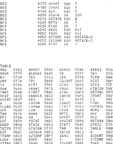
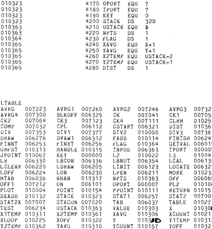
-23-HEX ROUTINES
Cassette Routine Parameters
READ 600-8FS
NOTE:
0600
0100
ST
0600H
0600 C9
0110
RET
The tape supplied with the Graphics Board contains0601 00
0120
NOP
the code to be inserted from CJ6CJCJH to CJSFFH in0602 00
0130
NOP
MAXI BASIC. This can be done in the AUDIO0603 C9
0140
RET
version by changing the starting address located at0604 00
0150
NOP
c.J118H toaaH,
a119H to a6H, and the ending0605 00
0160
NOP
0606 C9
01'70
HET
address ata
11 AH to FFH and CJ 11 BH to aSH. After0607 00
0180
NOP
the code has been read into the correct locations, a0608 00
0190
Nap
new cassette can be written that will contain the new0609 C9
0200
HET
code as well as MAXI BASIC by option 2, WRITE060A 00
0210
Nap
CASSETTE.0608 00
0220
NOP
060C C9
0230
HET
0600 ED 53 C3 08
0240 GETVAL LD
(VALUE),DE
0611 21 11" 06
0250
LO
HL,TAB
0614 3A C3 08
0260
LO
A,(VALUE)
0617 CB 17
0270
RL
A
0619 85
0280
ADO
L
061A 6F
0290
LD
L,A
Ob18
30 01
0300
JH
N C, ~lTAB0610
24
0310
'INC
H
061E E9
0320 MTAS
JP
(HI..)
0611" 1C3 14
0330 TAB
JR
Off
0621 18 1£
0340
JH
ON
0623 18 25
0350
JR
CPL
0625 18 '(5
0360
Jl<
TEST
062'{ 18 68
0370
J~LOr'!:,'
0629
18
60
0380
JH
LUN
0628 18 213
0390
JH
LCAL
0620
18
~60400
JR
LDRAW
0621:" 18
~80410
JH
LfJEN
0631 18 5D
0420
JR
LCLEAR
0633 ' 18 1£
0430
JR
LINIT
0635 CD 6C OC3
0440 OFF
CALL POIIfT
0638
3A
CD 08
0450
LO
A,(HANDLE)
063B 4F
0460
LD
e,A
063C 78
0470
LD
A,B
063D 2F
0480
CPL
Ob3E
Al
0 490
AND
C
0631:" 18 66
0500
JR
fINISH
06!!1 CD 6e 08
0510 ON
CALL POINT
0644 3A CD 08
0520
LD
A,(HANDLE)
06 47 BO
0530
OR
B
0648 18 5D
0540
JH
FINISH
064A CD be 08
0550 CPL
CALL POINT
0640 3A CD 08
0560
LO
A, (HANDLE)
0650 A8
0570
XOR
B
0651 18 54
0580
JR
FINISH
0653 3E
FF
0590 LINIT
LD
A,OFFH
0655 D3 07
0600
OUT
OPORT
0657 C9
0610
RET
0658 97
0620 LCAL
SUB
A
065F 3E tlO
0650
LO
A,SOH
0661 32 C6
O~0660
tD
(X+l) ,A
0664 32 C8 08
06'70
LD
(Y+l),A
0667 CD 41 06
0680
CALL ON
066A CD AF 06
0690
CALL STATl
066D CD Dl 06
0700
CALL LOCATE
0670 3A C8 08
0710
LD
A,(Y+l)
0673 C6 80
0720
ADD
80H
06'75 ED 44
0730
NEG
06'rr
32 Dl 08
0740
LO
(YOfF),A
067A 3A C6 08
0'750
LD
A, (X+1)
0670 C6 80
0760
ADD
80H
067f ED 44
0'"(70
NEG
0681 32 D2 08
O~r80
LD
(XOFF) ,A
0684 C9
0790
RET
0685 CD BE 06
0800 LDRAW
CALL DRAW
0688 C9
0810
RET
0689 CD AF 06
0820 LPEN
CALL STATl
068C CD Dl 06
0830
CALL LOCATE
068F C9
0840
RET
0690 CD AC 08
0850 LCLEAH CALL CLRM
0693 C9
0860
RET
0694 CD Oll 08
08'rO
LOff
CALL PLOT
069'7 C9
0880
RET
0698 CD 04 08
Otl90 LON
CALL PLOT
069B C9
0900
RET
069C 3A CD 08
0910 TEST
LD
A,(HANDLE)
069F BO
0920
OR
B
06AO 62
0930
LD
H,O
06Al 6F
0940
LO
L,A
~')6A2
28 OA
0950
JH
Z,FINYT
06All 2C
0960
INC
L
06A5 18 07
0970
JR
fINYT
06A7 2A CF 08
0980 fINISH LO
HL,(NHAN)
06AA 77
0990
LD
(HL) ,A
06AB 2A C3 08
1000 FINNT
LD
HL, (VALUE)
06AE
cg
1010 FINYT
RET
06Af DB 00
1020 STATl
IN
KEY
06Bl FE 91
1030
CP
91H
06B3 C8
1040
RET
Z
0684 FE 83
1050
CP
83H
06B6 C8
1060
RET
Z
068'( DU 0'(
10'(0
IN
IPORT
0689 CH 6'(
1080
BIT
ll,A
06B8 20 F2
1090
JR
NZ,STATl
06BD C9
1100
RET
06BE DB 07
1110 DRAW
IN
IPORT
06CO CB 6'(
1120
BIT
U,A
06C2 20 06
1130
JH
NZ,DRAW1
06C4 CD 01 06
1140
CALL
LOCATE
06C7 CD U1 06
1150
CALL
ON
06CA DB 00
1160 DRAWl
IN
KEY
06CC FE 91
11'( 0
CP
91H
06CE C8
1180
RET
z
06CF 18 ED
1190
JR
DRAW
06D1
1200 LOCATE EQU
$
F6D1 3E FE
1210 CSTART LD
A,OFEH
CLR fOUND,STROBE STATUS,WHITE
06D3
1220
*
Off,LED OFF,BLACK ON
0603 03 07
1230
OUT
OPORT
06D5 3C
1240 BLKOfF INC
A
BLl1CK OFF
-25-06D6 D3 07
1250
OUT
OPORT
06D8 DB 07
1260 L8
IN
IPORT
06DA CB 77
1270
BIT
6,A
L8=1'"1
06DC 28 FA
1280
JR
Z,L8
060E 3E 7B
1290 L8CON
LD
A,7BH
06EO
~30'(
1300
OUT
OPORT
06E2 5F
1310
LD
E,A
06E3 06 00
1320
LD
B,O
INITIALIZE
COUNT
06E5 OE 07
1330
LD
C,IPORT
06E7 16 40
1340
LD
D,40H
L8 MASK
06E9 21 F2 08
1350
LD
HL,USTACK-l
06EC
1360
*
06EC
1370
*
06EC
1380
._******
LOOK FOR RETRACE TIME
.****~h•••
06EC DB 07
1390 L8NOT
IN
IPORT
06E£ A2
1400
AND
D
06EF 20 FB
1410
JR
NZ,L8NOT
06Fl 18 11
1420
JR
STAT2
06F3
1430
1Hdt***GET LIGHT PEN LOCATIONS ********
06f3 3E 78
1440 INPOS
LO
A,78H
06F5 D3 07
1450
OUT
OPORT
06f7
ED
AA
1460
IND
06F9 3C
1470
INC
A
STROBE 01
06FA D3 07
1480
OUT
OPORT
06fC ED AA
1490
IND
06fE 3E EO
1500
LD
A,OEOH
·0700 90
1510
SUB
B
0701 CA D1 06
1520
JP
Z,CSTART
0704
'lE
1530 STAT2
LD
A,E
STATUS STROBE
0705 D3 07
1540
OUT
OPORT
0'"(07 ED 78
1550 STAT2X IN
A, (C)
0709 FA F3 06
1560
JP
M,INPOS
FOUND=l?
070C A2
1570
AND
D
NO,L8=1?
070D CA 07 07
1580
JP
Z,STAT2X
NO
0710 3£
'ff1590 STXCON LD
A,7FH
0712 D3 07
1600
OUT
OPORT
0714 3E F9
1610
LD
A,OF9H
0716 88
1620
CP
8
0717 FA Dl 06
1630
JP
M,CSTART
071A
1640 ._**** INITIALIZE TO COMPUTE DOT LOCATIONS ******
071A 78
1650 COMP
LD
A,B
CALCULATE NUMBER Or POINTS
0718 CB
2F
1660
SRA
A
0'( 1 D 2F
1670
CPL
o'r
1 E 32 F3 08
1680
LD
(NPTS),A
0721
1690
*
lvtOST X CORD 00---, OR
11---0721 21 EF 08
1700 CK
LD
HL,USTACK-4
0724 3A F3 08
1710
LD
A,(NPTS)
0727 47
1'{20
LD
B,A
0728 OE 00
1730
LD
C,O
072A 7E
1740 CKl
LD
A, (HL)
0728 £6 CO
1750
AND
OCOH
072D 28 05
1760
JR
Z,CK2
072r~