THE SIMULATION OF TRANSPORT DELAY WITH THE HYDAC* COMPUTING SYSTEM
ABSTRACT: A general purpose hybrid computer program for the simulation of transport delay is described. The program utilizes a combination of analog and digital components in the EAI HYDAC Com-puting System to provide a high speed, multichannel variable delay capability. A standard expanded Digital Operations System of the HYDAC Computer can provide up to ten (10) channels of variable transport delay.
BACKGROUND
The need to simulate a transport delay arises frequently in analog computation, occurring as the solution of the flow equation and the wave equa-tion, both partial differential equations. More explicitly, the realistic simulation of systems involving the flow of liquids and gases in pipes or the propagation of electric or acoustic waves requires the representation of the transport de -lay phenomena. A standard analog computer ap-proach to simulation of time delay is to employ a linear computer circuit, for which the ideal·
delay transfer function has been approximated by a ratio of polynomials (often referred to as PadJ polynomials). A typical approximation, by fourth degree polynomials, is illustrated by the circuit of Figure 1. In this case, a single channel of
FIGURE 1: Analog Computer Circuit for Representing Trans-port Delay Using 4th Order Pad; Approximation
delay employs six amplifiers and twelvepotentiom-eters to produce a fixed delay, TD, where the maximum allowable value of T D for a one degree phase error in a one cycle per second signal is 1.2 seconds(I). For a ten cycle per second signal, the maximum allowable delay for a one degree phase error is 0.12 seconds.
1
Although widely used, this approach to transport delay simulation suffers from two basic limita-tions: 1) since large phase errors occur at high frequencies, rapidly changing and discontinuous functions can not be represented realistically; and 2) variable time delays, as with the simula-tion of variable fluid velocity, requires a large number of multipliers and hence becomes un-economical.
An alternative approach for transport delay simu-lation employs sampling of the analog signal, storage of the discrete sampled values in a fixed number of memory cells, and reconstruction of a stair-step approximation to the function by reading out each stored value after a delay of TD seconds.
If the sampled values are stored as "words" in a digital memory unit, the relation between sam-pling rate and delay time is:
Total number of words Sampling rate = P = in Memory Unit
Time delay in seconds
In this sampling method of transport delay simu-lation, the total number of words is usually fixed and a particular delay, TD, is obtained by select-ing a samplselect-ing rate accordselect-ing to the above ex-pression. The stored sampled values are read back into the analog computer, as new values are converted and written into memory. If the delay time changes as a function of an analog signal, such as the velocity of fluid in a flow process, then the sampling rate Changes too-inversely, with the change in delay time.
This discrete simulation of transport delay, and the principle of variable sampling rate can be clarified by the analogy illustrated in Figure 2.
a: Temperature Function at Pipe Inlet
--,----.,....-~-~-~
\
,
' I \ \ ,\ \
I
t I I8
3 ,8
2 ,9, ,
_, ___ ~ _2. _.L_1._ ...
'_:;t_
b: Fluid Flow as Represented by Well Mixed Sections Flow-ing from Left to Right
8 (
x)c: Discretized Temperature Profile as a Function of Pipe Length
FIGURE 2: Pictorial Representation of Discrete Sampling Method of Simulating Fluid Flow Transport Delay
The time history of the temperature of a fluid entering a pipe is to be reproduced at the outlet TD seconds later, where TD is the transit time of an element of fluid at constant velocity. Assume no heat loss in the pipe. At any instant, the tem-perature profile of the fluid in the pipe appears as
a stored function which is moving from left to right (Figure 2c). For simulation by a device with W T words. of memory, the temperature function is sampled periodically (W TIT D samples per second) and the samples stored until the W T words are filled, whereupon the first samples appear at the outlet as the WT+ 1, WT+ 2, •.• samples are stored. Thus, the discrete analog can be visualized as a pipe filled with sections of flu,id at constant temperatures that move in steps from left to right at a rate proportional to the sampling rate, p. Each section is well mixed and has a temperature equal to the value it had when it entered the pipe. As the sections appear at the outlet of the pipe, the temperature function is reconstructed from the values of the section temperatures to form the desired delayed function, 8(t - T D).
2
If the fluid velocity is a changing function, then the sections of the fluid simply move through the pipe more or less rapidly. Hence, the variable time delay is simulated by changing the sampling rate proportionally to the velocity function.
The HYDAC program to be described employs this method for simulating transport delay. It utilizes analog- to-digital conversion, digital function stor-age, and appropriate logic components to provide a pure delay of sampled functions from the analog computer.
PROGRAM CAPABILITIES
The functional characteristics of the HYDAC Trans-port Delay Program are defined by the input-output relationships shown in the diagram of Figure 3. Since the number of channel s and the
XO( t)
: VO( t ) LINEAR Xoh-T'Do)
I
---..
I NTERPOLATI ONLO
-.::..
II II II
II SAMPLING
II
II AND
II
II STORAGE II
II PROGRAM
II II
.~
"
Xg( • T'D9)Vg( t ) LINEAR
I ~
INTERPOLATION Xg(t )
FIGURE 3: General Characteristics of HYDAC 2000 Trans-port Delay Program
words per channel are dependent upon the individual program, it is difficult to define the speed and accuracy of the program exactly. However, an analysis fora particular configuration will indi.;.. cate the capability provided. Assume the following to be the requirements desired for a particular problem:
Channels Delay Time Signal Frequency Accuracy Required
5
0.6 sec. ± 0.1 sec. 10 cycles per second 0.5%
[image:2.626.41.279.111.422.2] [image:2.626.306.539.296.499.2]interpola-tion, 0.5% accuracy for a sine wave can be obtained with 32 points per cycle. The maximum delay of 0.7 seconds at 10 cycles per second requires storage for approximately 7 cycles, so a minimum of 224 pOints is indicated for each channel. SM-8 Serial Memory Units, with 256 words, fulfill this requirement.
Second, one must 'check to see that the maxi-mum conversion frequency will suffice. Since the converter-multiplexer runs at 4000 conversions per second, each of the five channels will be con-verted at a rate of 800 points per second. With an input frequency of 10 cps and 32 points per cycle, only 320 points per second must be con-verted, which indicates that the converter will be more than satisfactory.
Third, the access time of the serial memory must be checked to see that the data can be stored at the desired rate. With a maximum conversion rate of 320 points per second per channel, the period between samples is approximately 3 ms. Since the access time of the SM-8 is 2 ms. (See Appendix I), there will be no difficulty loading the serial memory.
In Appendix II, the W T D criterion for transport delay is described. A chart is provided also to determine the sampling rates for a desired delay for each of the serial memory units.
For comparison, one can determine the analog hardware needed to provide the equivalent delay.
V PULSE P
GENERATOR CONTROL
I
1
X (t ) INPUT TRACK-STORE
r---,
.
Thus, the use of a fourth-order Pade apprOXI-mation for variable delay consumes 10 amplifiers, 8 potentiometers, and 4 multipliers to produce approximately 0.12 seconds of delay for the 10 cps signal at 0.5% accuracy. This HYDAC pro-gram, on the other hand, provides a total of 3.5 seconds of delay which would require approxi-mately 30 fourth-order Pade', s or 180 amplifiers, 240 potentiometers, and 120 multipliers. If the delay is fixed, the 120 multipliers can be re-placed by 120 potentiometers.
GENERAL DESCRIPTION OF PROGRAM OPERATION
The basic operations performed by the program are shown in the block diagram of Figure 4. The pulse generator accepts an analog voltage propor-tional to the velocity, and generates the sampling rate, p.
The input variable, X(t), is sampled by a track-store amplifier, digitized by the time- shared analog-to-digital converter, and stored in the buffer and serial memory under command of the control block. The control also determines when the stored word is read out of the memory and interpolated to form the delayed output, X(t - TD ). The operations required for a single channel of time delay must be duplicated for each additional channel. The time-shared portion of the program operates at a frequency of 4000 cycles per sec-ond, independently of the sampling rates of the individual delay channels.
!
DIGITAL-TO-BUFFER AND ANALOG X(t-TD) SERIAL
-
CONVERSION~ MEMORY AND INTERPOLATION
PROGRAM FOR EACH CHANNEL
---
-
- - - -
- - -
- - - -
PROGRAM USED BY ALL CHANNELS- -
---.
r-- ANALOG-TO-- DIGITAL-TO-DIGITAL
----.
MULTI PLEXER CONVERSION ANALOGAND CONVERSION
----.
CONTROLl
SELECTION [image:3.618.65.561.483.700.2]TRACK HOLD
r+
~X(t-TD)r---+
100 JLSr---DELAY ~X(t-TD)
CD-2
WAIT FOR SAMPLING
PULSE ~~
PJ
4
LOAD MEMORY BUFFER I
INIT I A LlZE CONTROL
r---HOLD XU)
ADVANCE CONTROL
TEST FOR FINISH A-D CONV. CHANNEL i-I
LOAD WORD J
INTO SM i
~ ADVANCE CONTROL
RESET CONTROL
~
WAIT FOR
PROCEED CHANNEL I
t-~ TO TO BE i
POINT
®
CONVERTED~ TRACK X(tl
READ WORD j+2
FROM SM i INTO MBj
RETURN TO POINTCD
LOAD MB j INTO DACj
FIGURE 5: Sequence Diagram of Single ChanneJ Control for Transport Delay Program.
The sequence of program operations for a single channel of delay is shown in Figure 5. When the pulse generator produces an output signal, Pj, three operations take place simultaneously: 1) the output interpolator tracks the incremental change in the delayed function, X(t - TD), for the interval
j to j+ 1; 2) the analog value of the input function Xj (t) is stored by the input track- store ampli-fier; and 3) the control block is initialized. A test circuit then determines when the analog-to-digi tal converter has completed conversion of the
sampled value, and the control is then advanced to store this information. The input track- store amplifier is then allowed to track X(t), and the converted value Xj (t) is loaded into the Memory Buffer (MB). The control is then advanced to transfer that word into the Serial Memory Unit at the proper word position. At this point, the control is reset, and the word two points ahead on the stored function, Xj + 2 (t - T D), is read out
of the serial memory into the register of the digital-to-analog converter to provide the output interpolator with the correct point for the next sample pulse, P j+ 1. The program then returns to the initial state in preparation for the next sample pulse.
The multiplexing and conversion operate in an independent mode, as shown in Figure 6. When a conversion is finished, the input multiplexer is incremented and a flip-flop set. A data word
time signal is then generated to load the appro-priate memory buffer. When the word has been loaded, the output multiplexer is advanced one step in preparation for the next conversion, and the DAC selection counter is stepped to prepare to read out the next stored point. The input multiplexer automatically starts a new conversion when the switching transient has disappeared.
STEP DAC
STEP OUTPUT COUNTER TO
MULTIPLEXER CHANNEL t'tl
INITIAL
I
I
START
J
GENERATE SERIAL
r-- DATA-WORD TIME SIGNAL
WAIT TO LOAD MB
'-- START A-D
FOR
CD-
CONVERSION ~ FINISH-SIGNAL
""- INCREMENT
MUL TJ PLEXER
J
RETURN®O POINT 3
AND REPEAT
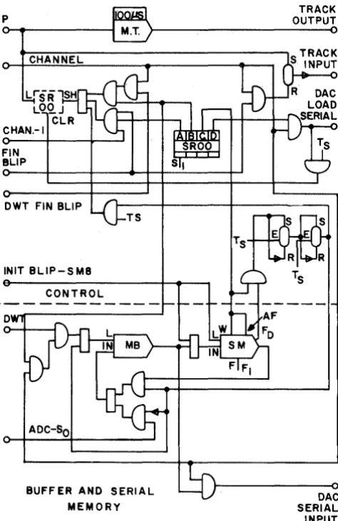
[image:4.613.51.533.49.345.2] [image:4.613.299.539.468.709.2]DESCRIPTION OF TRANSPORT DELAY PROGRAM OPERATION
The HYDAC program for transport delay is divided into three basic sections: 1) The conversion pro-gram which is time-shared by up to 10 channels,
I
2 3
4
OAC 5 LOAD SERtAL 6
7
8 9
10
MPXR
INC
SMa
li
'-as shown in Figure 7a; 2) The Control and Memory program which is duplicated for each channel, as shown in Figure 7b; and 3) The Sampling and Interpolating Program which also is duplicated for each channel, as shown in Figure 7c. Certain portions of this program ••. such as the
SS
I
2
3
1--+---1"""14 1-+--+-1
S
LS
TRAI
TRA2
G D~---..,
C C~--
B -Sj
SOTU
a
OAC'S
I A~---~
2
3
4
5
6.
5
6
7
8 '--+-~19
10
[image:5.612.81.532.138.711.2]p
CHANNEL
CHAN.-I
FIN BLIP
OWT FIN BLIP
INIT BLlP-S Me
o
CONTROL
BUFFER AND SERIAL
MEMORY
TRACK OUTPUT
OAC SERIAL INPUT
FIGURE 7b: Control and Memory Program per channel
Input Sampling and Output Interpolator •.• may be eliminated, depending upon the requirements of the problem. If only a fixed delay is desired, the Sampling Pulse Generator program can be simpli-fied, as well.
Operation of the basic program functions are described briefly in the following sections.
Pulse Generator: Individual channel sampling rate signals are generated from voltage-to-pulse-rate converters that produce sampling signals, P, at rates proportional to their input analog voltages, V. This circuit, shown in Figure 7c, employs a standard analog summing amplifier, an integrator, and a potentiometer set to W TIL. In addition, there is a HYDAC comparator, 2 D-A switches, and a logic differentiator circuit. The comparator output is low (binary 0) until the integrator output ex-ceeds the bias voltage applied to the summer input, at which time it goes high (binary 1). The time required is dependent upon the product of the bias voltage, the pot setting (W TIL), and the magnitude of the analog voltage representing the
Velocity, V. A high signal at the comparator output causes the differentiator to produce an output signal, P, which is high for one clock time and, in addition, switches an opposite polarity bias to the summing amplifier by means of the D-A switch. The polarity of the rate voltage ap-plied to the integrator is also switched. eventually causing its output voltage to be reduced, thus allowing the comparator output to go low, produc-ing a second signal, P, which starts the cycle over.
Multiplexing and Conversion: When the sample rate signal, P, goes high, a flip-flop is set causing the complement of its output to go low. This switches the input track-store amplifier to hold X(t) at the value it had when P went high. When the input multiplexer is stepped to the channel, the ADC converts the sampled voltage to an equi-valent 13-bit binary number (12 bits plus sign). When the conversion is completed, a high signal from the ADC causes a differentiator to produce a high signal for one clock time. This high signal
~-N
.
vs
-x_ttl CJ(MULTIPLEXER TRUNK) TRACKINPUT LOGIC TRUNK INPUT SAMPLING
TRACK OUTPUT
OAC TRUNK
SAMPLING PULSE GENERATOR
OUTPUT INTERPOLATOR
[image:6.615.38.275.59.424.2] [image:6.615.298.537.340.704.2]causes: 1) a flip-flop (FIN*) to be set to produce a high signal on its output; 2) the input multi-plexer to be stepped to the next channel; 3) an indication to be given to the channel "control" circuit that the conversion has been completed; and 4) the input track- store amplifier to be re-turned to the track state by resetting the flip-flop originally set by the sampling rate signal. The high signal on the output of the FIN* flip-flop produces a signal on the output of a second flip-flop which is high for one serial word time. This signal, ANDed with FLG, loads the converted value of the sampled input for the 13- bit data word time (DWT) from the ADC to the Memory Buffer selected by the output multiplexer. After a time interval equal to a serial word time, a finish signal (DWT FIN BLIP) steps the output multi-plexer (shift register) to the next channel prep-aratory to the next conversion, and the DAC counter (GC01) to the next channel. A blocking operation is included if data is being loaded into the DAC. Only one of the shift register stages is active at a time. The active stage selects a memory channel corresponding to the selected input signal, determines which input track- store ampli-fier to return to the track state upon completion of the ADC conversion, and outputs the word two points ahead on the stored function from the serial memory to its memory buffer for transfer into the DAC channel. Each input shift pulse advances the active stage of the register one step. When the last stage is active, the shift signal transfers the active signal around the end, back to the first stage. Note that the multiplexing and conversion program operates independently of the timing of the rest of the program.
Control: The basic control of the program for each channel is performed by a shift register (SROO). The sampling routine is initialized when a high P signal causes the A flip-flop in the register to be set to the ONE state. After a conversion has been completed by the ADC and the output multiplexer has stepped to the channel, the output of an AND gate goes high, advancing the control by shifting the register from the A to the B stage. The output of the flip-flop in this stage goes to the ONE state, allowing the converted sampled value of the input to be loaded from the ADC to the channel memory buffer. After a time interval equal to one word time, the register is shifted from the B stage to the C stage by a high signal on the output of the second AND gate. The C stage flip-flop goes to the ONE state, permitting the word in the memory buffer to be stored in the serial memory, and advances the serial memory "flag" for readout of the next point. When the
j + 2 word has been read from the serial memory
into its memory buffer, the control is advanced to the D stage. When the output multiplexer returns to that Channel, a word time signal is generated to load the memory buffer into the appropriate DAC channel. At the completion of this loading, the control register is cleared. The cycle is then ready to be repeated upon generation of the next sampling rate pulse.
Buffer and Serial Memory: Loading of the memory buffer with the converted sampled value of the input takes place when a high signal appears at the output of the AND gate connected to the LOAD input of the MB. After the word is loaded into the buffer, the control shift register is advanced to the C stage, which causes a high Signal to be applied to the Wand AF terminations of the serial memory. When the word position containing the F1 "flag" is detected, the high W line causes the contents of the memory buffer to be loaded into this location in the serial memory (the func-tion point originally stored in this posifunc-tion has been read out during the Pj -2 pulse). At the same time, the high AF line advances the F1 flag to the next word position to enable the storage of the Pj+ 1 sample. When the word containing the F1 flag is detected, the FLAGGED DATA line goes high, which initiates a logic and timing circuit which effectively counts two word times. After a time interval equal to two word times, the output of a flip-flop goes to the ONE state, allowing the memory buffer to be loaded with the word two pOints ahead on the stored function. This word is then held in the memory buffer until it can be loaded into the DAC channel. This value is then held in the DAC until the Pj+ 1 sampling cycle, when it is used to interpolate the function between pOints j+ 1 and j+ 2. Note that no particular serial memory has been assigned. The choice will de-pend upon the total number of storage points re-quired and the minimum delay. A description of the HYDAC Serial Memory Units, including the minimum time to load a complete function, is presented in Appendix I.
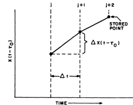
In terpo I ation: Reconstruction of the stored func-tion is performed by a linear interpolafunc-tion cir-cuit. This circuit accepts the sampled data points from the DAC and converts them into a continuous analog function with straight line segments between points. The period between samples is a variable as defined by the following relationships from flow through a pipeline.
TIme e ay · D I
=
T D=
Length of Pipeline L----===----=----
Velocity of Flow - VTD
L
Period between Samples = at = =
-W
Then
As shown in Figure 8, ~X(t - Tn) is the difference between the j + 1 point on the curve held in the
j+1 j+2
I i
~
STORED POINT
0
----j}
6X(t-TO)
...
I
-... I
)(
I I
I I
J.-6t~
I I
I I
I I
TIME
•
FIGURE 8: Linear Interpolation Between Stored Points of Delayed Function
nAC register (loaded into the nAC at the end of the j-1 sample), and the value of the function on the output of the integrator when the register contents are sampled by the track-store ampli-fier. Since W T and L are known constants for a given problem, and V is the analog voltage con-trolling the duration of the delay, the rate of change of the delayed function can be formed by a multiplier and integrated to produce the func-tion. A new value of ~X(t - Tn) is obtained for each sampling pulse. A high signal to the input of a monostable timer produces a high signal which switches the track- store amplifier to the tracking state. This amplifier samples the dif-ference between the voltage output of the nAC and the integrator to form ~X(t - Tn) for the j to j+ 1 interval. At the end of a 100 microsecond delay (sufficient to enable the track- store amplifier to accurately sample the voltages), a low signal switches the track-store amplifier to the hold state, fixing ~X(t - Tn) for the interval. The integrator then integrates the rate as determined by V to produce the function.
Sample Results: A plot of typical results obtained on the HYDAC system using the Transport nelay Program is shown in Figure 9.
8
The input signal, Xl (t), is a sine wave (sin
wt,
with
w
= 1) modulated by a sawtooth wave of lower frequency. The signal x2(t) has the same character as signal xl (t) , except that the frequency of both the sine wave and the sawtooth- wave for the former are ten times higher. For the first channel, a sampling rate, P, of 10 points per second was used, while the second channel employed a sam-pling rate of 100 points per second. SM-8' s were used for this sample program; Tn1 was 25.6 sec-onds and T n2 was 2.56 secsec-onds.To illustrate the effect of variable delay, the velocity of both channels was reduced by a factor of two at the point indicated in Figure 9. Although a pure step change in velocity may not be realiza-ble in physical systems, the simulated condition can be considered a worst case test. Since the fluid is incompressible and no mixing is as-sumed, the step change in input velocity caused an immediate reduction in the frequency at the output of the pipe. This new frequency is sus-tained until the input appears at the output with the new velocity. In Figure 9 it can be seen that channel one had not yet, at the end of the recording shown, reached the new steady state.
CONCLUSIONS
A general purpose HYDAC program for multi-channel variable transport delay has been de-scribed. The major features of this program, in terms of capacity and versatility, include:
• The provision of up to ten independent channels of delay
• The availability of storage capacities of 16, 64 or 256 words per channel
• The capability to obtain a wide range of delay times since each independent channel can accept a different velocity variable
• The extension of this wide-range-delay-time capability since each channel can use a Serial Memory Unit of different capacity
• For example, the capability to provide delay from 25 to 800 milliseconds at 0.5% accuracy for signal frequency of 10 cps
[image:8.620.42.268.171.349.2]This hybrid transport delay simulation program is one of a series of standard geheral purpose programs which are available as "software" for the HYDAC System. Other programs, including
'Ut
F
'-.::C-I
~-J.
...
:rMn, 'se~.
....
l":
":::::
,.-.
' I :
, ~ ,
!
l:
! !
I
....
f·_.. /'::':"-~-C-" ..
. c _
::- co::
, ..
~ ...
fc'
one for multi-tapped transport delay of one func-tion for use in correlafunc-tion analysis, are available or are scheduled for inclusion in the overall HY-DAC "software" capability.
_Ctc-·:·· :-.'::::: I
:.::t:.c::.:
:=
:-::Ce-::::':
._F= >,_::=-
r=:=
:
.. -; viva
"·1--''', '.
.'
··, .... Jz:': ':.: CO'
... /_. /-._._-
._-_ .. -_._-- '-i--_C ' ....
...
.. :
i
'::cc
'\.,
:...
.- --.
; ..
I: :.
=-=
,-Y2
i~;~~~~i~-+-+~"-+---+~~ve/2;
,• i
y-,~ul-t
' t
-. ,- - ·f~::CC:c:.=F.. t·: .:._ ..
•
m" III
i
1111
~
[image:9.612.75.547.117.539.2]-....
FIGURE 9: Sample Results for Two Channel Transport Delay Including ,Effect of Velocity Change REFERENCE
APPENDIX I
-GENERAL DESCRIPTION OF HYDAC SERIAL MEMORY UNITS
The Serial Memory Unit used to store X(t) in the transport delay program can be described as a device for storing a table of numbers, or digital "words", that represent a sequence of sampled values of an analog signal. All numbers are stored as serial binary words of 16 bits each. Each unit has its own control Circuitry for writing, ad-dressing, and reading the tabular values in the proper sequence. The three sizes of Serial Memory Units are the SM-8 with a capacity of 256 words, the SM-6 with 64 words, and the SM-4 with 16 words. Each size of memory unit has a different Read/Write Cycle rate. This rate is the maxi-mum number of data words per second that, in the normal mode of operation, can be written into and read from memory in sequence. Any lower rate can be used, as may be required by the analog sampling rate. The entire stored table of num-bers can be read rapidly from memory in a single Read/Write cycle but, in normal use, a single word is selected from the table and a new word written into the table in the same position during a cycle. The selected position is then moved to the next in the sequence.
The tables of data words are addressed by a moving index "flag". The flag is moved forward one step each Read/Write Cycle during which the AF (Advance Flag) control line is energized. The flag may be moved in the reverse direction, one step per cycle, by the RF (Reverse Flag) control line. If the AF line is energized all the time, the entire table will be addressed at the full Read/Write cycle rate (512 cps, 2048 cps, or 8192 cps), and thus the flag will sweep the entire func-tion table in the minimum sweep time (0.5 sec-onds, 31 millisecsec-onds, 2 milliseconds). If the flag is moved beyond the last word position in the sequence, it steps to the first position.
10
The tabular data words selected by the moving flag are "read out" by forming the logical product (with an AND gate) of the data output and the FD control line. The FD (Flagged Data) line provides an enabling signal long enough to pass the serial bits of the indexed or flagged word, one each Read/Write cycle. Thus, reading from the memory is possible without employing any specific "read" control Signal.
New data is written into the memory at the flagged position whenever the W control line is energized and the new serial data is available at the input.
The F (Flag) control line permits the simultaneous use of as many as three independent flags in the Serial Memory Unit. Thus, in special programs, it is possible to move these flags back and forth independently to select the desired position for reading or writing. The L (Load) control line is similar in function to the W line but is used to pre-store or initialize the memory unit with special data, such as initial flag locations.
The range of memory sizes and maximum Read/ Write cycle rates satisfies a wide range of prob-lem requirements. For transport delay programs, the required minimum sampling rate and the delay time determine the choice of memory unit. For function storage and generation, the SM-8 unit will handle a 256-point function in as short a period as 0.5 seconds. Thus, for real time programs the SM;....8 is very satisfactory; however, for high speed repetitive programs the SM-6 is better, since it can be used with a time base as short as 31 milliseconds. The SM-4 is useful mostly for very short delays and with other units. It must be noted that function tables of any size can be program-med simply by cascading Serial Memory Units.
APPENDIX II
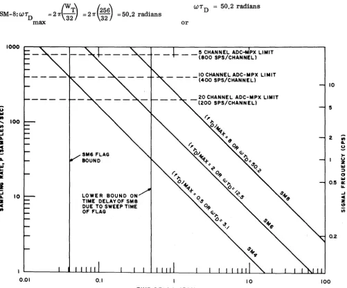
-To apply a figure .of merit to different methods of simulating transport delay, the product of the frequency and the time delay for a particular accuracy is generally used. This product
-WTD - represents the storage capacity of the time delay, or the phase shift in radians which one can obtain with a particular transport delay system. The fourth-order polynomial approxima-tion provides approximately 7.5 radians of delay with a one-degree phase error which corresponds to approximately 0.5% error in amplitude. To obtain the same accuracy with the serial memories in this HYDAC program, 32 pOints per cycle must be stored using linear interpolation of the output function. Therefore, one can establish a maximum
W T D product for each serial memory unit.
SM-8:WT
n
=21TG'-:)
=2,,(;~6)
=50.2
radians max-
UIII
.,.
1000
'- 100
fit
&II
-'
0-a
c
.,.
-I
:;
A. 10
a
c
.,.
I
0.01
SM6 FLAG BOUND
LOWER BOUND ON TIME DELAYOF SMS DUE TO SWEEP TIME OF f"LAG
0.1
SM-6:WT
n
=2k;:)
=2,,(::) =12.5
radians maxSM-4:WT
n
=2~:) =2"(!~)
= 3.1
radians maxBy this criterion, it is obvious that the SM-8 is the most powerful unit. However, the larger storage unit is most useful only for the longer delay times, Le. those exceeding 0.5 second (there is no inherent upper limit to the delay).
If the minimum delay time is 0.5 second, the maximum analog frequency.for this unit, at 0.5% preCision, is:
WT D
=
50.2 radiansor
_ _ 5 CHANNEL ADC~jPX LIMIT (SOO SPS/CHANNEL)
10 CHANNEL ADC-MPX LIMIT - - - - (4·00 SPS/CHANNEL)
20 CHANNEL ADC-MPX LIMIT (200 SPS/CHANNEL)
10
~ u
z
....
::;)
o
'"
0.5 a::
0.2
100
IA.
-'
C
Z
"
en
TIME DELAY, SECONDS
[image:11.618.65.566.287.703.2]f = 50.2 104
max 211" T D 6.28 16.6 cycles/sec
For shorter delays and higher frequencies, the SM-6 unit provides a minimum delay of 0.031 seconds. In this case, the maximum analog fre-quency is:
f = 12.5 = 64 cycles/sec max 27T T D
The corresponding frequency for the SM-4 is approximately 256 cps.
The following equation relates sampling rate, P, to time delay, TD:
W
T
P = - - CW = number of words in SM unit)
TD
T
Taking the log of both sides
log P = log W T - log T D
Figure 10 shows this relationship as a straight line on log-log paper. Also included in this graph are the conversion rate limits and the sampling rates required to provide 32 points per cycle for various analog input frequencies. This graph permits the programmer to determine rapidly what Serial Memory Unit to use for a particular application and the allowable analog frequency.
To illustrate the use of the chart, the sample requirement described under Program Capabili-ties will be used. With a signal frequency, f, of 10 and a TDmax of 0.7 second, the fTDmax is 7, which is below the SM-8 and above the SM-6 indicating that the SM-8 unit must be used. Enter-ing the chart on the 0.7- second delay line, a sampling rate, P, of approximately 370 points per second is found for the 8M-8, which is well below the five-channel ADC-MPX limit. Since this point is over the f=10 cps line, an accuracy somewhat greater than 0.5% will be obtained. Thus, the chart permits the programmer to compare conveniently the requirements of the problem with the capabilities of the program, to determine the size of memory required and whether time-scaling of the analog is indicated to fulfill the require-ment.
APPENDIX III
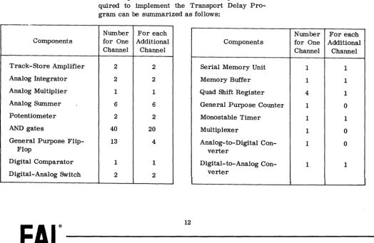
-
r-.----Components
Track-Store Amplifier
Analog Integrator
Analog Multiplier
Analog Summer
Potentiometer
AND gates
General Purpose Flip-Flop
Digital Comparator
Digital-Analog Switch
The complement of HYDAC 2000 components re-quired to implement the Transport Delay Pro-gram can be summarized as follows:
Number For each
for One Additional Components
Channel Channel
2 2 Serial Memory Unit
2 2 Memory Buffer
1 1 Quad . Shift Register
6 6 General Purpose Counter
2 2 Mon6stable Timer
40 20 Multiplexer
13 4 Analog-to-Digital
Con-verter
1 1 Digital-to-Analog
Con-2 2 verter
12
EAI
®ELECTRONIC ASSOCIATES, INC. Long Branch, New Jersey
Number For each for One Additional Channel Channel
1 1
1 1
4 1
1 0
1 1
1 0
I 0
I 1
ADVANCED SYSTEMS ANALYSIS AND COMPUTATION SERVICES/ANALOG COMPUTERS/HYBRID ANALOG-DIGITAL COMPUTATION EQUIPMENT/SIMULATION SYSTEMS/
[image:12.618.31.555.401.742.2]