Abstract—
One of the concerns to put on the
energy efficiency is in relation to the system
power factor. From the view of industrial
practices, low power factor might cause
equipment failure and higher operation costs. This
paper proposes a conceptual design of
microcontroller-based self-adaptive power factor
corrector (PFC) circuit with the intention to be
used in the poor power factor (either linear or
nonlinear) loads applications. The design of this
auto-adjustable power factor corrector is to ensure
the entire power system always preserving almost
unity power factor and thus optimizing the current
consumption. Power factor value is initially
measured via microcontroller and it is then
compared with a pre-determined reference value.
The poor power factor of the entire system will
then be adjusted by the aid of the microcontroller
to as close as the pre-determined value as
possible. The proposed power factor corrector has
an adjustable sensitivity of 50 microseconds or 0.9
degree interval step setting. The conceptual design
of the power factor corrector circuit has gone
through a set of simulation tests using Computer
Aided Engineering (CAE) tool. The results
obtained are verified that the proposed PFC circuit
is capable to produce a reliable output and can be
further implemented in practical applications.
Keywords: Energy saving, Microcontroller, Power factor corrector.
This work was supported in part by Research Management and Innovation Centre, Universiti Tun Hussein Onn Malaysia under the research vote number 0302.
B.C. Kok is with the Department of Electrical Power Engineering, Faculty of Electrical and Electronic Engineering, Universiti Tun Hussein Onn Malaysia, Parit Raja, Batu Pahat, Johor. (phone: 4537548; fax: 07-4536060; e-mail: [email protected]).
C. Uttraphan is with the Department of Computer Engineering, Faculty of Electrical and Electronic Engineering, Universiti Tun Hussein Onn Malaysia, Parit Raja, Batu Pahat, Johor. (e-mail: [email protected]).
H.H. Goh is with the Department of Electrical Power Engineering, Faculty of Electrical and Electronic Engineering, Universiti Tun Hussein Onn Malaysia, Parit Raja, Batu Pahat, Johor. (e-mail: [email protected]).
I. INTRODUCTION
OW power factor in the power distribution system causes the energy crisis in the supply of energy resources.Most of industrial electric loads have a low power factor not exceeding 0.8 and thus contributes to the distribution system losses [1-4]. There are different methods of power factor correction implemented with large lagging or leading nonlinear loads [l]. One of the new approaches is to use a variable inductor in parallel with a fixed capacitor as a reactive power compensating circuit [5-6]. The inductor current is controlled by adjusting the firing angle of two anti-parallel connected thyristors or using TRIAC [4]. The adjustment of the thyristors' firing angle is made in accordance to the result of a comparison between the measured value of a certain system parameter with its reference value [7-10]. This approach is more reliable because it involves the counts of the leading and lagging current in the power factor with a very accurate and precise step setting, in terms of calculating the phase angle, in the power factor corrector. In spite of giving pre-calculated relations between the system power factor and the static VAR compensator firing angle, the suggested power-factor correction scheme do not give a real-time solution to the problem of low power factor in nonlinear loads.
This paper proposes a real-time microcontroller-based power factor correction scheme for low power factor loads. The software and hardware required to implement the suggested adaptive power factor correction scheme are explained, and its operation is described.
II. BLOCKDIAGRAMSANDDESCRIPTIONS
The block diagram of the microcontroller based power factor corrector is shown in Figure 1.
A microcontroller of PIC16F84A with a crystal of 4 MHz has been utilised in the proposed scheme. The static compensator employed in the system is a parallel combination of a fixed capacitor C and a TRIAC controlled reactor (inductor L). A small inductance L1is connected in
series with C to prevent parallel resonance.
Two back-to-back thyristors are used to control the current flow through the reactor. The supplied voltage and current signals, taken through a potential transformer and a current transformer, respectively, are applied to band pass filters (BPF 1 and BPF 2). The detail of the filter design is depicted in Figure 2. The outputs of these two filters are the fundamental complex waveforms of the supplied voltage
A Conceptual Design of Microcontroller-Based Power Factor Corrector Circuit
B.C. Kok, C. Uttraphan, and H.H. Goh
L
Proceedings of MUCEET2009 Malaysian Technical Universities Conference on Engineering and Technology June 20-22, 2009, MS Garden, Kuantan, Pahang, Malaysia
[image:2.595.344.509.49.316.2]
and current, respectively. Subsequently, the two sinusoidal waveforms are being changed to square waves through two zero-crossing detectors (ZCD 1 and ZCD 2) as the microcontroller can only detect the digital signal input, or known as ‘pulse’. Figure 3 shows the particular system voltage and current waveforms.
[image:2.595.52.296.136.301.2]Figure 1: Overview of the block diagram for the microcontroller-based power factor corrector.
Figure 2: Bandpass filter.
Figure 3: System current and voltage waveforms for (a) leading power factor, and (b) lagging power factor.
[image:2.595.66.272.348.528.2]The synchronizing circuit shown in Figure 4 produces a pulse at each zero-crossing of the supplied sine wave voltage. The rising edge of the synchronizing circuit output pulse is synchronized with the zero-crossing of the input sine wave voltage. The output pulses obtained from the synchronizing circuit are then applied to the input of microcontroller as a reference in order to trigger the TRIAC firing angle which is to make sure the pulse is synchronised to the input sine wave voltage.
Figure 4: Synchronizing circuit.
Afterwards, the pulse signal from the microcontroller drives the gates of the two back-to-back thyristors or TRIAC so as to control the reactor current. The phase angle, φm between the fundamental components of the supplied voltage and current (V and I respectively) is measured by the microcontroller. The details of the source code developed to achieve the above task are explained in the next section. The measured phase angle φm is then compared with a reference value, φrthat gives the required power factor (displacement factor). The resultant error signal is used to adjust the number that is loaded into the programmable interval timer in order to change the firing angle, α of the thyristors in the
b) Lagging power factor V2
I’s Is
V’s Vs
t
t
t
t
t
a) Leading power factor I’s
Is
V’s Vs
V2
t
t
t
t
t iS
L
TRIAC Potential
Transformer
Variable
Non-Linear
Load AC Supply
Voltage 240v 50Hz
Current Transformer
L C
L1
N
i1 i2 i3
V2
I’S V’S
VS
Opto-isolator TRIAC Driver Synchronizing
circuit
BPF 1
BPF 2
ZCD 2 ZCD
1
[image:2.595.306.548.501.592.2]
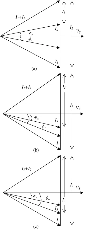
static compensator circuit. These changes should be in the direction that reduces the difference between φm and φr to a certain acceptable tolerance value. Figure 5 shows the phasor diagrams of the system currents shown in Figure 1. These phasor diagrams may help to explain the operation principle of the proposed adaptive power factor corrector and to distinguish between the following three cases, assuming φr is always lagging:
(1)φr and φm have different signs.
[image:3.595.80.259.227.709.2](2) φr and φm have the same sign and |φr| > |φm|. (3) φr and φm have the same sign and |φr| < |φm|.
Figure 5: Phasor diagram of the system currents: (a) φr and m
φ have different signs; (b) φr and φm have the same sign and |φr| > |φm| ; (c) φr and φm have the same sign and |φr| < |φm|.
In cases (1) and (2), the reactor (inductor L) current must be increased, and consequently, α must be decreased to get the required power factor (φm=φr). In case (3), the reactor current must be decreased, and consequently, α must be increased to have φm=φr. The above mentioned cases are taken into consideration in the main control program. In the proposed scheme, the system power factor is improved by adjusting the displacement factor only. The distortion factor may be improved by using filters adjusted to remove the dominating harmonics.
III. MICROCONTROLLERROUTINES
The microcontroller PIC16F84A has two I/O ports, namely PORTA and PORTB. PORTB has eight pins. RB0, RB1 and RB2 are programmed to operate as input pins, in which the RB1 representing voltage, RB2 representing current and RB0 representing synchronizing pulse. Meanwhile, the pin RB3 operates as output pin.
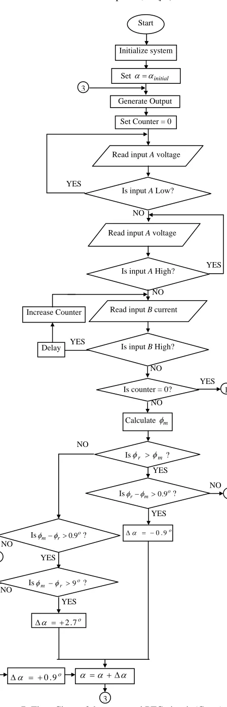
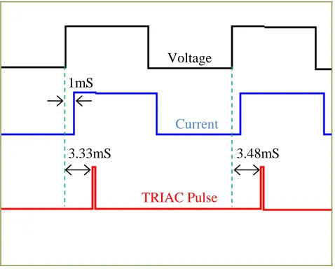
[image:3.595.312.543.397.495.2]In the first stage, the system is initialized, and the TRIAC triggering angle, α is set to the chosen initial value, αinitial. The value of α is loaded into one general purpose file register in the microcontroller, named as rALPHA. The initial triggering signals (60 degree or 3.33mS) are shown in Figure 6. The flow chart of the program has been developed and is given in Figure 7.
Figure 6: The initial triggering signals from PIC. The Counter register function is to count the number of the steps which is lagging or leading of the current (RB2) for determining the phase angle φm. A low input test followed by a high input one is first performed on input RB1, which represents the main value of the complex supplied voltage waveform. This is to ensure that φm, is measured accurately irrespective of instant switching of the system.
When input RB1 goes low at the end of the high input test, the microcontroller starts reading and testing input RB2. If the input is high, this denotes that the main supplied current lags the main supplied voltage and that can be referred to the case of φr >φm or the φr <φm whereφr is the reference value. As long as input RB2 is high, the microcontroller keeps looping and testing the input.
The Counter is incremented after each test. The loop time, D (µs) may be adjusted to any suitable value by adding the required delay time, since there is a delay time in looping period. When the input RB2 goes low, the contents of Counter are tested. If the content of Counter is not equal to 0, the main supplied current is lagging the main supplied
180° 360°
60°
t V
5V
60° I1
IS
I1+I2
(a) r
φφm
I2
VS
I3
I1 r
φ I1+I2
m
φ
IS
VS
I2
(b)
I3
I1
VS
IS m
φ
r
φ I1+I2
I3
(c)
voltage by an angle, φm which equals to the multiplication
[image:4.595.304.544.50.425.2] [image:4.595.55.279.77.773.2]of Counter’s content to the loop time, D (µs).
Figure 7: Flow Chart of the proposed PFC circuit (Cont.)
(Cont.) Figure 7: Flow Chart of the proposed PFC circuit. The microcontroller will then distinguishes whether it is the case of φr >φm or the case of φr <φm and thus compares the measured phase angle φm with the required or
reference value φr, and chooses the change, ∆α in the
TRIAC firing angle, α accordingly, as shown in Figure 7. After that, the microcontroller jumps back to reload the rALPHA with the new value of α and then tests RB1 after clearing the Counter, and the above sequence is repeated. If the contents of Counter are found to be zero, this means that input RB1 is low throughout the test, which in turn means that it is in case 1 in which the fundamental supplied current is leading the fundamental supplied voltage (see Figure 3). In such a case, the microcontroller branches (Figure 6) read and test the input RB2.
As long as the RB2 is low, the microcontroller continues looping and testing that pin. When RB2 goes high, pin RB1 is read and tested. As long as RB1 remains low, the microcontroller will continue looping and testing RB1. Register Counter is incremented after each test. If the contents of Counter are found to be zero, this means that φm
equals to 0, which in turn means that the fundamental supplied voltage and current are in phase. In such a case, the value of α is kept constant, and the microcontroller jumps back to reload the rALPHA withα , and a new cycle of the testing procedure is started.
NO Read input B current
Is input
BLow? 1
NO
Calculate φm
Is input A
Low? Read input A voltage Increase Counter
Delay
YES
YES
YES YES
NO
3 Is Counter
= 0?
Is
o m r+φ >9
φ ?
3
o
9 . 0
− =
∆α
α α α= +∆
o
7 . 2
− = ∆α
NO
NO
NO
Is o
r m−φ >0.9
φ ? ∆α = −0.9o
YES
NO YES
3 Isφ >r φm?
Is o
m r−φ >0.9
φ ?
α α α = +∆ YES
YES
NO Is
o r m −φ >9
φ ?
o
7 . 2
+ = ∆α
o
9 . 0
+ = ∆α
YES Is counter = 0?
Calculate φm
1 Start
Initialize system
Set α =αinitial
Generate Output 3
Set Counter = 0
Read input A voltage
Is input A Low?
YES NO
Is input A High? Read input A voltage
NO
N Is input B High? Read input B current Increase Counter
Delay YES
YES
NO
NO
3
If the contents of Counter are not zero, the program starts calculating φm. In this case, φr and φm have different signs
(since φr is always lagging), and hence, the value φr+φm
is tested to find the actual deviation of φm from φr. A large
deviation needs a large step change ∆α in the thyristor firing angle α , whereas a small deviation needs a smaller∆α. After the rALPHA is reloaded with the new value ofα , the microcontroller jumps back to read and test pin RB1 after clearing the Counter, and the above sequence is repeated.
Referring to the calculated values, all actual measurements and comparison of φm and φr are made in
microseconds rather than in degrees. The loop time, D is adjusted to be 50 µs, which corresponds to an angle of 0.9o at a supplied frequency of 50Hz. Since the LSB in Counter represents a delay angle of 0.9o, a change (∆α) of 0.9o corresponds to a change of a decimal number of 1, whereas a change of ∆α equals to 2.7o corresponds to a decimal number of 3. When the differences between φmand φr is
decreased to a value less than or equal to 0.9o, φmis
considered to be equal to φrand thus α is no longer
changed. However, one may change this difference to any other value that achieves the required accuracy.
IV. SIMULATIONRESULTS
The proposed power factor corrector circuit is tested using Proteus Design Suite in which the simulations have been divided into 5 study cases depending on the loading conditions, i.e.: (1) purely resistive load, (2) large inductive load (with φm - φr > 9°), (3) small inductive load (with φm -
φr < 9°), (4) inductive load with over corrected condition
(with φr > φm and φr - φm > 0.9°), and (5) capacitive load
(with φr + φm > 9°). For all study cases, the reference phase
angle, φr is set to 6 steps (5.4°) or the system’s power factor
will be corrected to 0.9956. Study Case (1)
In this case, the system voltage and current waveforms are always in-phase. The microcontroller does not correct the TRIAC firing angle (φm < φr) as depicted in Figure 8.
Figure 8: Waveforms for study case (1).
The TRIAC firing angle is initially set to 60° or equals to 3.33mS. Since the voltage and current waveforms are operating at the same phase all the time, the firing angle is consequently remains at its initial setting angle for each cycle (1 cycle = 20mS for 50Hz supply).
Study Case (2)
The power system is connected to large inductive load so as the system current lags the voltage by 1mS (18°). In this case, the calculated φm is 20 steps. Since φm - φr > 9°, the
firing angle must be increase +2.7° (150µS) in the next cycles so as to decrease the reactor current.
[image:5.595.308.547.238.430.2]Obviously, the firing angle before the correction is 60° (3.33mS) and the firing angle after the correction is 62.7° (3.48mS) as shown in Figure 9.
Figure 9: Waveforms for study case (2). Study Case (3)
The power system is connected to small inductive load with the system current lags the voltage by 500µS (9°) and thus φm is calculated as 10 steps. Since φm - φr < 9°, the
firing angle must be increase +0.9° (50µS) in the next cycles until φm = φr.
[image:5.595.52.549.580.777.2]This scenario is depicted in Figure 10. The firing angle before the correction is 3.33mS and after the correction, it is adjusted to 3.38mS (60.9°).
Figure 10: Waveforms for study case (3). Voltage
Current
TRIAC Pulse
3.33mS
Voltage
Current
TRIAC Pulse
3.48mS 3.33mS
1mS
Voltage
Current
TRIAC Pulse
3.38mS 3.33mS
Study Case (4)
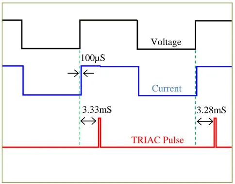
This study case representing the scenario of the over corrected as in case (2) and case (3). As shown in Figure 11, the firing angle is now over corrected to the condition that φr
> φm and φr - φm > 0.9°. The system current at this moment is
[image:6.595.48.290.142.332.2]still lagging the voltage by 100µS. Thus, the firing angle now has to be decreased by -0.9° to 3.28mS (59.1°).
Figure 11: Waveforms for study case (4). Study Case (5)
The power system is connected to capacitive load and the system current leads the voltage by 2mS or 36°. In this case, the phase angle (φm) is calculated as 40 steps. According to
the phasor diagram in Figure 5(a) and the flow chart in Figure 7, if φr + φm > 9°, the firing angle must be decreased
[image:6.595.54.558.440.663.2]by the steps of -2.7° (-150µS). This event can be observed in Figure 12, in which the corrected firing angle is 3.18mS (or 57.3°).
Figure 12: Waveforms for study case (5).
V. CONCLUSION
A microcontroller-based power factor corrector for single-phase low power factor loads has been presented in terms of the software algorithm development. The system can adjust the supplied system power factor to almost any required reference value. The proposed power factor correction scheme is designed to operate with most of the possible lagging or leading values of the load power factor. This shows the adaptability of this power factor corrector. The system design allows more accurate in the measuring and compensating power factors than the passive power factor designs. This is because its operation principles’ is based on the measurement of the displacement angle between the fundamental components of the supplied voltage and current, rather than measuring the system voltage signal. The principle of operation adopted in this paper may be applied further in designing the power factor correction schemes for loads driven by 3-phase voltage supplies.
ACKNOWLEDGMENT
The authors gratefully acknowledge the Research Management and Innovation Centre, Universiti Tun Hussein Onn Malaysia (UTHM) by funding this research under the research vote number 0302. The authors would also like to express greatest thankfulness to the staffs in the Laboratory of Electric Machines and Drives as well as the Laboratory of Electric Power, UTHM for their valuable contributions towards the success of this research.
REFERENCES
[1] Alexander, C.K. and Sadiku, M.N.O. (2000). “Fundamentals of Electric Circuit” United States of America: McGraw-Hill Companies, Inc.
[2] Stephen, J. C. (1999). “Electric Machinery and Power System Fundamentals.” 3rd.ed. United State of America: McGraw-Hill Companies, Inc.
[3] John J. Grainger, William D. Stevenson (1994). “Power System Analysis.” New York: McGraw-Hill.
[4] Jos Arrillaga, Neville R. Watson (2003). “Power System Harmonics” 2nd.ed. Chichester: John Wiley.
[5] J. E. Miller (1982). “Reactive Power Control in Electric System.” New York: Wiley
[6] Roger C. Dugan, Mark F. McGranaghan, H. Wayne Beaty (1996). “Electrical Power Systems Quality” 1st.ed. New York: McGraw Hill. [7] Paul Gill (1998). “Electrical Power Equipment Maintenance and
Testing.” Boca Raton, FL: CRC Press.
[8] Keith Harker (1998). “Power System Commissioning and
Maintenance practice.” London: Institution of Electrical Engineers. [9] Ramasamy Natarajan (2005). “Power System Capacitors.” Boca
Raton, FL: Taylor & Francis.
[10] H.M. El-Bolok, M.E. Masoud, And M.M. Mahmoud (1990). “A
Microprocessor –Based Adaptive Power Factor Corrector for Nonlinear Loads” Faculty of Engineering and Technology, University of Helwan, Cairo, Egypt.
Voltage
Current
TRIAC Pulse
3.33mS 100µS
3.28mS
Voltage
Current
TRIAC Pulse
3.33mS 2mS
[image:6.595.53.302.470.657.2]