International Journal of Emerging Technology and Advanced Engineering
Website: www.ijetae.com (ISSN 2250-2459,ISO 9001:2008 Certified Journal, Volume 5, Issue 3, March 2015)
270
Design and Synthesis of Radix-4 Booth Multiplier Using GDI
Technique
K Siva Sankar
1, K Suganthi
2 1Department of Electronics and Communication Engineering, SRM University, India
2Asst. Prof, Department of Electronics and Communication Engineering, SRM University, India
Abstract—This paper presents a design of low power, area efficient radix 4 booth multiplier using gated diffusion input(GDI) technique and modified gated diffusion input technique. MGDI and GDI plays an important role in design of low power and area efficient circuits. This has led many researchers to take GDI and MGDI technique very seriously in building important circuits related to advanced low power and area efficient CMOS design. The entire design has been performed by using backend tools it has found that there is a consider- able amount of reduction in Average Power consumption (Pavg), delay time. In addition to this there is a significant reduction in transistor count compared to conventional CMOS technique. The simulation of the proposed design has been carried out in H- SPICE tool.
Keywords--Gate diffusion input (GDI), complementary metal oxide semiconductor (CMOS), Booth multiplier, leakage current
I. INTRODUCNTION
A. Background and Motivation
In today‘s electronics world processors became very important for performing multiple operations. Processors consist of adders, subtractions, multipliers etc these consume power, area and also cause delay in data transition. To reduce these parameters we introduce a new arithmetic device called gated diffusion input (GDI) technique radix- 4 booth multiplier [1] which reduces power consumption and also reduces the area.
In past technology, the main concentrations of the VLSI designer were performance of the device, area required, cost and reliability of the complete system. Power dissipation was secondary issue. But in today‘s technology, it has been changed and power dissipation is given equal weight age to area and speed considerations. So many factors have been contributed to this trend. But the main driving factor is the remarkable success and growth of personal computing devices Such as multimedia products, portable desktops and wireless communication systems like personal communicators which need high- speed computation and complex functionality with low power consumption. In such applications, low power consumption is a critical design issue.
Power dissipation in CMOS circuits is caused by three main sources: 1) the charging and discharging of capacitive loads due to change in input logic levels. 2) the short-circuit current arises because of the direct current path between the supply rails during output transitions and 3) the leakage current which is determined by the fabrication technology, consist reverse bias current in the parasitic diodes formed between source and drain diffusions and the bulk region in a transistor as well as the sub threshold current that arises from the inversion charge that exists at the gate voltages below the threshold voltage, The short- circuit and leakage currents in CMOS circuits can be made small with proper device and circuit design techniques. The dominant source of power consumption is the charging- discharging of the node capacitances and it can be minimizing by reducing switching activity of transistors. Switching activity of the digital circuits is also a function of the logic style used to implement the circuit.
II.GDIINTRODUCTION
A. Origin of GDI
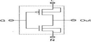
First the GDI basic cell was introduced by Arkadiy Morgenshtein in 2002[4] . The basic GDI cell contains one nMOS and one pMOS transistors with four terminals: G, P, N and D. Input G is the common gate input of nMOS and pMOS transistors, input P is the outer diffusion node of pMOS transistor, input N is the outer diffusion node of MOS transistor, and output D is the common output diffusion node of both transistors. The GDI primitive cells are designed in twin-well CMOS or silicon on insulator (SOI) technologies. The following figure shows the basic GDI cell.
[image:1.612.369.517.619.687.2]International Journal of Emerging Technology and Advanced Engineering
Website: www.ijetae.com (ISSN 2250-2459,ISO 9001:2008 Certified Journal, Volume 5, Issue 3, March 2015)
271
B. Introduction to GDI
Gate Diffusion Input (GDI) method is based on the utilization of a simple cell as shown in Fig. 3.1 which can be used for low power digital circuits . This technique is implemented in twin-well CMOS or Silicon on Insulator (SOI) technologies. In this process, the bulks of both NMOS and PMOS transistors are hardwired to their diffusions to reduce the bulk effect that is dependence of threshold voltage on source-to-bulk voltage . The dependence of transistor threshold voltage on source-to-bulk voltage is as follows
th th (√| F B|√| F|)
Where VSB is source-body voltage, Vth0 is threshold voltage at B , is linearized body coefficient, ΦF is the Fermi potential and η is Drain Induced Barrier Lowering (DIBL) coefficient. Using this procedure power consumption can be reduced along with delay time thereby delivering a reduced power delay product. Consequently area of the circuit is minimized. This analysis is based on the Shockley model in which the drain current ID is represented as shown below
( )
( )
*( )
( )
( )
( )
Where K denotes device transconductance parameter, VTH denotes threshold voltage, W denotes channel width and L denotes channel length.
C. Transient response of GDI cell
The following figure shows the transient response of a GDI cell which is quite similar to that of a standard CMOS inverter
D. Various operations on GDI cell
[image:2.612.365.512.376.530.2]The following table shows different operations of GDI cell
Table I:
Different Operations Of Basic Gdi Cell
N P G OUT Operation
‗0‘ B A ÃB F1
B ‗1‘ A Ã+B F2
‗1‘ B A A+B OR
B ‗0‘ A AB AND
C B A ÃB+AC MUX
‗0‘ ‗1‘ A Ã NOT
III. BASIC GDILOGIC GATES
A. GDI AND gate
The following figure shows the circuit diagram for GDI AND gate
Fig 2: GDI AND cell
The above figure shows the design of an AND gate based on GDI method. It requires a single GDI cell in which the source of the PMO that is port ‗P‘ is connected to GND and ‗A‘ is given as an input to port ‗G‘ while port ‗N‘ is supplied input B.
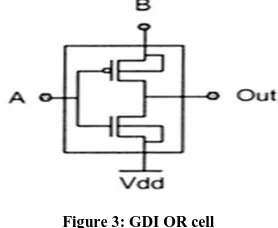
B. GDI OR gate
[image:2.612.56.284.621.709.2]International Journal of Emerging Technology and Advanced Engineering
Website: www.ijetae.com (ISSN 2250-2459,ISO 9001:2008 Certified Journal, Volume 5, Issue 3, March 2015)
[image:3.612.99.238.138.252.2]272
Figure 3: GDI OR cell
The above figure shows the design of OR gate GDI cell in which it consists of a single GDI cell where port ‗P‘ is given an input B, port ‗ G‘ an input ‗A‘ while port ‗N‘ is supplied with Vdd.
C. GDI XOR gate
The following figure shows GDI XOR gate
Fig 4: GDI XOR cell
The above figure shows the design of a XOR gate based on GDI procedure. It contains two GDI cells in which the first cell acts as a basic inverter while for the second cell ‗B‘ is given as an input to port P of the GDI cell whereas ‗A‘ is given as an input to port G and the output of the first cell is given as an input to port N of the second cell.
IV. RADIX-4BOOTH MULTIPLIER
A. Introduction
Multiplier is one of the mostly used building blocks in the digital devices. The high performance DSP systems depend on hardware multiplication to achieve high data throughput. Digital multiplication is a series of bit shift and bit additions, where two binary numbers, the multiplier and the multiplicand are combined into the result.
The entire process consists of three steps: 1) partial product generation, 2) partial product reduction and 3) final addition. There are different types of multipliers available depending upon the application in which they are used.
Basically Multiplier design consists of three operational steps: 1) encode the multiplier bit Y using Booth encoded algorithm and a partial product is produced from the multiplicand X and the encoded multiplier Y. 2) the adder array or partial product compression is used to add all partial products and then reduce them into the form of sum and carry. 3) The final addition using CSA adder or RCA adder in which the final multiplication result is generated by adding the sum and the carry. So, the important blocks in booth multipliers are decoder, partial product generator and adder to generate final result.
B.Radix-4 Encoder block diagram
[image:3.612.51.286.335.475.2]The following figure shows radix-4 encoder block
Fig 5: Radix-4 encoder
Radix-4 multiplication obtains an improvement in the multiplication algorithm due to the less number of partial products entering the Wallace tree to be reduced [7]. This can be achieved by the application of the multiplier recoding, changing from a ‟s complement format to a signed-digit representation from the set {0, ±1, ±2}
Now let us assume that we are giving a triplet of multiplier one at a time in the form of Yi-1, Yi, Yi+1 and gets the encoded output in the form of Neg, X1_b, X2_b, Z. In which X2_b means that the multiplicand is not to be doubled, X1_b means multiplicand is to be doubled and Neg means neither to be doubled nor to be inverted.
C. Partial product generator block diagram
[image:3.612.326.575.349.482.2]International Journal of Emerging Technology and Advanced Engineering
Website: www.ijetae.com (ISSN 2250-2459,ISO 9001:2008 Certified Journal, Volume 5, Issue 3, March 2015)
[image:4.612.324.575.121.352.2]273
Fig 6: Partial product generator
In this block, multiplier bits encoded from the encoder and the multiplicand bits get multiplied and the partial products are generated. Fig. 6 shows the block diagram of 1-bit partial product generator block where the input X1_b, X2_b, Neg, Z are the encoded multiplier bits from the encoder and Xj and Xj-1 are the multiplicand bits which are to be multiplied by the multiplier bits coming from the encoder.
V. SIMULATION RESULTS
[image:4.612.56.291.140.365.2]A. H-spice simulation results for CMOS & GDI AND gates
[image:4.612.324.578.373.591.2]Fig 7: simulation waveform for CMOS AND gate
Fig 8: simulation waveform for GDI AND gate
B. H-spice simulation results for CMOS & GDI OR gates
[image:4.612.50.298.499.711.2]International Journal of Emerging Technology and Advanced Engineering
Website: www.ijetae.com (ISSN 2250-2459,ISO 9001:2008 Certified Journal, Volume 5, Issue 3, March 2015)
[image:5.612.323.582.112.356.2]274
Fig 10: simulation waveform for GDI OR gate
[image:5.612.53.303.132.374.2]C. H-spice simulation results for CMOS & GDI XOR gates
Fig 11: simulation waveform for CMOS XOR gate
[image:5.612.51.295.393.656.2]International Journal of Emerging Technology and Advanced Engineering
Website: www.ijetae.com (ISSN 2250-2459,ISO 9001:2008 Certified Journal, Volume 5, Issue 3, March 2015)
275
[image:6.612.43.579.93.560.2]Fig 13: Input waveforms for booth multiplier 2) output waveform for Booth multiplier:
Fig 14: Output waveforms for GDI Radix-4 booth multiplier
[image:6.612.51.308.132.337.2]VI. PARAMETERS COMPARISON
Table II Parameter Comparison
Gate type CMOS AND
GDI AND
CMOS OR
GDI OR
CMOS XOR
GDI XOR
Delay 46.30
Pico sec
3.73 Pico Sec
40.17 nsec
40 nsec
9.84 nsec
9.8 nsec
Power 20.6
µw
13.43 µw
6.69 µw
0.46 µw
23.1 mw
20.1 mw Transistor
count
6 2 6 2 12 4
International Journal of Emerging Technology and Advanced Engineering
Website: www.ijetae.com (ISSN 2250-2459,ISO 9001:2008 Certified Journal, Volume 5, Issue 3, March 2015)
276
VII. CONCLUSION
This project presents a detailed study of GDI technique and implementation of logic gates and architecture of Radix-4 Booth multiplier using GDI technique The simulation results reveals that there is a considerable reduction in power when compared with CMOS technique .The Booth multiplier with GDI technique gives less power consumption with high speed operation
REFERENCES
[1] ―Design of radix 4 booth multiplier using Gated Diffusion input technique‖ Proceeding of the 13 IEEE‖.978-1-4673-5149-2/13/$31.00 ©2013 IEEE
[2] Addanki Purna Ramesh, Dr.A.V. N. Tilak and Dr.A.M.Prasad,
―Implementation of 16Bit Multiplier Accumulator using Radix -2Modified Booth Algorithm and SPST adder using erilog‖ , International Journa of VLSI Design & Communication Systems (VLSICS)Vol.3, No.3, June 2012.
[3] S. Shabbier Khan, B. Sakthivel, G. Narmada and K. Balasubadra,
―Fixed width modified booth multiplier for high accuracy‖, International Journal of Research in Advanced Electronics -IJRAE Vol 01, Issue 01; April 2012
[4] Arkadiy Morgenshtein, Alexander Fish, and Israel A. Wagner,‖
Gate- Diffusion Input (GDI)-A Power-Efficient method for digital
combinatorial circuits ―IEEE Transactionon VLSI systems, vol.. 10,
No. 5, October 2010
[5] ―Modified GDI Technique - A Power Efficient Method For Digital
Circuit Design‖International Journal of Electronics and Computer
Science EngineeringISSN 2277- 1956/V2N4- 1071-1080
[6] R.Uma and P. Dhavachelvan, ―Modified Gate Diffusion Input
Technique: A New Technique for Enhancing Performance in Full
Adder Circuits‖,2nd International Conference on Communication,
Computing& Security [ICCCS-2012]
[7] Ankita Dhankar, atyajit Anand, ―Radix -4/-8 Dual Encoder Block