GE-International Journal of Engineering Research
Vol. 4, Issue 5, May 2016 IF- 4.721 ISSN: (2321-1717)
© Associated Asia Research Foundation (AARF) Publication
Website: www.aarf.asiaEmail : [email protected] , [email protected]
ANALYSIS OF CMOS COMPARATORS USING TSMC
0.35µm
TECHNOLOGY
Raminder kaur1,Ashish kumar1, Ashish Rai1, Abhishek1, Kunal Khanna1, Jagandeep Kaur2, Kriti Jain2
1
U.G. Student, Department of Electronics and Communication Engineering, Amity
University,Gurgaon,India
2
Assistant Professor, Department of Electronics and Communication Engineering,Amity
University,Gurgaon,India
ABSTRACT
This paper presents a comprehensive analysis of the CMOS comparators such as singe clock
comparator, double clock comparator, tail comparator, conventional and latched
comparators. The different designs have been simulated in Mentor Graphics tool using
TSMC 0.35μm technology. Comparator parameters such as bandwidth, power dissipation
and gain have been considered as the enhancement in the values of these parameters make
the comparator working reliable for the application in Analog-to-Digital
Converters(ADCs).Results have been produced for these comparator parameters through
Transient and AC analysis.
Keywords: Single clock, double clock, tail comparators, power dissipation, bandwidth, gain,
Analog-to-Digital Converters (ADCs), Transient and AC analysis.
I. INTRODUCTION
Nowadays high-speed devices like high-speed ADCs, operational amplifiers became of great
methodologies. Minimization in power consumption in these devices can be achieved by
moving towards smaller feature size processes. However, as we move towards smaller feature
size processes, the process variations and other non-idealities will greatly affect the overall
performance of the device. Now analog-to-digital converter requires lesser power dissipation,
better slew rate, high- speed, less offset. The performance limiting blocks in such ADCs are
typically inter-stage gain amplifiers and comparators in which comparators are the most
important. Therefore, the various design issues related to speed, gain, power dissipation,
offset and resolution are of paramount importance. Clocked Comparators are being used in
today’s ADCs extensively because these comparators are high speed, having zero static
power consumption and provide full-swing digital level output voltage in shorter time
duration but consume more power dissipation and give high input-referred offset voltage [1].
The conventional comparators worked in three stages namely: Preamplification, Decision or
Latch and Output Buffer stage.Where Preamplification and latch stage mainly contribute to
the power dissipation of the complete circuit.The sizes of each of the stages too have
importance for the bandwidth, gain and power dissipation.If large devices are used for the
latching stage, a less mismatch can be achieved at the cost both of the increased delay and
the increased power dissipation. Hence, trade-offs have to be considered, shown in the fig 1
for efficient and stable designs.So, here we aim to investigate clocked comparator circuits
because clocked comparators are among the most widely used fundamental building blocks
for various types of circuits and systems, such as data converters, PLLs, switching
regulators, memories, and CPUs.
II. ANALYSIS OF CMOS COMPARATOR
1. Single Clock Comparator
The basic comparator schematic has the three stages: Preamplification, Decision making and
Fig 1. Design Trade-offs
(a) Preamplification
The pre-amplifier is used to reduce the input offset and kickback noise. The pre-amplifier
circuit is shown in fig 2.The pre-amplifier amplifies the difference between input voltage and
the reference voltage. The pre-amplifier is a circuit which is used to amplify the signal so that
it can easily drive the load..An advantage of cross-coupling is that the PMOS load provides
implicit local common-mode feedback with no extra devices. Therefore, the common-mode
voltage is stabilized. [2]
(b) Decision Circuit or Latch
The decision circuit is the heart of the comparator and should be capable of discriminating
mV level signals. It is also called latch. The simplest form of a latch is shown in fig 3 and
consists of two cross-coupled NMOS transistors. The current sources are used to identify the
dc currents in the transistors. The circuit uses positive feedback from the cross-gate
connection of MN9 and MN10 to increase the gain of the decision element.[3]
(c) Output Buffer
The final component in our comparator design is the output buffer. The main purpose of the
output buffer is to convert the output of the decision circuit into a logic signal (i.e., 0 or
VDD). The output buffer should accept a differential input signal. See fig 4.
[image:4.595.117.481.187.369.2]The Simulation results of the Transient analysis of the schematic are shown in the fig 6.
Fig 5. Single clocked comparator
Fig 6. Transient analysis of Single clocked comparator
2. Conventional Latched Comparator
Most of the A/D converters use the comparator with high input impedance, rail to rail output
[image:4.595.80.534.424.631.2]conventional dynamic comparator. The operation of the conventional dynamic comparator
occurs in two phases .i.e., reset phase and comparison phase. During the reset phase when the
CLK=0, the transistors MP2 and MP5 is on where MN5 is off. So the output nodes outn and
outp are charged to VDD. During the comparison phase when the CLK=1, the transistors
MP2 and MP5 are off condition and MN5 is on. An output voltage which has been
precharged to VDD starts discharging according to the input provided (VIN1 and VIN2). If
VIN1>VIN2, outp discharges faster than outn, hence when outp falls down to VDD-|Vth|
before outn, the corresponding PMOS transistor MP3 will turn on initiating the latch
regeneration caused by back to back inverters. Thus outn pulls to VDD and outp discharges
[image:5.595.89.495.517.707.2]to ground. If VIN1<VIN2, the circuits works vice versa. [4]
Fig 7. Conventional latch comparator
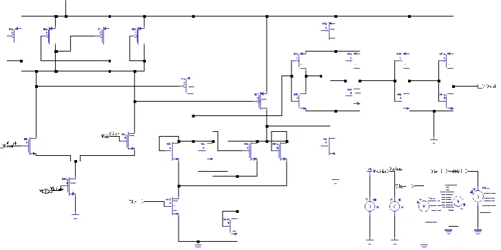
3. Tail Comparators
(a)Single tail comparator(Single Clocked)
(b)Double tail comparator(Double Clocked)
(a)Single tail comparator:
During reset phase, when clk=0, tail MN5 is off and both the reset transistors MP2 and MP4
are on and pull both the output nodes out1 and out2 to VDD which indicates a start condition
having a valid logic level in the reset phase. During comparison phase, when clk= VDD, the
transistors MP2 and MP5 are off, so that the out1 and out2 nodes starts discharging with
different rates depending on the applied inputs Vin-- and Vin++. Assuming Vin++>Vin--,
since the transistors are of same size, MN4 transistor will turn on faster than MN3 so that
out1 discharges faster than out2. When out1 discharges down to VDD-|Vthp| before out2, the
corresponding PMOS transistor MP3 turns on pulling the other output node out2 to VDD.
Thus the latch regeneration which is caused by back to back inverters starts. Thus, Out2 will
be pulled back to VDD and Out1 will be discharged to ground. If Vin++ < Vin--, the circuits
[image:6.595.78.533.386.632.2]works vice-versa. [5]
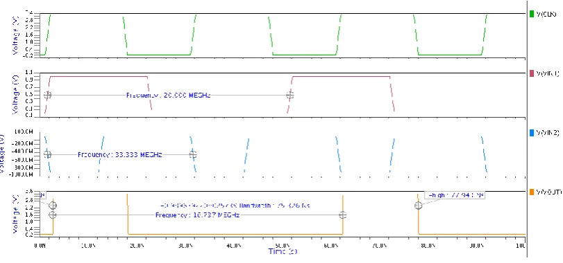
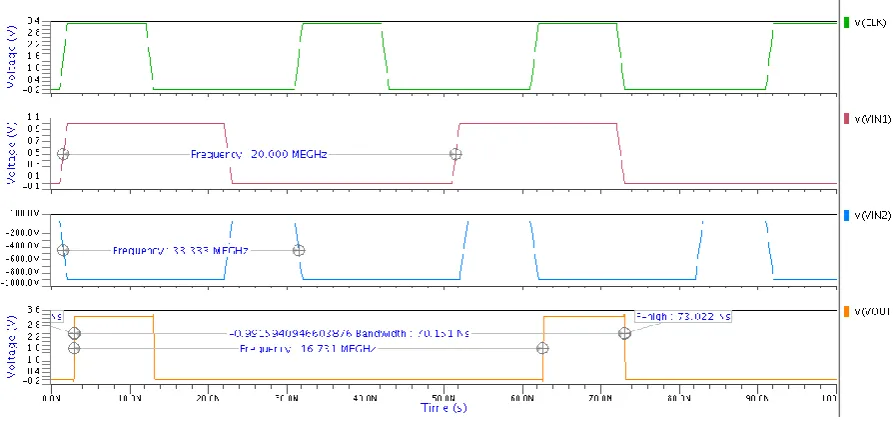
Fig 10. Transient analysis of single tail comparator
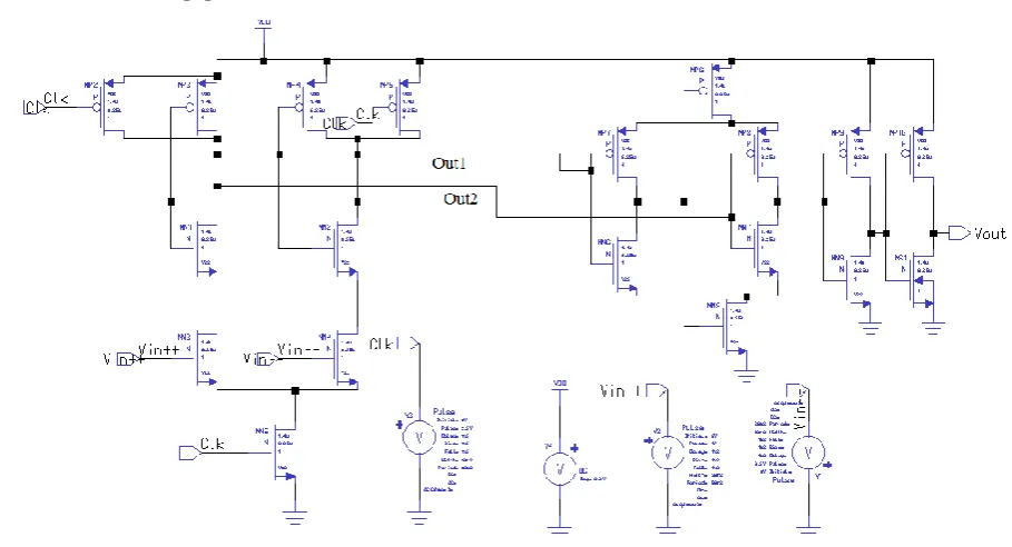
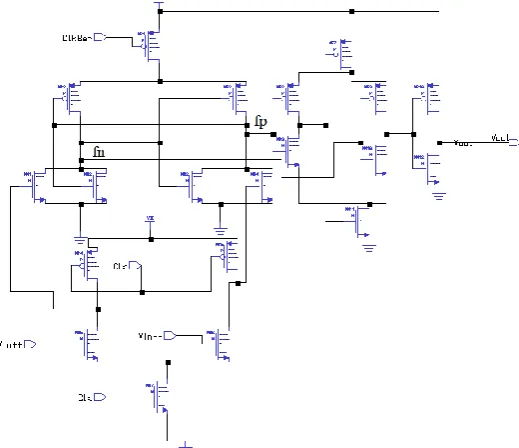
(b) Double tail comparator:
During reset phase, CLK = 0, thus the two tail transistors MN7, and MP1 are off, and the
transistors MP5 and MP4 are on so that the two nodes fn and fp will be pre charged to VDD,
which in turn causes transistors MN1and
MN4 to discharge the output nodes to ground. During decision-making phase CLK=VDD,
the transistors MN7 and MP1will be turned on, and both the PMOS transistors MP5 and MP4
will be off and voltages at nodes fn and fp start to drop with different rates. [5]
4. Clocked latch comparator
The proposed design is shown in Fig 14. It retains all important features of a comparator as
can be obtained in [6] besides offering high speed and removing dead time issue. The two
Fig 11. Double tail comparator
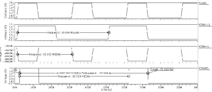
Fig 12. Transient analysis of double tail comparator
MP8 are used which at the beginning of the reset phase (clk=0) are turned OFF since PMOS
transistors MP6 and MP9 pre-charge the output node to VDD. During the evaluation phase
(clk=1) the tail transistor NMOS MN9 turns ON and the output nodes start to drop at
different rates based on the input voltages at transistors MN5 and MN6. The higher input
voltage transistor will draw more current which drops the voltage at its drain terminal,
turning ON either of the control transistors high keeping one control transistor completely
OFF. This arrangement will make one of the output terminal discharges completely to the
ground potential and keeps the other output node at a higher potential. Extra two NMOS
in saving static power consumption.
[image:9.595.74.520.98.700.2]Fig 13. Clocked latch comparator
Fig 14: Transient analysis of clocked latch type comparator
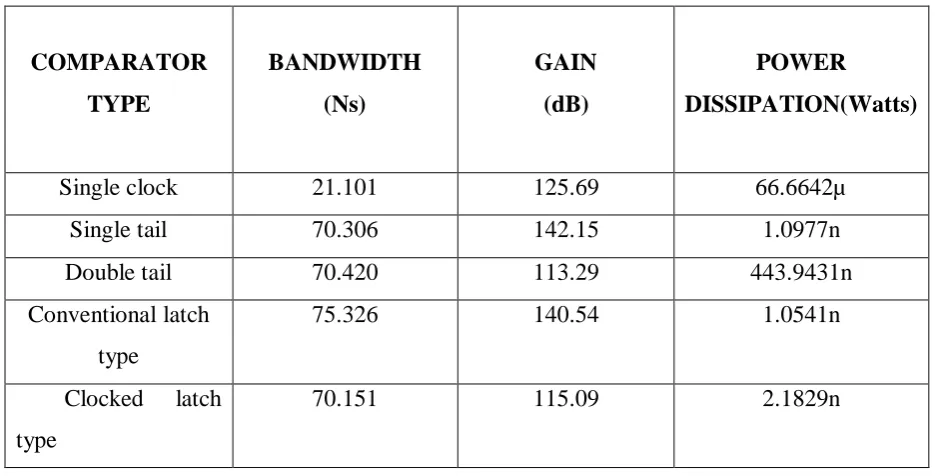
[image:9.595.81.528.290.502.2]III. RESULTS AND COMPARISION COMPARATOR TYPE BANDWIDTH (Ns) GAIN (dB) POWER DISSIPATION(Watts)
Single clock 21.101 125.69 66.6642µ
Single tail 70.306 142.15 1.0977n
Double tail 70.420 113.29 443.9431n
Conventional latch
type
75.326 140.54 1.0541n
Clocked latch
type
[image:10.595.64.532.80.318.2]70.151 115.09 2.1829n
Table 1: Comparison results
After analysing few of the CMOS Comparator schematics, the Transient and AC analysis
provided the parameters such as bandwidth, gain, power dissipation and the measured values
are tabulated in the Table 1. Therefore, the clocked latch type comparator gives reliable
results with power dissipation of 2.1829nW and again of 115.09dB. Single tail Comparator is
also another schematic which gives novel parameter values.
REFERENCES
[1] HeungJun Jeon Yong-Bin Kim, “A CMOS Low-power Low-offset and High-speed Fully
Dynamic Latched Comparator,” IEEE International SOC Conference, pp. 285, September
2010.
[2] Yatish Lavania, “A Low Power Encoder and Comparator Design of 5 Bit Flash ADC,”
NIT, Rourkela, 2013.
[3] Wazir Singh, “Study and Design of Comparators for High Speed ADCs,” Thapar
University, Patiala, 2011.
[4] Shilpi Singh, “A Novel CMOS Dynamic Latch Compartaor for Low Power and High
Speed,” International Journal of Microelectronics Engineering(IJME), Vol.1,No.1,2015.
Tail Comparator using HSPICE,” International Journal of Electronics and Electrical
Engineers(IJEEE), Vol. No.7 Issue 2, July-December 2015.
[6] H. Jeon and Y. Kim, “A novel low-power, low-offset and high-speed CMOS dynamic
latched comparator,” Analog Integr Circ Sig Process, vol. 70, pp. 337-346, July. 2011.
[7] Phillip E. Allen, Douglas R. Holberg, “CMOS Analog Circuit Design,” Third Edition,
Oxford University Press,Inc,2002.
[8] Rameshkumar.R, Bharathiraja.S. , “A Comparative Analysis of HighSpeed Dynamic
Comparator in 180nm and 90nm using H-spice,”
IJISER Vol 1 Issue 11 Dec 2014.
[9] Carlos J Solis, Gladys O. Ducoudray, "High Resolution Low power 0.6μm CMOS
40MHz Dynamic Latch Comparator," 53rd IEEE Intemational, Department of Electrical and
Computer Engineering, Aug. 2010.
[10] Anush Bekal, Rohit Joshi, Manish Goswami, Babu .R.Singh and Ashok Srivatsava, “An
Improved Dynamic Latch Based Comparator for 8-Bit Asynchronous SAR-ADC,” 2015
IEEE Computer Society Annual Symposium on VLSI.
[11] T. Xingyuan, Z. Zhangming, and Y. Yintang, “An offset cancelation technique in a
switched-capacitor comparator for SAR ADCs,” J.Semicond., vol. 33, no. 1, Jan. 2012, Art.
ID 015011.
[12] N. Mehan, A. Kumar, K. Kohli, and N. Sharma, “Offset reduction of CMOS based
Dynamic Comparator by using charge storage techniques---A comparative study,” Int. J.
Innovate. Res. Compute. Commun. Eng., vol. 1, no. 4, pp. 918-924, June. 2013.
[13] Behzad Razavi, “Design of Analog CMOS Integrated Circuits,” Tata McGraw-Hill,