Design and Implementation of CAN Bus Controller
on FPGA
Vaibhav Bhutada1, Shubhangi Joshi2, Tanuja Zende3
1, 2, 3
Asst. Professor, Department of Electronics & Communication Engineering, Shri. Chhatrapati Shivaji College Of Engineering, Pune.
Abstract: This paper describes the design, simulation and FPGA implementation of a protocol controller for the Controller Area Network (CAN) 2.0 which transmits and receives data at 1Mbps speed. It also going to deal with the design process of the FPGA, coding, simulating, testing and finally programming the FPGA. The CAN Controller designed will function as the interface between an application and the actual CAN bus. The RTL based design of CAN controller is implemented using Verilog HDL. The design is realized physically with electronic design automation (EDA) tools. Logic Equivalence is verified and Simulations are made at each level to verify the implementations. Model Sim SE6.3f will be used for functional simulation and Xilinx ISE tools will be used for synthesis and performance analysis.
I. INTRODUCTION
Controller Area Network (CAN) 2.0 is a serial communication bus originally developed for the automotive industry applications to replace the complex harness wiring by a two-wired bus.
The specification allows signaling rates of up to 1 Mbps and features high immunity to electrical interference and ability to self-diagnose and repair data errors.
Although initially developed for use in the automotive industry, its use quickly spread to a wide variety of embedded systems applications like industrial control where high-speed communication is required.
These features have extended the range of applications to variety of industries such as automotive, marine, medical, manufacture, military, aerospace, etc.
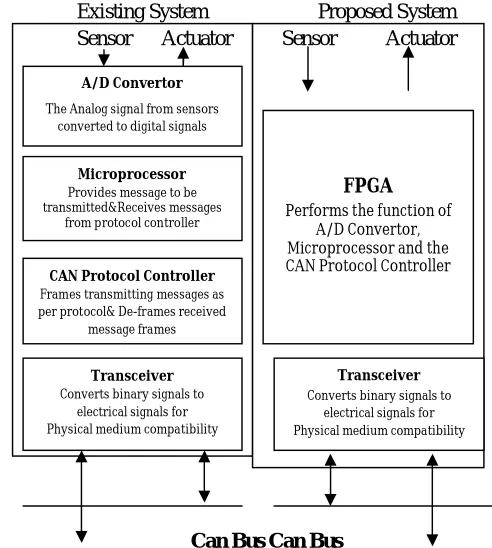
[1]The main task of this project is to implement the functionality of CAN controller on FPGA Board. All modules designed must conform to the CAN specification for the data transfer rate of 1 Mbps. Fig. 1 shows the block diagrams of existing and proposed CAN controller architecture.
The existing system is consist of an A/D convertor, a microprocessor, a CAN protocol controller and a transceiver. The CAN Protocol Controller receives unformatted message from the microprocessor, frames the messages as per the protocol specifications and also de-frames the received CAN message frames.
Existing System Proposed System Sensor Actuator Sensor Actuator
Can Bus Can Bus
Figure 1: Existing & Proposed CAN bus Controller architecture.
II. SYSTEM DESIGN OF CAN CONTROLLER A. Functional Block Diagram
[image:3.612.173.419.77.351.2]The functional block diagram for the controller is as shown in the following figure:
Fig. 1 Internal Block diagram of CAN Controller
This CAN controller is designed with structural design approach where individual modules are designed first and connected to each other in the top module.
The various functional blocks in the diagram are described as follows:
1) Host CPU: This is the interfacing application which provides the CAN controller with the data to be transmitted across the CAN bus and also reads the received messages from the controller.
2) Interface: The host application and the CAN controller is interfaced with an 8-bit data bus to transfer the message to the controller’s transmit buffer, an 8-bit data read bus which reads the messages received from the controller’s receive buffers and status signals to perform the requisite handshaking for these operations[10].
3) Parameter Registers: The code parameter, mask parameter and the Re-Synchronization Jump Width (SJW) specified for the CAN node is stored in this register.
4) TX Buffers: There is one transmit buffer with 10 registers of 1 byte each. The controller receives the message to be transmitted from the host CPU and stores the message in the transmit buffer before further message processing takes place.
5) Data / Remote :Frame Generator: Data / Remote Frame Generator is responsible for generating the message frame as specified by the CAN protocol.
FPGA Performs the function of
A/D Convertor, Microprocessor and the CAN Protocol Controller
Transceiver
Converts binary signals to electrical signals for Physical medium compatibility
A/D Convertor
The Analog signal from sensors converted to digital signals
Microprocessor
Provides message to be transmitted&Receives messages
from protocol controller
CAN Protocol Controller
Frames transmitting messages as per protocol& De-frames received
message frames
Transceiver
6) Parallel to Serial Converter: Serialization of the message to facilitate the CRC computation is done by this unit.
7) TX CRC Generator: Before transmission, this unit computes the CRC for the message to be transmitted. The generated CRC frame is appended to the message being transmitted before bit-stuffing is performed. The CRC Sequence which is transmitted as a part of the message frame is given by the remainder of this polynomial division.
8) Bit Stuff Unit: This unit performs bit-stuffing as specified by the CAN protocol, making the message suitable for transmission across the CAN network [10].
9) Error Frame Generator: Generates Error frame whenever error condition occurs. Error confinement measures are also taken care of to ensure the accuracy of the controller’s performance and its further participation in the CAN network.
10) Serialized Frame Transmitter: The data/ remote frame or the error frame or a dominant bit during the acknowledgment slot based on the prevalent conditions is transmitted by this unit.
11) Message Processor: This is the central unit which provides all the control and the status signals to the various other blocks in the controller. This unit routes the different signals generated in various blocks to the necessary target blocks.
12) Arbitration Controller: The arbitration controller indicates the arbitration status of the node.
13) Synchronizer: This unit performs the bit timing logic necessary for synchronizing the CAN controller to the bit stream on the CAN bus. The recessive to dominant transition edges present on the received bit stream are used for synchronization and re-synchronization.
14) Bit De-stuff Unit: This unit performs the de-stuffing of the messages received from the CAN network. This unit also extracts the relevant information from the received message.
15) RX CRC Generator: After reception, this unit computes the CRC for the message received.
16) Cyclic Redundancy Checker: This unit compares the generated CRC for the received message with the CRC frame received by the node. An error is generated if the two CRC values do not match.
17) Bit Stuff Monitor: The signal when astuff error when six consecutive bits of equal polarity are detected in the received message is indicated by this unit.
18) Form Checker: A form error is generated if any of the fixed-form fields in a received CAN message is violated. The fixed form fields include the CRC delimiter, ACK delimiter and the EOF field.
19) Bit Monitor: A CAN node acting as the transmitter of a message, samples back the bit from the CAN bus after putting out its own bit. If the bit transmitted and the bit sampled by the transmitter are not the same, a bit error is generated.
20) Acknowledgment Checker: During the transmission of the acknowledgement slot a transmitter transmits a recessive bit and expects to receive a dominant bit. If the node receives a recessive bit in the acknowledgement slot an ACK error is signaled. 21) Acceptance Checker: The incoming message ID and determines if the received frame is valid is checked by this unit.
22) Receive Buffer: There are two 10 byte buffers that are used alternatively to store the messages received from the CAN bus. This enables the host CPU to process a message while another message is being received by the controller.
B. CAN-Transceiver
Ready-to-use CAN-transceivers are available in many varieties, from low-power to fault-tolerant ones. Commercial-off-the-shelf transceivers. Here, we are using The PCA82C250 is the interface between a CAN protocol controller and the physical bus. Which provides differential transmit capability to the bus and differential receive capability to the CAN controller
C. Bit Timing Logic (Synchronizer)
1) This unit configures the timing parameters of the bit time for the CAN node. Each CAN node is configured individually to create a common bit rate for all the nodes on the network even though the CAN nodes’ oscillator periods may be different. 2) Synchronizations and re-synchronizations are performed on the recessive to dominant transition edges. The purpose is to
control the distance between edges and Sample Points.
3) The design for the bit timing and synchronization unit involves the calculation of the time quanta required for the Bit timing Parameters, which are the Synchronization Segment, Propagation Segment, Phase Segments 1 and 2 and the Synchronization Jump Width (SJW) [11].
4) Calculation of minimum permissible time for the Propagation Segment Physical interface delay = 100 ns
= 5*10-9 * 20
= 100 ns
Total propagation delay involved in back and forth bit transmission: = (Interface delay + physical bus delay) * 2 = (100 + 100) ns * 2
Total propagation delay = 400 nsWith a baud rate prescaler (BRP) value of 1, the CAN system clock frequency is calculated to be 10 MHz’s the value of a time quantum is given by the CAN system clock period and is given to be 100 ns. With the CAN bit rate being 1 Mega bits/second, and the time quanta/bit being 100 nanoseconds, the total number of time quanta per unit bit time is
= 1 Mega bits per seconds / 100 nanoseconds = 10 time quanta per unit bit time
Number of time quanta for Propagation Segment = (Total propagation delay) / (One time quanta)
= 400/ 100
= 4 time quanta.
5) With the total time quanta in a bit time being 10, 1 time quantum is reserved for Synchronization Segment and 4 time quanta are reserved for the Propagation Segment. This leaves (10-5) = 5 time quanta being reserved for the Phase Segments 1 and 2. As per the rule for designation of phase segments [1] which states that the value for phase segment1 must be equal to phase segment2, unless Phase Segment1 is less than the Information Processing Time (IPT). The value of IPT is always 2 time quanta. From this, the value of Phase Segment1 is determined to be 2 time quanta and the value for Phase Segment2 is determined to be 3 time quanta.
6) The value of Re-Synchronization Jump Width (SJW) is calculated as the smallest of 4 time quanta and Phase Segment1 and is thus calculated as 2 time quantum.
7) The values for all the segments of the nominal bit time and SJW are as follows: Synchronization Segment = 1 time quantum
Propagation Segment = 4 time quanta Phase Segment1 quanta = 2 time Phase Segment2 = 3 time quanta
SJW = 2 time quanta
III. DESIGN SIMULATION AND RESULTS: A. Verification Methodology
A simulation model for verifying the CAN controller has been designed with three CAN nodes instantiated on a network. The three CAN nodes have been instantiated as node 1, node 2, and node 3. In this simulation model, each CAN controller is capable of transmitting and receiving messages. This means that any of CAN controllers can be a master. The clock frequency used in this system is 10MHz and the CAN transmission rate is 1Mbit/s. The top module provides the nodes with the messages to be transmitted across the CAN network. The test bench module also provides the oscillator clock of 10 Mega Hz and the data at the CAN system clock of 1 Mega Hz for the CAN nodes. Apart from the above functions the top module Wire-AND’s the bit stuffed output streams of the CAN nodes.
B. Functional Verification
Fig.2 The Wire-ANDing mechanism of the CAN Bus
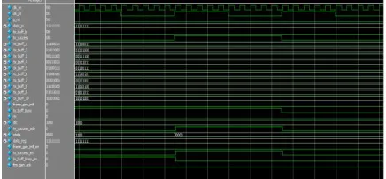
[image:6.612.188.426.287.408.2]2) Data and Remote Frame Framing: The CRC generation initialization is demonstrated in Fig.3. The Frame generation is initialized by the high assertion of the frame_ gen_intl signal. Based on the Data Length Code (DLC) and the Remote Transfer Request (RTR) bit the par_ser_data frame is generated. The par_ser_data frame is formed by the concatenation of the dominant Start Bit, the Message Identifier, the Control Field and the Data Field if it exists. Dominant bits are appended to the frame to counter for the trailing bits which are not defined by the message.
Fig.3 Frame generation
3) Bit Stuffing: The bit stuffing mechanism is demonstrated in Fig.4 With the initialization of bit stuffing the contents of the 98 bit register dt_rm_frm are transferred to a temporary register msg. The contents of the msg register are serialized and then checked for the bit Stuffing condition. At every positive edge of the clock the contents of the msg register are shifted left by 1. The left shifted bit is placed on the dt_rm_out bus which is connected to the CAN bus. A count of the bits in the original un-stuffed message stream is kept in the register bit_cnt. The stuffed bit stream being put out on the CAN bus has the Start Bit being transmitted first, followed by the message identifier’s most significant bit and so on.
Fig. 4 The bit stuffing mechanism
[image:6.612.200.415.502.635.2]Fig. 5 The Bus Arbitration mechanism
[image:7.612.183.431.329.464.2]5) Acknowledgement: During the transmission of the acknowledgement slot a transmitter transmits a recessive bit and expects to receive a dominant bit. Referring to Fig. 6 the bit time for ACK Slot is indicated by the high assertion of the ack_slt signal. This signal remains high throughout the bit time of the ACK Slot. During the ACK slot the transmitting node2 in this case, transmits a recessive bit, the other nodes in the network namely node3 transmit a dominant bit if it has been an error-free reception till that bit. With the bit on the CAN bus being the Wire-AND of the bits transmitted by all the nodes on the network, the bus bit sampled back by the transmitting station Node node2 is logic low.
Fig. 6 Acknowledgement
6) Signaling Transmission Success: The successful transmission of the message is indicated by the tx_success signal going high for one clock cycle. On successful transmission of the message the tx_buffer_busy signal goes low and the controller is ready to receive the next message for transmission. In case of an error during transmission the buffers are not reset and will continue to hold on to the current value until the message is transmitted successfully.
Fig. 7 The signaling of successful transmission
[image:7.612.198.416.536.637.2]Fig. 8 The bit synchronization mechanism
[image:8.612.199.415.250.371.2]8) Bit De-stuffing: The bit_destf_intl signal is asserted high to initialize the de-stuffing process. The message stream received is then de-stuffed to get the respective fields of the transmitted message. The serial_in register holds the synchronized stuffed serial bit stream received by the node.
Fig.9 The bit de-stuffing mechanism
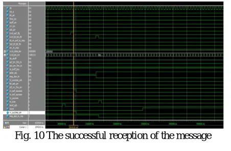
9) Signaling Reception Success
The successful reception of the message is indicated by the rx_success signal going high for one clock cycle.
Fig. 10 The successful reception of the message
IV. CONCLUSION AND FUTURE WORK A. Conclusion
The results obtained from the simulation of the design implemented in ModelSim SE6.3f, have been elucidated. Error-free transmission and reception of message frames has been demonstrated with two nodes instantiated on a network each taking turns to transmit messages. The detection and transmission of error frames in the event of an error has been demonstrated by inducing CRC in the messages. All the basic functions involved in the transmission and reception of the message as per CAN 2.0 protocol have been demonstrated and found to be meeting the requirements. The Logic Equivalence has been checked and the final design is proven to be logically equivalent to the RTL code. The design meets timing requirements specified. Thus the pre FPGA implementation of a basic protocol controller for CAN 2.0 protocol has been simulated and verified successfully.
B. Future Work
[image:8.612.196.422.417.565.2]And final verification of the design as the Listen Only mode where the node has no influence on the bus, no active error flags, no overload flags, and no acknowledgement can be sent, but it can receive
Messages, a Self Test mode [4] and Self Reception Request to enable full node testability without any other active node, and a Sleep mode with reduced power consumption.
The CAN controller is designed to operate at a fixed bit rate of 1Mbps. By providing a Programmable Bit Time Logic with programmable bit rate, the controller can be extended to operate at multiple bit rates. The controller can be further extended by making the propagation segment and phase segment lengths programmable. More functionality can be incorporated into the controller by enabling single or triple sampling of the bit.
The optimized hardware for the CAN controller can be configured, making the hardware available for further use.
REFERENCES
[1] S. Corrigan, “Technical Article: Introduction to the controller area network (CAN),” Texas Instruments, Application Report SLOAIOI, 2002.
[2] Sunitha A and Raghu MC, “Implementation of Can Bus Based System -on-Chip on Altera FPGA,” IJSR - International Journal OfScietific Research, Volume 3, Issue 5, May 2014.
[3] Deepika.T.P and Bhagya.P, “Dual Redundancy CAN-bus controller based on FPGA,” International Journal of Scientific and Research Publications, Volume 4, Issue 5, May 2014.
[4] Amit Kumar Bhadrawat and Sourabh Sharma, “BIST based can Bus Control System ImplementedInto FPGA,” International Journal of Innovative, Technology and Exploring Engineering (IJITEE)Volume-4 Issue-5, October 2014.
[5] StijnWielandt, Geoffrey Ottoy, Jean-Pierre Goemaere, Nobby Stevens and Lieven De Strycker, “Integration of a CAN bus in an OnboardComputer for Space Applications,” 11th International Conference on DEVELOPMENT AND APPLICATION SYSTEMS, Suceava, Romania, May 17-19, 2012.
[6] PeterDzhelekarski, Volker Zerbe, and Dr. Dimiter Alexiev, “FPGA Implementation of Bit Timing Logic of CAN Controller,” 27th International Spring
Seminar on Electronics Technology
[7] José Rufino, Ricardo Pinto, and Carlos Almeida, “FPGA-based Engineering of Bus Media Redundancy in CAN,”ICC 2008. [8] Daniel Mannisto, Mark Dawson, “An Overview of Controller Area Network (CAN) Technology,”mBus, 2003.
[9] Steve Corrigan, “Introduction to the Controller Area Network (CAN) – Texas Instruments Application Report,” SLOA101, 2002. [10] KarthikRanganathan, “RTL System Design of CAN 2.0A Controller, Master’s Thesis,” Texas Tech University, Lubbock, TX, 2005. [11] Stuart Robb, “CAN Bit Timing Requirements – Motorola Semiconductor Application Note,” AN1798, 1999.