Asynchronous Serial Interface
(ASI)
Technical Reference Manual
Flin-
HEWLETTThe Printing History below identifies the Edition of this Manual and any Updates that are included. Periodically, update packages are distributed which contain replacement pages to be merged into the manual, including an updated copy of this Printing History page. Also, the update may contain write-in instructions.
Each reprinting of this manual will incorporate all past updates; however, no new information will be added. Thus, the reprinted copy will be identical in content to prior printings of the same edition with the user-inserted update information. New editions of this manual will contain new information, as well as updates.
First Edition ... November 1982 Second Edition... June 1983 Update 1 ... September 1983 Update 2 ... .... ... ... ... December 1984
NOTICE
The information contained in this document is subject to change without notice.
HEWLETT-PACKARD MAKES NO WARRANTY OF ANY KIND WITH REGARD TO THIS MATERIAL, INCLUDING, BUT NOT LIMITED TO, THE IMPLIED WARRANTIES OF MERCHANTABILITY AND FITNESS FOR A PARTICULAR PURPOSE. Hewlett-Packard shall not be liable for errors contained herein or for incidental or consequential damages in connection with the furnishing, performance or use of this material.
This document contains proprietary information which is protected by copyright. All rights are reserved. No part of this document may be photocopied, reproduced or translated to another language without the prior written consent of Hewlett-Packard Company.
Section I Page GENERAL INFORMATION
Physical Description ••..•.••••••••••.•.••.••••••.•.•.•••••..••••... 1-1 1-1 1-3 1-3 1-3 1-3 1-4 1-4
Functional Description ... . Equipment Supplied ••••..•••.•.
Identification ...•..••
The Product ...•••••.. • • • • • • • • • e . • • •
I nt er face Card ••••.•...••••..•...••.•...••• Manuals ...•.
Specifications.
Section II INSTALLATION
Computation of Current Requirements ....•..•. Firmware (EPROM> Installation ...
Configuration Switch Definitions .. Single Text Termination Switch. Hard-Wired Switch.
No Parity Switch ..
8-Bit Data Rate Switch ..
Baud Rate Switches •..
liD
Channel Interface .. Peripheral DeviceInstallation .. Start Up .... . Reshipment .. .
Section III
Interface.
PRINCIPLES OF OPERATION
Functional Theory of Operation .•. Memory Address Space ..
liD
Address Space ... Configuration Jumpers.Interfacing to BIC ...•.•....
Interfacing to RS-232-C/RS-423 Devices .. Z-80A Subsystem ..••.•...•..
CTC (Counter/Timer Circuit) ....•••.•.•.•.•..•...•...•••••..•.. 3-11 Priority Interrupt Structure .•••.•.•....••.••....•.••••••.•••. 3-15
EPROM ••....••.••..••.••••....•.•••..•.•.••.•...•••...••••.•• 3-15
Power Up Default State Switches ••...•..••...•.•..•••.••.•.•. 3-15 lID Register . . . 3-15 Reset Circuit . . . 3-17
Wait State Generating Circuit •.•••.••..•...••....•..••..••... 3-18
Section IV PROGRAf1"1ING
Page
AS! Programmable Features ...••.•....•...•...•...•... 4-1 Performance ... . 0 • • • • • • • • • • • • • • • • • " • • • • • • • • • • • • • • • • • • • • • • • • •• 4-2 Transact ions . . . ' . 1 • • • • • • • • • • • • • • • • • • • • • • • • • • • • • • • Ii • • • • 4-2
Connect Logical Channel (CLC) Request Format ...•... 4-3
Capabilities, . . . · .... 4-4
Receive Character Processing .•...• 4-5 Receive Error Conditions ...•...•...•.•...• 4-7 Software Handshake with the Device ...•..•...•....•...•...• 4-7 Host ENQ/ACK Handshake ...•...••... 4-8 Device ENQ/ACK Handshake ...•..•..•••.. ~ .••.•••...•... 4-8 Host X-ON/X-OFF Handshake ...•...•... 4-8 Device X-ON/X-OFF Handshake ....•...• 4-9
Ed i t Mode... 4-9
Bae k space . . . 4-9
Line Deletion . . . 4-10
Character Stripping ...•... 4-10 Single Text Termination ...•...•... · ... 4-10 Double Text· Terminat ion ..•...•.••... 4-11 Prompt Sequence Detect ion ... ' •....•...•... 4-11 End-On-Count Termination ... 4-11 Alert 1 Read Mode ...•... 4-12 Type Ahead and Echoing ...•...•... 4-12 Receiving Transparent or Binary Data ...•... 4-14 Function of Read Request Length ...•..•... 4-14 Host Initiated Text Termination ...•..•...•... 4-15 Transmit Character Processing ...•.•..••..•... 4-15 Automatic Output Separators Appendage ...•.•...••... 4-15 Transmitting Transparent or Binary Data ...•... 4-16 Transmi t Hardware Handshak i ng ... 4-16 Force Restart of the Transmi t ter ....•...•...•...•... 4-16
Buffer Flu5hin9~ ....••.•••••.•••...•••.•••..••••••••••••....•.•• 4-16
Programming the Receiver and Transmitter ... : ... 4-17 Parity in Transmitted or Received Data ...•... 4-18 Break Detection and Generation ... 4-18
Firmware Control of the Modem Signal ..•..•....•.•...••... 4-21
Full-Duplex Modem . . . " ... : ... 4-22
Full-Duplex Modem Timi ng Diagrams •.•.•••....•.•••... ~ •.••...• 4-22
Addi t ional opt ion5 . . . " . • . . . ' . . . ' . . . 4-29 Error Handling_ . . . '. ... . " ... 4-29
Quoting Character Mode Option ••...••.•... ; ... 4-29 Conditional Output Separators Appendage ...••••...•.•.•... 4-30 Signal Charact'er ... I " ' • • • • • • • • • • • • • • • • • • • • • • • • • • • • " . " . " . ' . . . .• 4-30
Null Character Insertion ..•..•..•• : •••...•...•... 4~30
Asynchronous Events ...•.••...•...• ~ ... ~ .... 4-30 Solici ted Event5 ... I " • • • I" • • • • • • • • • • • • • • · .. ' . · • • • • " • • • • 4-32 Diagnost iC5 . • • '.' • • • • • • • • • • • • • • • • • • • • ' • • • • • • • • • • • • • • • " • • • • • • " • • • • • • • 4-33 Configuration Switch Definitions ...•...•.•...•...• 4-34 Baud RateSwi tches ...•••..•...•... 4-35 8 - Bit Da t a Sw i t c h. . ... . . • . • . . . ... . . 4 -35
No-Par i ty Swi tch ... " ... " . . . " . . . it • • • 4-35 Hardwired Swi tch . . . • . . . 4-36
Single Text Termination Switch ...•.•....•.•.... 4-37 Transaction Request Block Subfunctlon Definitions ..•... 4-37 Read Device Data, Request Code = 1 .. it . . . ~ • • • 4-37
Write Device Data, Request Code
=
2 •...•... 4-37 Cont rol Device, Request Code = 3 ...•... 4-38 Read Card Information, Request Code=
4 ..••..•...•... 4-38Subfunct ion 0 . . . a a • • • a . . . • :" • • " • • a-a a • • '"'-4-39 Subfunctions 1 through 32 ...•...•...•... 4-39 Subfunct ion 250. Get the Card RAM ..•...• 4-39 Subfunction 251. Get the Card Read Register ...•.. 4-39 Subfunct ion 252. Get the Card Wr i te Register ... i • • • • • • • 4-39
Subfunction 253. Get the Card Switch Setting ... 4-40 Subfunction 254. Get Card Status ... ~ ... 4-40 Subfunction 255. Read Modem Line Status ..•..•... ~ ... r • • • 4-41
Write Card Configuration, Request Code
=
5 ... , .... 4-41 Subfunct ion 0 .. ;. ... ~ ...•... 4-42 Subfunction 1 .Subfunction 2. Subfunction 3. Subfunction 4. Subfunction 5. Subfunction 6.
Subfunction 7. Subfunction 8.
Subfunction 9.
Configure ASI-to-Device Control ... 4-45 End-On-Count Length •...•... ~ ... 4-45 Alert 1 Read Mode ...•..•... 4-46 Modem Connect ion Mode ... 4-46 Transmission Mode ...•... 4-47 Backspace Character ....•....•..•... io • • • 4-A7
Subfunction 12. Number Of Stop Bits .•••••..•••••••••••••••. 4-51 Subfunction 13. Parity ..••••••••••••••••.••••••••••••••••.. 4-51 Subfunction 14. Modem Connection Timer •••••••••••••••••••.. 4-52 Subfunct ion 15. No Acti vi ty Timer •••••••••••••••••••••••... 4-52 Subfunction 16. Lost Receiver Ready Timer ••.•••.••••••..•.• 4-52 Subfunction 17. Gap Timer .•.•••...•..•••••.•••••••••..•.... 4-52 Subfunction 18. Host ENQ/ACK Timer •••.•••.•••••.•••.•....•. 4-52 Subfunction 19. Break Generation Timer ••••••••••••.•••.•.•. 4-52 Subfunction 21. Host and Modem Interrupt Mask •••••.•••... 4~53
Subfunction 22. Host X-ON/X-OFF Characters .•••••••.••... 4-54 Subfunction 23. Device X-ON/X-OFF Characters •••.••••••....• 4-55 Subfunction 24. Host ENQ/ACK Characters ••••••.•..••.•••.•.• 4-55 Subfunction 25. Host ENQ/ACK Pacing Counter ••••••••... 4-55 Subfunction 26. Device ENQ/ACK Characters .••••.•••... 4-56 Subfunction 27. Single Text Terminator for Echoing CR-LF ... 4-56 Subfunction 28. Output Separator ..•.•••••..• : ••.•..•••...•. 4-56 Subfunct ion 29. Double Text Terminator ••.•.••.•...••.... 4-56 Subfunct ion 30. Prompt Sequence ..••••.•••..••••..••..•.•... 4-57 Subfunction 31. Additional Options ... 4-57 Subfunction 32. Single Text Terminator ••...•..••...•... 4-58 Subfunction 33. Card Write Register ...••••...••.•...•.••... 4-58 Control Card, Request Code
=
6 ...•..•...•.•...•... 4-59 RTS and WTC Block Definitions •...••.••••.••.••..•.••.•••••.••..• 4-60 Event Block Description ....•••••.••....•...••..•••.•...•.•... 4-61 Read Status (RS) Block Def i ni t ions ..•...•...••••..••... 4-64I dent.i ty In format ion Bloc k Def i ni t ion. ~ •....•••..•.••... 4-67 De·fault ASI Co·nfigurations ••...•••...•....•...•..•...•... 4-68 Subfunction Assignment Sunmary ...••..•.•... 4-71
Read Device Data . . . 4-71 Wri te Device Data . . . 4-71 Cont rol Device . . . 4-72 Read Card Information .••.•...•..••...•... 4-72 Write Card Configuration ... 4-73 Cent rol Card . . . 4-74
Section V Page
MA I NTENANCE. . . • . . . • . • . . • . • . . . • • . . . • • • . . . • • . . • • . • . . . 5-1
Section VI
REPLACEABLE PARTS
Page
Section VII
Page
SCHEMAT Ie DI AGRAMS ••••••••• a . • • • • • • • • • • • • • • • • • • • • • • • • • • • • • • • • • • • • • • • 7-1
Appendix A
Page
GENERAL INFORMA TION
I~'!'!.jf'
This manual provides general information, installation, theory. of operatio.n, maintenance instruc-tions, replaceable parts information, and servicing diagrams for the Hewlett-Packard HP 27128A Asynchronous Serial Interface (AS!). This section contains general information concern-ing the ASI, and includes a description and specifications.
PHYSICAL DESCRIPTION
The HP 27128A Asynchronous Serial Interface (AS!) is shown in figure 1-1 and consists of a printed circuit card, a cable, and an installation manual.
FUNCTIONAL DESCRIPTION
The HP 27128A Asynchronous Serial Interface (AS!) provides an asynchronous serial communica-tions link between a Hewlett-Packard computer system and an EIA RS-232-C/RS-423-compatible or CCITT V.24/V.28-compatible terminal or other similar peripheral device. The ASI allows modem control or direct interfacing to the peripheral device.
Figure 1-2 shows a Hewlett-Packard computer system using CHANNEL I/O and the AS!. (CHANNEL I/O is a Hewlett-Packard standard defining the physical and electrical characteristics for an I/O system consisting of an I/O channel, an I/O channel adapter, and I/O cards. The ASI is one of the I/O cards.)
Note that the computer system CPU and memory communicate directly along a Memory/Processor Bus (MPB). I/O data to/from peripheral devices reaches the CPU/memory through the I/O channel, the I/O channel adapter, and an I/O card such as the ASI card. The I/O data is received from and transmitted to peripheral devices by the I/O card, which converts device-specific data to a for-mat compatible with the I/O channel~ and thus the computer. The I/O channel adapter (see figure
MEMORY
I
1/0
CHANNEL ADAPTER
I
1-1
I~
I
~ ,--_..L.-_....,I~ I/O I~ CARD
len
I/O
CARD
I/O
CARD
EQUIPMENT SUPPLIED
The standard HP 2712 SA ASI Interface consists of the following items (see figure 1-1):
ASI card, part number 2712S-60001
Five meter female RS-232-C cable, part number 27128-63002 Installation manual, part number 2712S-90001
The following option is available with the HP 2712SA product:
Option 001:
~~
Five meter male (modem) RS-232-C cable, part numbe~OOl
r;:
J.~)f>·,(f!IDENTIFICA TION
The Product
Up to five digits and a letter (2712SA in this case) are used to identify Hewlett-Packard products. The five digits identify the product; the letter indicates the revision level of the product.
Interface Card
The interface card supplied with the HP 2712SA product is identified by a part number
marked on the card. In addition to the part number, the card is further identified by a letter and a
four-digit date code (e.g., A - 2322). This designation is placed below the part number. The letter identifies the version of the etched circuit on the card. The date code (the four digits following the letter) identifies the electrical characteristics of the card with components mounted. Thus, the complete part number on the ASI card could be:
2712S-60101 A-2322
dif-Manuals
The Installation Manual (part number 27128-90001, supplied with the HP 27128A product) and this manual (HP 27128 Technical Reference Manual, part number 27132-90001) are identified by name and part number. (Note that this manual is part of the HP 27132A Technical Reference Package.) The name, part number, and publication date are printed on the title page of each manual. If the manual is revised, the publication date is changed. In this manual, the "Printing History" page (page ii) records the reprint dates and manual update record. Reprint dates for the Installation Manual are printed on the title page.
SPECIFICA TIONS
Table 1-1 lists the specifications of the ASI.
Ta ble 1-1. Specifications
FEATURES
*
Microprocessor subsystem (Zilog Z-80A) is programmed to perform the following functions:Parity generation and checKing
BacKspace and line delete processing
Host and device character handshake
Termination character detection
Full-duplex modem handshake
*
EIA RS-232-C, RS-423, and CCITT V.24, V.28 compatibility*
Modem control signals configurable by software to allow operation with most available modems*
Full-duplex, echoplex, or simplex operation*
Data rates selectable up to 19,200 bits per second (baud)Table 1-1. Specifications (Continued)
*
Character buffering: up to 500· byte!! in tran!!mit mode,
up to 480 byte!! in receive mode
*
Can !!end or receive 5, 6, 7, or 8 bit!! per charecter,
plu!! even, odd, or no parity
*
Will operete with 1, 1.5, or 2 !!top bit!!
*
Will detect end generete BREAK !!ign!ll
PHYSICAL CHARACTERISTICS
Size:
193.04
mmlong by 171.45
mmwide
by 16.383
mmthick
(7.6 by 6.75 by 0.645 inche!!)
Weight:
203.6 grem!! (0.448 pound)
lID
Channel Interconnects: 80-pin connector, J1
Device Interconnect!!:
50-pin connector, J2
POWER REQUIREMENTS
Voltage
+5V
+12V
-12V
Current
1.29A
54mA
73mA
Power Di5sipation
6.45W
O.65W
0.87W
[image:13.623.67.551.106.733.2]INSTALLATION
1-~---~[[]
This section provides information on installing and checking the operation of the ASI.
COMPUT A TION OF CURRENT REQUIREMENTS
The ASI circuit card obtains its operating voltages from the host computer power supply through the I/O channel. Before installing the card, it is necessary to determine whether the added current will overload the power supply. The current requirements of the card are listed in the power require-ments entry of table 1-1. Current requirerequire-ments for all other I/O cards can be found in the ap-propriate Technical Reference Manuals.
FIRMW ARE
(EP~OM)INST ALLA TION
I
CAUTIONI
SOME OF THE COMPONENTS USED IN THISPRODUCT ARE SUSCEPTIBLE TO DAMAGE BY ST A TIC DISCHARGE. REFER TO THE SAFETY CONSIDERATIONS INFORMATION AT THE FRONT OF THIS MANUAL BEFORE HANDLING THE CARD OR REl\10VING OR REPLACING COMPONENTS.
The EPROM and RAM are installed in a socket provided on the ASI card as shown in figure 2 -1.
Z80ACPU
BIC
Z80A CTC
Z80A
510/2 EPROM
SWITCH
RAM
Additionally, when installing or removing the EPROM or RAM, guard against bending or breaking the pins on the component. These pins also can become folded between the component and its socket, which would result in intermittent operation of the ASI. In most cases, a bent or damaged pin can be straightened with careful use of needle-nose pliers.
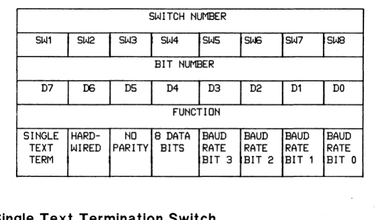
CONFIGURA TION SWITCH DEFINITIONS
Eight switches on the ASI card (see figure 2-1 for locations) allow you to select configuration op-tions. Switch definitions are shown in table 2-1.
Table 2-1. Configuration Switch Definitions
SWITCH NUMBER
SW1
SW2
SW3
SW4
SWS
SW:;
SW7
SWSBIT NUMBER
D7
00DS
D4
D3
D2
D1
DO
FUNCTION
SINGLE HARD-
NO
8 DATA BAUD
BAUD
BAUD
BAUD
TEXT
WIRED PARITY BITS
RATE
RATE
RATE
RATE
TERM
BIT 3 BIT 2 BIT 1 BIT 0
Single Text Termination Switch
If switch SW 1 is open, single text termination is enabled. See Section 4 for a discussion of single text termination.
Hard -Wired Switch
[image:17.613.75.450.299.519.2]No Parity Switch
If switch SW 3 is open, no parity is used. If the switch is closed, odd parity is programmed into the SIO. The other parity options may be selected programmatIcally. See Section 4 for a discussion of the parity options.
a-Bit Data Rate Switch
Switch SW 4 is used to set the character length. If this switch is open, the character length is 8 bits; if closed, the character length is 7 bits.
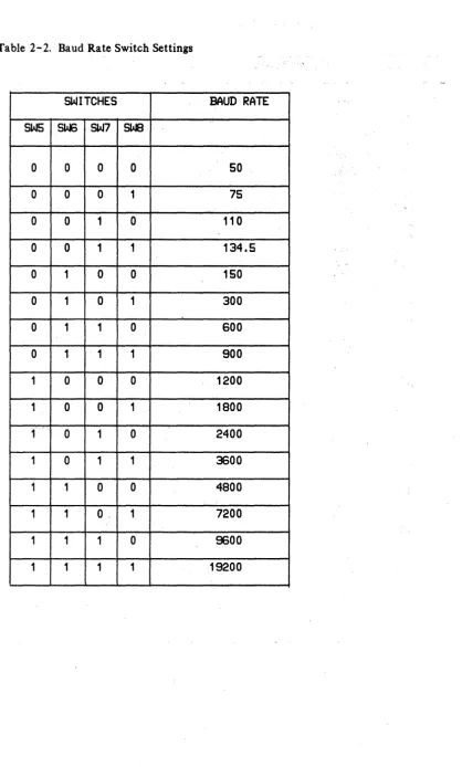
Baud Rate Switches
Switches SW5 through SW8 are used to select the baud rate of the ASI. The switch settings and corresponding baud rates are shown in table 2-2. Note that a 1 in table 2-2 signifies an open switch; a 0 means the switch is closed.
1/0
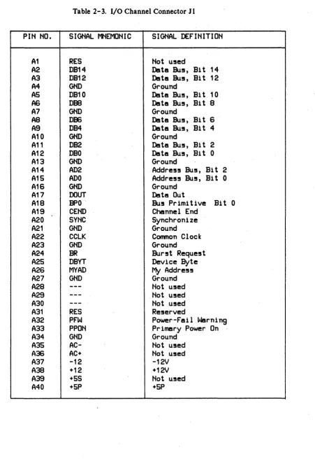
CHANNEL INTERFACE
All interface between the ASI and the host computer occurs on the I/O channel. An 80-pin con-nector (J 1) located on the ASI mates with a receptacle on the I/O channel. Connections to Jl are listed in table 2 - 3.
PERIPHERAL DEVICE INTERF ACE
Table 2- 2. Baud Rate Switch Settings
SWITCHES
BAUD RATE
SW5 SW:; SW7 SWB
0
0
0
0
50
0
0
0
1
75
0
0
1
0
110
0
0
1
1
134.5
0
1
0
0
150
0
1
0
1
300
0
1
1
0
600
0
1
1
1
900
1
0
0
0
1200
1
0
0
1
1800
1
0
10
2400
1
0
11
3600
1 1
0
0
4800
1 1
0,
1
7200
1
1 10
9600
[image:19.618.139.557.56.749.2]Table 2-3. I/O Channel Connector JI
Plti tiO.
SIGNAL MNEMOtilC
SIGNAL DEFltilTIOti
A1
RES
tiot u5ed
A2
DB14
-Deltl!! Bu5, Bi t 14
A3
DB12
Deltl!! BU5, Bi t 12
A4
GND
Ground
AS
DB10
Detl!! Bu!!, Bi t _ 10
AS
DBa
Deltl!! BU5, Bit 8
A7
GND
Ground
A8
DB6
Deltl!! BU5, Bit S
A9
DB4
Deltl!! BU5, Bit 4
A10
GtiD
Ground
A11
DB2
Deltl!! Bu!!, Bit 2
A12
DBO
Deltl!! BU5, Bit 0
A13
GtiD
Ground
A14
AD2
Addre55 BU5, Bit 2
A15
ADO
Addre55 BU5, Bit 0
A1S
GtiD
Ground
A17
DOUT
DatI!! Out
A18
BPO -
Bu5 Primitive Bit 0
A19
CEtiD
Channel End
A20
SytiC
Synchronize
A21
GtiD
Ground
A22
CCLK
Common Clock
A23
GtiD
Ground
A24
BR
Bur5t Reque5t
A25
DBYT
Device Byte
A2S
MYAD
My
Addre55
A27
GtiD
Ground
A28
---
tiot u5ed
A29
---
tiot u5ed
A30
---
tiot u5ed
A31
RES
Re5erved
A32
PFW
Power-Fail Warning
A33
PPOti
Prlmesry Power On
A34
GtiD
Ground
A35
AC-
tiot u5ed
A36
AC+
Not u5ed
A37
-12
-12V
A38
+12
+12V
A39
+5S
tiot u5ed
[image:20.613.58.509.60.736.2]Table 2-3. I/O Channel Connector Jl (Continued)
PIN NO. SIGNAL MNEMONIC SIGNAL DEFINITION
B1
---
Not usedB2 DB15 Data Bus, Bi t 15
B3 DB13 Data Bus, Bi t 13
B4 GND Ground
B5 DB11 Data Bus, Bi t 11
136 DBS Data Bus, Bit 9
B7 GND Ground
B8 DB7 Data Bus, Bi t 7
BS DB5 Data Bus, Bi t 5
B10 GND Ground
B11 DB3 Data Bus, Bi t 3
B12 DB1 Data Bus, Bi t 1
B13 GND Ground
B14 AD3 Address Bus, Bit 3
B15 AD1 Address Bus, Bit 1
B16 GND Ground
B17 UAD Unary Address
B18 BP1 Bus Primitive Bit 1
B19 CBYT Channel Byte
B20 POLL Poll
B21 GND Ground
B22 10SB I/O Strobe
B23 GND Ground
B24 ARQ Attention Request
B25 DEND Device End
B26 RST Reset
B27 GND Ground
B28
---
Not usedB29
---
Not usedB30 RES Reserved
B31 RES Reserved
B32 NMI Non-Maskable Interrupt
B33 SPON Secondary Power On
B34 GND Ground
B35 AC- Not used
B36 AC+ Not used
B37 -12 -12V
B38 +12 +12V
B39 +5S Not used
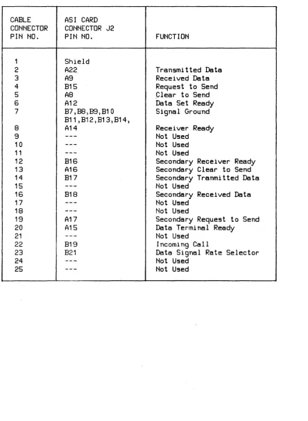
CABLE CONNECTOR PIN NO.
1 2 3 4 5 6 7 8 9 10 11 12 13 14 15 16 17 18 19 20 21 22 23 24 25
Table 2-4. RS-232-C Male Cable Pinouts
ASI CARD CONNECTOR J2 PIN NO.
Shield A22 A9 B15 A8 A12 B7,88,89,B10 B11,B12,B13,B14, A14 B16 A16 B17 B18 A17 A15 B19 B21 FUNCTION
Transmitted Data Received Data Request to Send ,Clear to Send Data Set Ready Signal Ground
Receiver Ready Not Used
Not Used Not Used
Secondary Receiver Ready Secondary Clear to Send Secondary Tranmitted Data Not Used
Secondary Received Data Not Used
Not Used
Secondary Request to Send Data Terminal Ready
Not Used Incoming Call
Data Signal Rate Selector Not Used
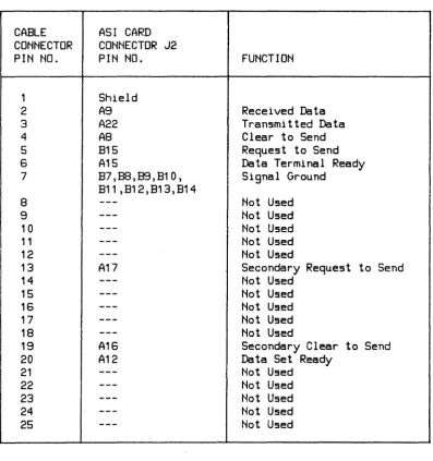
[image:22.615.70.515.100.707.2]Table 2-5. RS-232-C Female Cable Pinouts
CABLE ASI CARD
CONNECTOR CONNECTOR J2
PIN NO. PIN NO. FUNCTION
1 Shield
2 A9 Received Data
3 A22 Transmitted Data
4 AS Clear to Send
5 B15 Request to Send
6 A15 Data Terminal Ready
7 B7,BS,B9,B10, Signal Ground
B11,B12,B13,B14
8
---
Not Used9
---
Not Used10
---
Not Used11
---
Not UsedI
12 13---
A17 Not Used Secondary Request to Send14
---
Not Used15
---
Not Used16
---
Not Used17
---
Not Used18
---
Not Used19 A16 Secondary Clear to Send
20 A12 Data Set Ready
21
---
Not Used22 --- Not Used
23
---
Not Used24
---
Not Used [image:23.615.77.475.117.540.2]INST ALLA TION
I
CAUTIONI
AL WAYS ENSURE THAT THE POWER TO THE COMPUTER IS OFF BEFORE INSERTING OR REMOVING THE ASI CIRCUIT CARD AND CABLE. FAILURE TO DO SO MAY RESUL T IN DAMAGE TO THE ASI.
I
CAUTIONI
S01\1E OF THE COl\1PONENTS USED ON THE PRINTED CIRCUIT CARD ARE SUSCEPTIBLE TO DAMAGE BY STATIC DISCHARGE. REFER TO THE SAFETY CONSIDERA TIONS INFORMA TION AT THE FRONT OF THIS MANUAL BEFORE HANDLING THE CARD.
Install the ASI as follows:
1. Determine if your computer system can supply the power needed for the ASI card. Refer to table 1-1 for power requirements.
2. Set the switches on the card for proper operation in your system. Refer to tables 2 - 1 and 2 - 2 for switch locations on the card.
3. Install the card in the appropriate slot in the computer. Refer to the computer system installation manual to determine the correct slot. Components on the card must be on the same side as for other cards in the computer. When installing the card, use care not to damage components or traces on the card or on adjacent cards. Press the ASI card firmly in place.
4. Connect the cable supplied with the card from J2 to the modem or peripheral device.
NOTE
START UP
To start up and verify correct operation of the ASI, perform the following:
1. Turn on computer system power.
2. A self -test is contained on the card. The host computer system determines if the self -test is run automatically at power-on or must be invoked by the user. Refer to the appropriate manual for your system for a description of self -test initiation.
When the self -test executes, the LED located on the card should light briefly and go out. This indicates that the card passed self -test. If the LED does not light at all, the card is defec-tive. If the LED stays on, the card did not pass self -test. For either of these latter two cases, it is recommended that you return the card to Hewlett-Packard; refer to the next para-graph for reshipment information. If yO)! wish to perform maintenance on the card, however, refer to Sections 5, 6, and 7 for maintenance information, replaceable parts lists, and schematic logic diagrams, respectively.
3. Refer to your system documentation for information on using the ASI card in your system.
RESHIPMENT
If the ASI is to be shipped to Hewlett-Packard for any reason, attach a tag identifying the owner and indicating the reason for shipment. Include the part number of the ASI ..
PRINCIPLES OF OPERATION
1-~---~~
The ASI is an EIA RS-232-C/RS-423 single-channel interface for Hewlett-Packard computer systems. It allows modem control and direct interfacing to a variety of devices for asyilchronus data communication.
The ASI contains firmware implemented capabilities that simplify interfacing tasks for the host CPU and give more CPU time and space for users. The firmware functions can be disabled to allow the host CPU to directly control most operations so that special needs can be met.
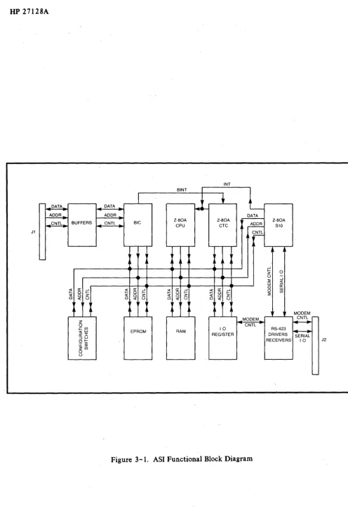
FUNCTIONAL THEORY OF OPERATION
A functional block diagram of the ASI card is shown in figure 3-1. Reference also should be made, as necessary, to the schematic logic diagram contained in figure 7 -1. Note that figure 7 -1 con-sists of three sheets. References to this figure will be as follows: l-A2, 7-1; 2-C6, 7-1, etc.; where the first number, 1 through 3, refers to the sheet number; the combination of letters A through E and numbers 1 through 38 (A2, C6, etc.) refer to the quadrants on the individual sheets; and 7-1
refers to the figure number.
The ASI card contains the following major components:
*
Z-80A CPU (Central Processing Unit)*
Z-80A S10/2 (Serial Input/Output)*
Z-80A CTC (Counter/Timer Circuit)*
BIC (Bus Interface Circuit) plus support circuits*
8K-byte EPROM*
2K - byte static RAMINT BINT
,-- I'
DATA DATA
!-4H- '
-ADDR ADDR DATA
CNTL BUFFERS CNTL BIC Z-80A Z-80A Z-80A
CPU CTC ~ S10
J1 CNTL
I ' r
-If Lr AI'
L-A A
...J
~ 0
z
0
-~ ...J <I: LU a:
a: 0
~ ...J
~ a: ...J
~ a: ...J
~ a: ...J 0 LU
0 ~ 0 ~ 0 ~ 0 ~ (j)
<I: 0 Z <I: 0 Z « 0 Z <I: 0 Z ~
0 « 0 0 <I: 0 0 <I: 0 0 <I: 0
If • It .It It ,
I' AI' ~
,
MODEMZ MODEM
I.CNT~r-0 CNTL
i=fB EPROM RAM 10 RS-423 ~
~I REGISTER DRIVERS
::::lO SERIAL
<.9':: RECEIVERS 10 J2
U:~
Z(j)
0
0
'
[image:28.621.54.550.27.750.2]The heart of the ASI is the Z-80A CPU (2-A26,7-1). The CPU controls the Z-80A S10/2 (3-B34, 7-1), the Z-80A eTC (3-B33, 7-1), the EPROM (2-B24, 7-1), the RAM (2-B22, 7-1), and the BIC gate array (l-A4, 7-1).
The serial asynchronous data and modem control signals are received and transmitted through the RS-423 drivers and receivers. The RS-423 drivers and receivers are controlled by both the SIO and the I/O register (3-E34, 7-1).
A brief description of the function of each block shown in figure 3-1 is as follows:
The BIC is used to bridge the communication between the I/O channel and the Z-80A CPU.
The 8K-byte EPROM is used to store the firmware.
The 2K -byte static RAM is used for I/O buffering and storage of temporary data.
The CTC contains four separate timer/counters, the function of each timer/counter is as follows:
*
The first timer/counter is used to generate transmit and receive baud rates for both SIO channels.*
The second timer/counter is used as a relative timer. Note that the character-relative timer divides the baud rate from a bit-per-second value to a character-per-second value. Although the bits are sent as fast as before, the character-relative timer can cause a time interval to be inserted once a character has been sent. This gives the device more time to handle the data (print it out, for example). The number of start and stop bits are considered during the division.*
The third timer/counter is used by the ASI's firmware for general purpose tasks such as host ENQ/ ACK timer, modem connection timer, no activity disconnection timer, etc.*
The fourth timer/counter is used to detect interrupts from the BIC.The SIO performs parallel-to-serial and serial-to-parallel conversion of the data on the data bus. The SIO also generates some of the modem control signals.
The I/O Register, which can be read from or written to,contains latches and buffers for the special modem control signals.
The internal loop back circuit provides the signal loop back paths for testing the transmit and receive circuits on the ASI card (with the exception of the receivers and drivers).
MEMORY ADDRESS SPACE
An 8K-byte EPROM (see 2-B24, 7-1) and a 2K-byte RAM (see 2-822,7-1) are used for memory. The memory address space is allocated as shown in table 3-1.
1/0
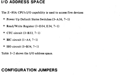
ADDRESS SPACE
The Z- 80A CPU's I/O capability is used to access five devices:
*
Power Up Default States Switches (3-A36, 7-1)*
Read/Write Register (3-034, E34, 7-1)*
CTC circuit (3-B33, 7-1)*
BIC circuit (1-A4, 7-1)*
SIO circuit (3-B34, 7-1)Table 3-2 shows the I/O address space.
CONFIGURA TION JUMPERS
An 8-position programmed jumper is included on the ASI card. The definitions of the jumper are shown in table 3-3. The jumpers are set at the factory and should not require any additional modif ica tion.
INTERFACING TO BIC
Interface between the I/O channel and the ASI card is handled by the BIC gate array (see l-A4, 7-1). Briefly, the BIC provides a standard method of interfacing to the I/O channel bus. I/O ad-dresses between the BIC and the I/O channel are shown in table 3-2.
The BIC configures the direction of the data path between the backplane and the Z.-80A CPU, and provides the necessary handshake signals for interfacing to the backplane.
[image:30.613.67.553.177.443.2]Table 3 -I Memory Address Map
BIT ASSIGtK:NTS
FUNCTION
A15
A14
A13 - AO
MEMORY
ADDRESS
HEX
--64K ---- --- --- -
---Not u5ed
--32K
---Thi!5 area i5
for RAM
expan!5ion
FFFF H
--- --- --- --8000
H---Becau5e the RAM i5
7FFF
H
alwaY5 5elected in thi5
part of memory,
multiple image5 of the
RAM exi5t
--18K --- --- --- ---
--4800H---RAM
X
1
47FF
H
--16K --- --- --- ---
--4000H---Pre5ently
3FFF
Hnot u!!sed.
Thi5
loca-tion can
be
u5ed to
addre!55 the
additional
8K
bytesof
EPROM.
X
o
-- 8K --- --- --- ---
--2000H---EPROM
X
0
X
1FFF H
H---Table 3-2. I/O Address Space
liD
BIT ASSIGNMENTS
ADDRESS
FUNCTION
A7
AS
AS
A4
A3
A2
A1
AO
HEX
Power Up
Switch
1
1
1
1
X
X
X
0FO
R/W
Register
1
1
1
1
X
X
X
1
F1
CTC
Channel
01
1 01
X
X
0 0DO
CTC
Channel
1 1 10
1X
X
01
D1
CTC
Channel
2 1 1 01
X
X
1
0D2
CTC
Channel 3
1
1 01
X
X
1
1D3
BIC
Register 0
1
01
1
X
0 00
BO
BIC
Register' 1
1 0 11
X
0 01
B1
BIC
Register 2
1 0 1 1X
0 1 0B2
BIC
Register 3
1
01
1X
01
1B3
BIC
Register 4
1 0 11
X
1 0 0B4
BIC
Register 5
1 0 11
X
1 0 1B5
BIC
Register S
1 0 1 1X
1
1 0 BSBIC
Table 3-2. I/O Address Space (Continued)
1/0
BIT ASS I GMMENTS
ADDRESS
FUNCTION
A7
AS
AS
A4
A3
A2
A1
AO
HEX
SIO Chan. A
Data
0
1
1
1
X
X
0
0
70
SID Chan. A
Control 0
1
1
1
X
X
0
1
71
SID Chan. B
Data
0
1
1
1X
X
10
72
SID Chan.
BControl 0
1
11
X
X
-1 173
X
=
Don't care
Table 3-3. Jumper Definitions
JUMPER
FUNCTION (IF CONNECTED)
PURPOSE
1
WE to pin 23 of RAM socket
Configuration for 2K-8K
2
A11 to pin 23 of RAM socket Used with Jumper 1
3
Enable wait state generator Allows 450 n5ec EPROM
4
Enable m1 from Z80
Manufacturing Test
5
Not used
Table 3-4. Connections Between BIC And Z-80A CPU
DIRECTION
OF SIGNAL
SIGNAL LINES
WITH RESPECT
IN BIC
TERMItiATION
TO BIC
FUNCTIOti
SEL-
Output of
in
Enable one of the 8
the addre!!!!
BIC regi!!ter!!
Decoder for
(addre!!!!ed
by·lower
the BIC
3 bit!! of addre!!!!
bu!!)
I tiT-
CLK/TRG3 of
out
Interrupt Z-80A
CTC
CPU. INT-
m!l!!kable
by !!oftware
RESET-
RESET- of
out
Re!!et!! card when an
Z.;...BOA CPU,
IFC or DCL i!!
CTC and SIO
a!!5erted, or PPON
i!! de-a55erted
0[7:0]
07-DO of
in/out
Bidirectional
tri-Z-BOA CPU
!!tate data bu!! line!!
DS[O]
WE- of Z-BOA
in
Write enable. Dsta
CPU
will be written into
one of the BIC
regi!!ter!!
05[1]
RD- of Z-80A
in
Read enable. Dste
CPU
will be read from one
of the BIC regi5ter!!
A[2:0]
A2-AO of
in
Addre!!!! line!! for
Z-80A CPU
addres!iing BIC reg!!.
A5-
Ground
in
Not u!ied
XENO-
+5 through
in/out
Not u!!ed
10K re5i!itor
DTR-
+5 through
in
Not u!!led
10K resi!!tor
RDY-
Floating
out
Not used
INTERFACING TO
RS-232-C/RS-423
DEVICES
Asynchronous serial data and modem control signals are transmitted and received through the SIO (3-B34, 7-1) and the I/O Register (3-034, E34, 7-1), (a read/write port).
A summary of RS-232C/RS-423 signals which are supported by the ASI is presented in Section 2, table 2-4.
Z-80A SUBSYSTEM
The Z-80A CPU, SIO, and eTC control the operation of the ASI. The following paragraphs describe the operation of these components and related circuitry:
'" CPU (Central Processor Unit)
'" System Clocks
'" SIO (Serial Input/Output)
'" CTC (Counter/Timer Circuit)
'" Priority Interrupt Structure
'" EPROM
'" Power-Up Default States Switches
'" I/O Register
'" Reset Circuit
'" Wait State Generating Circuits
CPU (Central Proce$sor Unit)
com-The Z-80A CPU employs a register-based architecture which includes two sets of six general-purpose registers which can be used as individual 8-bit registers or 16-bit register pairs. Additional 8-bit registers include two sets of accumulator and flag registers, and the interrupt vector and memory refresh registers. Additional 16-bit registers include the stack pointer, program counter, and two index registers.
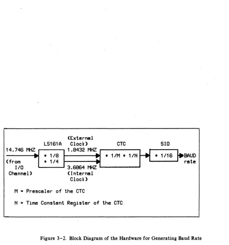
System Clocks
A 7 4LS 161 A counter (see 2 - D 2 2, 7 -1) is used to derive two system clocks from the 14.7456 MHZ I/O channel clock signal CCLK. The names and functions of the clocks are as follows:
PHISYS, which has a frequency of 3.6864 MHZ, is used for driving the Z-80A CPU, SIO and CTC circuits.
PHICTC, which has a frequency of 1.8432 MHZ, is used as an external clock for the CTC to genera te the baud rates.
SIO (Serial Input/Output)
The I/O addresses of the SIO (3-B34, 7-1) are shown in table 3-2. There are two independent full-duplex channels on the SIO, channel A and Channel B. Channel B is the primary channel, and Channel A is a secondary channel. The SIO also generates some of the modem control signals, as shown below:
INPUT MODEM CONTROL SIGNALS:
CTSB, CTSA
USed as CS (Clear To Send) for the primary and secondary channels, respectively.
DCDB, DCDA
Used as RR (Carrier Detect) for the primary and secondary channels, respectively.
SYNCA
OUTPUT MODEM CONTROL SIGNALS:
RTSB, RTSA
Used as RS (Request To Send) for the primary and secondary channels, respectively.
DTRB
Used as TR (Data Terminal ready) for the primary channel.
CTC (Counter ITlmer Circuit)
The CTC (3-B33, 7-1) is an I/O addressable port from the Z-80A CPU perspective; its addresses are defined in table 3-2. The CTC circuit has four independent counter/timers. The functions of the counter /timers are:
Channel 0 is used as programmable baud rate generator for both channel A and channel B of the SIO chip.
Channell is used as programmable baud rate generator for character-relative timing (i.e., the GAP timer). Note that character-relative timing divides the baud rate from a bit-per-second value to a character-per-bit-per-second value. The number of start and stop bits are con-sidered during the division.
Channel 2 is reserved for the use· of firmware for general purposes tasks such as host ENQ/ ACK timer, modem connection timer, and no activity disconnection timer, etc.
Channel 3 is used to detect BIC interrupts. Basically, the CTC interrupts when the BINT- output of the BIC goes low, and no higher priority I/O device is interrupting.
(External
LS161A
Clock)
::~:~ ~Z~
:~~:
11.8432~~
lID -. - - - 3.6864 MHZ .
Channel)
(Internal
Clock)
M • Prescaler of the CTC
CTC
SID
• 11M • 11N
r' ·
1/16I-~~~
H • Time Constant Register of the CTC
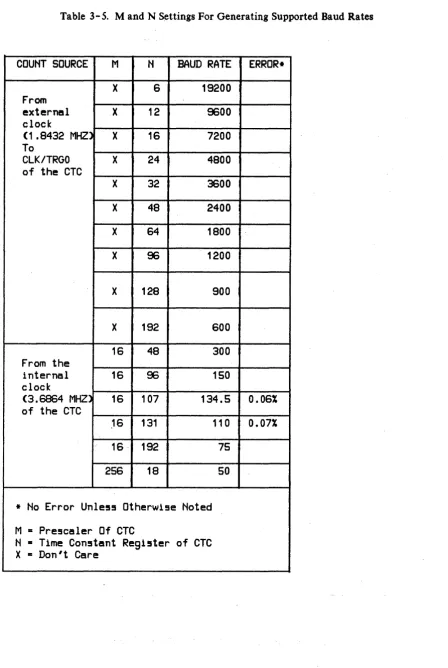
[image:38.613.62.527.61.556.2]Table 3-5. M and N Settings For Generating Supported Baud Rates
COUNT SOURCE
MN
BAUD RATE
ERROR*
X
6
19200
From
external
X
12
9600
clock
(1.8432
MHZ)
X
16
7200
To
CLK/TRGO
X
24
4800
of the CTC
X
32
3600
X
48
2400
X
64
1800
X
96
1200
X
128
900
X
192600
16
48
300
From the
internal
16
96
150
clock
(3.6864
MHZ)
16
107
134.5
0.06%
of the eTe
,16
131
110
0.07%
16 . 192
75
256
18
50
* No Error Unle5s Otherwise Noted
M
=
Pre!5caler Of eTe
[image:39.615.100.549.74.743.2]BINT FROM BIC
FROM SIO , -_ _ --, CTC lEI INT
1 - - - 1 ZC/T03
lEO
TOZ-80ACPU
Figure 3-3. DIC Interrupt Detecting Circuits
BINT
lEO
ZOT03 INT
~"80A
CPU
INTERRUPT REQUEST FROM BIC
•
INTERRUPT SERVICE
FROM~-80A
CPU
•
,L-___
~ S~---l ~-80A CPU EXECUTES• RNT1 INSTRUCTION
4---1..; S ' T - - - l1
~--~~s---2'6lSYS
[image:40.613.93.498.61.677.2]Priority Interrupt Structure
The Z-80A CPU is programmed in Mode 2 for vector interrupt. The maskable INT- (Interrupt) pin of the Z-80A CPU is driven by the open drain gates from the INT- (interrupt) pins of the SIO and CTC. The SIO and CTC are configured in a daisy-chain structure, where the SIO has higher priority.
The priority interrupt structure of the Z-80A Subsystem is:
Highest Priority
Lowest Priority
EPROM
SIO Channel A Receive SIO Channel A Transmit SIO Channel A External/Status SIO Channel 8 Receive
SIO Channel 8 Transmit SIO ChannelB External/Status CTC Channel 0
CTC Channel 1 CTC Channel 2 CTC Channel 3 (BIC)
The memory address of the EPROM (2-824, 7-1) is shown in table 3-1. The standard EPROM has an access time of 250 nsec. The ASI can fetch instructions from this EPROM without any wait states. If the wait state generator is enabled (see jumper configuration), EPROMs as slow as 450 nS can be used.
Power Up Default State Switches
Eight switches (see 3-A36, 7-1) are provided for configuring the default state/mode of the card during power up. Definitions of. the functions of the switches are shown in Section 2, table 2-1.
I/O Register
[image:41.620.87.523.190.397.2]Table 3-6. Definitions Of The Bits of the I/O Register
BIT ASSIGNMENTS
OPER-
D7
00D5
D4
D3
D2
D1
ATION
Read
Not used
IC
note 2
Write
SR
Fiber LED
Self-Test
not used
note 6 note 1 note 4 note 5
Note 1: Set this bit to !!elect TTL level read data for
fiber optic!!.
DO
JlY1
note3
Note 2:
IC (Incoming Call), which i!! B19 at the card edge
Note 3: OM (Data Mode), A11,B11, A12 at the card edge
Note 4: LED Driver bit. The LED is ON when this bit 1s low
Note 5: When Self-Test bit is cleared, the transmitting
lines will loop back to the receiving lines and the
data outputs will be di!!abled. Bit DB mu!!t be zero
for data to loop back properly.
[image:42.617.57.505.63.740.2]Reset Circuit
The output of the Reset circuit (see 2-D23, 7-1) drives the RESET pins of the Z-80A CPU, SIO, and CTC; and the CLEAR pins of the I/O Register. The Reset circuit is activated by the RESET- pin of the BIC. When the Reset circuit is activated, its output will be pulled low for more than 3 clock
cycles of PHISYS. .
Figures 3-5 and 3-6 show the Reset circuit ·and the timing diagram, respectively.
TRUTH TABLE FOR lS74A
PR ClR D Q Q
(FROM BACKPLANE) 0 0 x 1 } TEMPORARY.
PPON ClR 0 1 x 1 0
0 x 0 1
RESET 1 1 0 } RISING EDGE TRIGGER.
(FROM BIC) 1 0 0
+5 QSYS
10K QCTC
BACKPLANE CClK RIPPLE 1 - - - . . 1
CLOCK L - - _ - - - I ClK
14.7456 MHZ
2 3 4 5 6 7 8 9 10 11 12 1314 15 CCLK
CLR
...--_ _ _ _ _ 33/4 ~SYS CYCLES _ _ _ _ _ _ .... ,. _ _ _ _ _ _ _
RESET
~L
_________________________________________~
Figure 3-6. Reset Circuit Timing Diagram
Wait State Generating Circuit
The standard EPROM has a 250 nsec access time and does not require the use of the Wait State Generating circuit. Wait states are provided to allow use of slow EPROMs. The maximum memory access time that can be used is 450 nsec, which is longer than the memory access cycle of the Z-80A CPU. The Wait State Generating circuit, and its timing diagram are shown in figures 3-7 and
[image:44.613.43.551.69.556.2]SHORT JUMPER TO ENABLE WAIT STATE CIRCUIT
'QSYS - - - - I >
+5
+5
Q
LS74A
[image:45.620.68.562.50.679.2]~----WAIT
Figure 3-7. Wait State Generating Circuit
'QSYS T1
EPROMCE
EPROMCE
T2 TW T3
PROGRAMMING
I~
Many of the ASI's firmware features are programmable by the user. Firmware features include provisions for meeting
u.s.
and European modem ;-equirements. The firmware also provides complete flexibility for software handshake to most terminals, and for terminal emulation. In ad-dition, options such as baud rate, break detection and generation, etc., are programmable.A Z-80A microprocessor Central Processing Unit (CPU), a Z-80A Serial Input/Output (510), and a Z - 80A Counter/Timer Circuit (CTC) allow the ASI to achieve functional flexibility. This allows modem control as well as direct interface to a wide variety of devices.
The ASI contains firmware implemented capabilities that simplify interfacing tasks for the host computer. This allows the host computer to provide more time and space for users. These firm ware functions can be disabled to allow the host computer to directly control most operations so that spe-cial needs can be met.
ASI PROGRAMMABLE FEA TURES
Features and options of the ASI which can be controlled programmatically are as follows:
• Types of Protocol (EIA RS-232-C and RS-423, and CCITT V.24 and V.28)
• Number of Stop Bits (1, 1.5, or 2)
• Transmission Mode (asynchronous only in simplex, full-duplex, or echoplex)
• Parity (none, odd, even, 0, orl)
• Baud Rate (50, 75, 110, 134.5, 150, 300, 600, 900, 1200, 1800, 2400, 3600, 4800, 7200, 9600, or 19200)
• Break Detection and Generation
• Edit Mode Option to Process Backspace and Line Deletion
• Single Text Terminator Character(s) • Double Text Terminator Character • Prompt Sequence Detection
• Host controlled ENQ/ ACK Handshake to Device with Programmable Time-Out • Device controlled ENQ/ ACK Handshake
• Host controlled X -ON/X -OFF Handshake • Device controlled X -ON/X -OFF Handshake • Type -ahead Mode
• Alert 1 Mode
• Automatic Output Separator(s) for Transmitted Text • Single Text Terminator (echo a CR-LF in echoplex mode)
PERFORMANCE
The ASI will allow communications with a terminal at 19200 baud in full-duplex mode with all the above features enabled. This mode relies on the TYPICAL HUMAN INTERACTION speed to perform some of the special character processing. If the receive data is coming in continuously with no pause between each character (as in large screen, block-mode transfer), THE CARD CAN ACCEPT THE DA T A AT THA T SPEED IF ALL THE CAPABILITIES, LIKE EDIT MODE, SOFTWARE HANDSHAKE,2-CHARACTER SEQUENCE SEARCH, ETC., ARE DISABLED. HOWEVER, ONE TEXT TERMINATING CONDITION SUCH AS SINGLE TEXT TERMINATION WITH ONE TERMINATING CHARACTER SPECIFIED, MAY BE ENABLED TO TERMINATE THE
INCO~lING TEXT.
TRANSACTIONS
Each transfer between the ASI and the host computer is called a "transaction", and occurs over the I/O channel. Each transaction represents a single read or write (data, status, etc.)
Connect Logical Channel (CLC) Request Format
The Connect Logical Channel (CLC) request block has the following format:
-:-I-~-I-:-I-~-I-~-I-~-I-~-I-~-byte 0 high byte logical channel no.
1 low byte logical channel no.
2
-~-I~~;I;~~!;:~I-~~!:~~:-~~~~--- -~-I~~;I;~~!;:~I-~~!:~~:-~~~~--- -~-I~~;I;~~!;:~I-~~!:~~:-~~~~---1-~-I~~;I;~~!;:~I-~~!:~~:-~~~~--- -~-I~~;I;~~!;:~I-~~!:~~:-~~~~---1-~-I~~;I;~~!;:~I-~~!:~~:-~~~~---1-~-I~~;I;~~!;:~I-~~!:~~:-~~~~---1-~-I~~;I;~~!;:~I-~~!:~~:-~~~~---
---1---1---1---3 5ubfunction code
---1---1---1---1---1---1---1---4 port ID
---I---I---I---I-~-I---I---I---5 data length high byte (16-blt
. un!!!ligned
6 data length low byte integer)
---~--E~D
where
logical channel n um ber
Assigned by the host for each transaction. The card firmware will keep the ID with each transac-tion until it is completed.
S bit
Used by all nonblock read device data requests and by the last block of the block read device data request. If the S bit is set, any remaining data in the current read record will be available for the next read request. If the S·bit is clear, any data remaining in the current record will be discarded after the read is completed.
BLK
0= non-block data transfer
req uest code
O· not used
1 • read device data
2 • write device data
3 • control device
4 • read card inf orma tion
5 • write card configuration data
6 • control card
7 • read trace data (not available on the ASI card)
8 - 1 5 • reserved
subfunction code
The content of this field is dependent on the type of the request.
port ID
The ASI supports only one port; therefore, this value will always be zero.
data length
Required for all read or write requests. All other requests should contain zeros.
CAPABILITIES
Receive Character Processing
Each received character is processed in the following order:
1. a. If any error condition occurred, the current receive record is terminated. The record is then made available for the host. The error condition includes data overrun, parity, and framing. If the firmware is controlling a modem, the loss of the DM signal or the loss of the RR signal will also terminate the record.
b. If the Signal Character Detection option is enabled, check for signal character match. See the paragraph "Additional Options" (see table of contents for page number) for details.
2. If any of the four software handshake options is enabled, check the character as follows:
a. For the Host ENQ/ ACK Handshake option, check the character for an ACK.
b. For the Device ENQ/ ACK Handshake option, check the character for an ENQ.
c. For the Device X-ON/X-OFF Handshake option, check the character for either X-ON or X-OFF.
d. For the Host X "';ON/X -OFF Handshake option, send an X -OFF if there is not enough space remaihing in the receive buffer.
3. If the Edit Mode option is enabled, check the character for backspacing and line deletion. If the Quoting Mode option is enabled, and an edit character is encountered, and the previously received character is a quote character, replace the quote character with the edit character.
4. If the Character Stripping option is enabled, check for the null, the "DEL",or the "FF" characters.
5. a. If the Single Text Termination option is enabled, check the character to see if it isa single text terminator. If yes, terminate the current receive record and make it available to the host. If the Strip The Single Text Terminator option is disabled, add the single text ter-minator to the buffer.
b. If the Quoting Mode option is enabled and the previously received character is a quote character, replace the quote character with the single text terminator. The record is not ter-mina ted in this case.
7. If the Prompt Sequence Detection option is enabled, check the incoming characters for a prompt sequence. If a prompt sequence is found, terminate the current receive record and make it available to the host.
If the received character does not match any of the conditions described in conditions 1 through 7, the character is now added to the current record.
8. a. If the End-On-Count option is enabled, a check against the end-on-count is made. If the count is exhausted, the current record is terminated with the "end -on -count" termination.
b. If the read request length is enabled, decrement the counter. If the count reaches zero, terminate the record with the "text terminated by the card, no more data" code.
c. If the current count matches the internal buffer count limit, terminate the record with the "text terminated by the card, more data coming" code.
9. If the Alert 1 option is enabled, the card will notify the host that at least one character was received. See the paragraph "Alert 1 Read Mode" (see table of contents for page number) for a further discussion of the Alert 1 option.
As mentioned earlier, the order of processing the received character as described in steps 1 through 9 is the precedence implemented by the ASI firmware. Only one type of termination is as-signed to each receive record.
The preceding descriptions frequently use the term "current receive record". The "current receive record" is the currently active record that can receive data from the device. If the current receive record does not exist, a record is created and the character, or the termination condition, is added to the record.
Note that some conditions, such as single text termination, double text termination, or prompt se-quence detection may cause a generation of a record which contains no data. You should be aware that the text record may be of zero length. In this case, you will be notified of the condition that caused the termination in the request status block.
Receive Error Conditions
The firmware wIll normally terminate the current receive record when any error condition is sensed. If the Do Not Terminate On Error option is set, the firmware will not terminate the record. Instead, a user specified replacement character will replace the bad incoming character, see the IIError HandlIng" paragraph (see table of contents for page number) for further details.
For data overrun, parity, and framing error, the character causing the error will be added to the current receive buffer. For the lost of DM or RR modem signal, any data remaining in the SIO receive buffer will be read and added to the current receive buffer.
Software Handshake with the Device
Four software handshakes are available between the host and the device:
1. Host controlled ENQ/ ACK handshake
2. Device controlled ENQ/ ACK handshake
3. Host controlled X -ON/X -OFF handshake
4. Device controlled X -ON/X -OFF handshake
IndIvidual software handshakes are enabled by using the WCC, SF 9 (Write Card Configuration, Subfunction 9). The handshake processing firmware is enabled by using WCC, SF 1. The characters defined for the ENQ, ACK, X -ON, and X -OFF characters are programmable by using the \VCC, SF 22, 23, 24, and 26. The following discussion will assume the default characters defined as follows.
handshake character
ENQ ACK
X-ON
X-OFF
default ASCII character
ENQ ACK
DC1
DC3
hex value
05
HOST CONTROLLED ENQ/ ACK HANDSHAKE. This option is used to pace the data transfer from the card to the device to prevent the device from losing any data due to its slow internal processing speed.
The firmware sends an ENQ character after the pacing counter has counted down to z.ero. The card then waits for an ACK character before proceeding to transmit more characters from the transmit buffer. This will ensure that buffer space in the device is available.
You can program the pacing counter by using the Write Card Configuration, Subfunction 25 (WCC, SF 2 5). Th~ default count is 80 bytes. The counter is decremented after each character is transmitted.
There is a programmable host ENQI ACK timer to prevent the firmware from being hung if the
ACK is lost or if the device is off-line and then comes on-line. The card will transmit an ENQ again until an ACK is received. You have the option of disabling the ENQ retry after the time-out by setting the tlsend message after ENQ timer time outtl bit in the Write Card Configuration, Subfunction 9 (WCC, SF 9). In this case the card will proceed with the data transmission from where it stopped.
The host ENQ/ ACK timer is programmed by using the WCC, SF 18. The default value used is 5 seconds.
To prevent any deadlock problems this handshak~ should not be enabled if the device X -ON/X -OFF handshake is enabled.
DEVICE CONTROLLED ENQ/ ACK HANDSHAKE. For the ENQ/ ACK handshake from the device, the card will send an ACK for every ENQ received if there is enough space available to hold 80 characters.
To prevent any deadlock problems, this handshake should not be enabled if the host X-ON/X-OFF handshake is enabled.
HOST CONTROLLED X -ON/X -OFF HANDSHAKE. This handshake protocol allows the card to pace the data transfer from the device to the card. The card will send the X-OFF character (DC 3 or CTRL-S) to the device to stop data transmission when there is not enough space in the receive buffer (the user has at least ten character times to stop transmission). The card will send the X -ON character (DC 1 or CTRL-Q) when buffer space becomes available again.
DEVICE CO~TROLLED X-ON/X-OFF HANDSHAKE. This handshake protocol allows the device to pace the data transfer from the card to the device. The device will signal the card to stop transmit-ting da ta by sending an X -OFF character. The receiving device restarts data transmission by sending the X -ON character, or by sending any characters if the Implicit Device X -ON option is enabled with WCC, SF 31.
The ASI firmware will stop data transmission as soon as the X-OFF character IS received; however)
up to two characters may be transmitted before the stoppage.
To prevent any deadlock situation, this handshake should not be enabled if the host ENQ/ ACK handshake is ena bled.
Edit Mode
The Edit Mode option is enabled by setting the Edit Mode bit in the data block of the WCC, SF 1. The Edit Mode option is disabled by clearing the Edit Mode bit.
\\'hen working at a terminal connected to this card, 2 types of editing capabilities are available. The first is backspace, which deletes the previously typed character; and the second deletes the current line. In addition, a Quoting Mode option allows the insertion of the edit character into the text buffer without performing any editing.
BACKSPACE. The firmware uses the character BS (hex 08) to indicate a backspace function. This character is generated by pressing the BACK SPACE key or by typing CNTL-H. In addition, you can programmatically change the backspace character to any desired character by using the wee, SF 6. Three options are available to indicate that a backspace has occurred when the card is in echoplex mode. The first option is "backspace echo". This option echoes a backslash character) fol-lowed by the character that was deleted from the input buffer. The second option is "backspace overwrite". This option is very useful for CRT-type terminals. The firmware backspaces a character, writes a space character, and then backspaces again.
The third option is "backspace onlY". This option echoes only the backspace character to move the cursor under the deleted character.
The Backspace option is programmable by using WCC, SF 8.
LINE DELETION. The firmware uses the character DEL (hex 7F) as the line deletion charac-(ter. As with the backspace character, you can program the line deletion character by using the
WCC, SF 7.
The line deletion character causes the card to delete the current line, if any. If the card is in echoplex mode, it will write one backslash, then do a carriage-return/linefeed.
Character Stripping
You have the option of stripping certain characters from the input stream. This includes stripping null's, DEL's, and FF's (base 16). Any character stripping, except for text terminator character stripping, must be enabled by setting the Character Stripping option in the data block of the WCC, SF 1. If the Character Stripping option is enabled, you specify which character to strip with the WCC, SF 8.
Note that the "DEL" character is also used in edit mode to delete a line. If the Edit Mode option is enabled and "DEL" is the line deletion character, the "DEL" character will be processed as a line deletion character.
You also have the option of not stripping any text terminators by using the WCC, SF 8. Normally, all text terminato